LCD Driver Has Own Voltage Boost Converter After All

I took apart an AT&T CL84209 cordless phone system and kept one of the handset’s circuit boards attached to its LCD unit. This allowed me to power up the circuit board and probe how its main processor controlled what’s shown on the LCD. I then took the LCD off of its board to take a closer look at the related circuitry.

Probing data indicated there was +5.2V on one of the LCD pins, and I had guessed it was supplied by a voltage boost converter somewhere else on the circuit board. I learned what they usually look like from the time I dug into the circuit board for a laptop screen, which included a boost converter to power its white LED backlight. On this handset circuit board, I see at least one assembly of an inductor next to a diode close to a capacitor, all the elements I now associated with a boost coverter.

But when I traced the phone handset circuit board, I didn’t find a +5.2V line going to the LCD. I found only a pair of capacitors. One of which connected the two square-wave generating pins (7 and 8) and another capacitor connected the +5.2V line to the +3.3V line. (Pins 5 and 6.) I don’t recognize what this arrangement does, but I could replicate it on my breadboard and see what happens.

The analog capture showed what happened: We now see pin 6 sit at 3.3V immediately upon initial power-up and rise up to +5.4V in response to the first I2C configuration message. Finally matching the pattern I saw on the original capture. This is amazing! The LCD driver chip only needs a +3.3V power supply and from that it generates its own +5.4V. There must be a built-in voltage boost converter with inductor and diode (or their functional equivalents) internal to work alongside an external capacitor. I thought I had learned enough about boost converters to recognize them when I see them, now I know I’m wrong. Earlier I had put a capacitor between the boost converter output line and ground, and that didn’t do what it did when I put the capacitor between boost output and +3.3V. I clearly have more to learn more about boost converters. But at least now I’m finally driving this LCD properly.

Unsoldering CL84209 Handset LCD

After mapping out the segments on the LCD salvaged from the base station of an AT&T CL84209 cordless phone system, I have reached the limits of what I can do in the absence of additional information. It has been wonderfully instructive to have a handset from the same system with its own LCD. I found that both LCD respond to the same command protocol, so I could power up the handset circuit and watch what happens under a logic analyzer then try to replicate the same behavior for the base station LCD. Now it is time for me to remove the LCD from the handset circuit board. I wanted to do so for two reasons:

  1. I don’t really want to keep the entire handset circuit board. It is designed to talk to a base station that no longer exists.
  2. It might be hiding some useful secrets underneath the LCD. I have a working knowledge of how all the pins work, but I might learn more from probing the circuit board independent of the LCD.

A bit of time with the solder station and I have separated the LCD to see that there’s… almost no components hidden underneath.

Just a single side-illumination LED in the upper right corner marked LED3. It feeds into a backlight mechanism much less sophisticated than a Fire tablet’s backlight.

But now we can see copper traces on this side of the circuit board. I was happy to see that my arbitrary left-to-right pin numbering matched what’s silkscreened here, purely by accident! I had thought pin 1 or 5 could be the power supply, and decided 1 was enable and 5 was supply. Now I get confirmation because 1 is a very narrow signal trace and 5 is a much thicker power trace. 2 and 3 were also thin digital signal lines for I2C, and 4 is connected to a big grid-patterned plane consistent with ground.

Those were great confirmations of my earlier guesses, but even better is information about the rest of the pins. The surprise was that pin 9 appears to be connected, because I had thought it was one of the capacitors I saw on the back side. Another surprise is that pin 6, which I thought would connect to a +5.2V supply, seems to connect only to one of four vias (marked by white circles) going to the other side of the circuit board.

Following those four vias to the other side, I find a pair of capacitors. Now that the LCD has been unsoldered, my multimeter could measure their capacitance: the one on the left read 823nF and the one on the right 775nF. Looking over popular capacitors on Digi-Key, these might be 0.82uF +/- 10% capacitors. But even more importantly: now that I can see the traces, I understand one capacitor bridges the +3.3V line and the +5.2V line, and the other bridges the two square wave lines. My electronics knowledge isn’t good enough to know what this means. But once I replicated this part of the circuit, I saw a voltage boost converter in action.

Quadrature Encoder Rotary Knob with Detent

In order to create a segment map for a salvaged LCD unit, I soldered a rotary knob into my Arduino circuit so I could interactively select which segment to activate. It came from this particular Amazon multipack listing (*) which was the lowest bidder that day. This knob reports rotary motion via quadrature encoding, and it has a mechanical detent for tactile position feedback. (Twenty detents per revolution of the knob, or 360/20 = 18 degrees per detent.) It also responds to push like a button. The segment map project was my first unit from the multipack, and it seems to function properly. Even better, it doesn’t “feel cheap” in its tactile sensation, so I’m happy with this particular multipack. And because it was so inexpensive, I decided to take one apart and look inside.

The entire assembly is held together by folded sheet metal. Bending its four fingers aside allowed me to separate the device into individual subcomponents. The pushbutton mechanism is at the bottom, a very simple construction where the two pins connected to two sheets of slightly separated metal. There’s a slight convex curve to the metal acting as spring. Pushing on the knob pushes these two sheets together. Overcoming the convex curvature gives us the tactile “click” of the button press and gives us electrical conductivity between those two sheets. Usage: tie one of these two pins to ground and connect the other pin to the microcontroller input pin with either internal pull-up or external pull-up resistor so it normally reads high. When knob is pressed, the pin will be shorted to ground so it reads low.

The next layer up is the quadrature encoder to report rotary motion. There are two sets of thin metal fingers that stay in a fixed position, making contact with alternatively conductive/non-conductive portions of a wheel that turns with the knob. Here is an illustration of the electrical conductivity between these fingers and their interface pins:

The center of these three pins connect to both sides. Each of the other two connect to their side of the wheel. Usage: connect the center pin to ground. Connect the other two pins as quadrature A and B signals to microcontroller with internal pull-up or external pull-up resistors.

Above the wheel is the detent mechanism. For this particular device, there is a detent every four quadrature transitions. When it is stopped at a detent neither of the two side pins are connected to ground. (high/high) When turning from one detent to the next, it will quickly cycle through the other three states (high/low + low/low + low/high. Or the reverse order low/high + low/low + high/low if spin the opposite direction) before stopping at high/high again on the next detent.

These quick transitions meant polling would not be fast enough to read this encoder. We require hardware interrupt support to ensure we don’t miss steps. As I did for the Toyota faceplate investigation, I used Paul Stoffregen’s Encoder Arduino library. This time running on ESP8266 Arduino Core instead of ATmega328, it reliably read knob transitions using ESP8266 interrupts.

(Note: at the time of this writing, the latest public release is v1.4.2 which has problems running on an ESP8266. I had to clone the repository directly to pick up at least this fix among others.)


(*) Disclosure: As an Amazon Associate I earn from qualifying purchases

CL84209 Base Station LCD Segment Map

I have generated a printable lookup chart for the character set of an unknown LCD controller. This chip is embedded inside a black blob along the top edge of an LCD I salvaged from the base station of an AT&T CL84209 cordless phone system. The character set dictates what is rendered in two lines of 15-character alphanumeric text, each character is a dot matrix 5 pixels wide and 7 pixels tall. Below these two lines is a set of custom segmented LCD that can be controlled with 16 bytes, but there appear to be far fewer than 16*8 = 128 segments to control. A segment map will tell us which segments correspond to which bits.

I don’t have the datasheet for this chip, so I don’t know how it numbered its segments. I decided to mostly follow the precedence set by Sanyo LC75853 by numbering both bits and bytes in least-significant-first order. The difference for this map is that while LC75853 started counting from one, I’m going to start counting from zero.

My first attempt at mapping out these segments toggled them on/off alongside the character set data. When displaying characters starting with 0x00, I turned on all the segments whose number has zeroth bit set. For the character set starting with 0x10, I turned on all the segments with the next bit set, etc. In theory I could look at the on/off pattern as it cycled through 0x00 to 0x70 and determine its binary number. I also printed out the bit pattern to Arduino serial console, which looks like this:

0 1 10101010 10101010 10101010 10101010 10101010 10101010 10101010 10101010 10101010 10101010 10101010 10101010 10101010 10101010 10101010 10101010 
1 10 11001100 11001100 11001100 11001100 11001100 11001100 11001100 11001100 11001100 11001100 11001100 11001100 11001100 11001100 11001100 11001100 
2 100 11110000 11110000 11110000 11110000 11110000 11110000 11110000 11110000 11110000 11110000 11110000 11110000 11110000 11110000 11110000 11110000 
3 1000 0 11111111 0 11111111 0 11111111 0 11111111 0 11111111 0 11111111 0 11111111 0 11111111 
4 10000 0 0 11111111 11111111 0 0 11111111 11111111 0 0 11111111 11111111 0 0 11111111 11111111 
5 100000 0 0 0 0 11111111 11111111 11111111 11111111 0 0 0 0 11111111 11111111 11111111 11111111 
6 1000000 0 0 0 0 0 0 0 0 11111111 11111111 11111111 11111111 11111111 11111111 11111111 11111111 
7 10000000 0 0 0 0 0 0 0 0 0 0 0 0 0 0 0 0 

In theory this can work, in practice I quickly got tired flipping through images and decoding binary numbers by hand. That was a lot more work than having a quadrature encoder knob to interactively select segments to activate. I had avoided wiring in extra components out of laziness, but between manual binary decoding and soldering, I decided a bit of soldering was the easier path towards this segment map:

This map clearly showed this particular segment allocation used less than 5/8 of available segments. Starting from position zero, we would have five bits for five segments (0, 1, 2, 3, 4) then three bits that were unused. (5, 6, 7) Then five more segments (8, 9, 10, 11, 12) and three unused bits (13, 14, 15). This repeats until the final set of five (120, 121, 122, 123, 124) which were also unused.

I was surprised that segment 9 (“MSG#” title for message count) was a separate segment from 4, the rectangular border around message count. I had expected them to be a single segment.

I was also surprised and annoyed at segment 27, which lights up all three horizontal lines of the hour tens digit for the clock plus the lower left vertical segment. For a clock it made sense to restrict the tens digit to 1 or 2. But if so, why did they bother with segment 26 which isn’t useful for either of those digits? I had hoped maybe I could use it as a generic numeral display and not a clock, by leaving 65 and 66 (AM/PM) inactive. But segment 27 means I could only display 1, 2, 6, and 8. I have not yet thought of an interesting non-clock usage under those restrictions.

Obtaining a full segment map marks the end of investigating this base station LCD, I will now try to do the same for the handset LCD starting with its disassembly.


Source code for this investigation is publicly available on GitHub.

CL84209 Base Station LCD Character Set

After a look at the similarities and differences between two LCDs salvaged from an AT&T CL84209 cordless phone set, I was ready to start controlling one myself to get more data. Earlier probing indicated that I2C communication on the handset was 3.3V, so I’m going to use an ESP8266 because it is also a 3.3V part. The Arduino platform should be a good (enough) starting point, using its Wire library to recreate the I2C control messages I saw sent to the handset LCD.

After a quick test program to verify things worked as expected, I wanted to dump out the character set built inside this LCD controller. Since the character data is sent one byte per character, there are potentially 256 different characters in the font. Dealing with these powers-of-two numbers, I like to keep such information lined up with their hexadecimal values. The LCD can only print up to 15 characters per line, so I couldn’t print these in 16 characters batches. As a next best thing, I dropped down to 8 characters per line along with their starting hexadecimal value. A for() loop cycled through 16 such screens once per second, so I could see the entire character set cycle through.

This is one of the sixteen steps in the cycle. The first line shows characters from 0x70 to 0x77, and the second line from 0x78 to 0x7F. Using workbench lighting, I had trouble trying to photograph the screen without glare. So, I switched to backlighting the LCD using one of my salvaged LED backlights. I took a picture for each of the 16 sections with the intent to edit them together, but the slightly undersized backlight made it difficult. The center section of the screen is noticeably brighter than the edges, which makes it difficult to set a threshold to generate a nice monochrome reference chart. I had to consult Emily Velasco for some photo-editing tips. (I have now added “burn” & “dodge” to my photo editing toolbox.) After some very informative experimentation in GNU Image Manipulation Program I have a reference sheet suitable for printing. Using this chart, I could see that 0x7F is a solid block that activates all pixels of a 5×7 dot matrix, which I will use to as part of an “turn everything on” program to help map out its adjacent segmented region.


Source code for this investigation is publicly available on GitHub.

Handset LCD versus Base Station LCD (CL84209)

I have two LCD units salvaged from an AT&T CL84209 cordless phone system. One from the base station, and one still attached to a handset circuit board. The handset could still be powered up and ran, which helped me figure out how to interact with the base station LCD’s digital logic and analog voltage supply pins. Connecting them in parallel was a bad idea in many ways, but the risky experiment paid off telling me they both responded to the same I2C address and displayed similar but not identical things. Now that I have them side by side again, with some confidence I’m not damaging them while doing so, I have time to take a closer look at the similarities and differences.

Both of these LCDs have two lines of dot-matrix display on top, and a custom segmented LCD area below that. Each of the two lines consist of 15 characters, each character a dot matrix 5 pixels wide and 7 pixels tall. Its I2C control data indicates pixel-level control is not possible, since we only send a byte of data for each character. This is apparently tailored for alphanumeric information and not a full graphics display.

Curiously, given that both LCDs have two lines of 15 characters each, they seem to be one space off from each other when given identical control messages as they are here. For the base station LCD, we see two spaces in front of “CONNECTING…” and no space behind. In contrast, the handset LCD has that text centered on screen with one space in front and behind. If one of these screens had 15 characters and the other had 16, I could understand rendering one space off. But they both have 15 characters, so why would they do this?

The segmented area appears to be completely different between these two LCDs. Looking at the I2C traffic, 16 bytes were sent for 16*8 bits = up to 128 potential segments for control. Some of those bits go unused, as neither of these LCDs have 128 segments. For the handset LCD, I count 10 segments used for “–:– –/–” and an 11th for the battery icon. The same control bits just result in a nonsensical jumble of segments on the base station LCD, but I count 11 active segments in that jumble. It’s obvious they don’t have the same segments, but perhaps they use a similar subset that would be easiest to wire up in a LCD. I expect to get a better understanding once I start controlling this LCD with my own code.

LCD Behavior Between 5V Power Supply Candidates

There were nine pins on an LCD salvaged from an AT&T CL84209 cordless phone system. I found two candidates for its +5V power supply pin, but an experiment found that they both seemed to work. I doubt these are both +5V supply pins, as I expect the manufacturer would have removed unnecessary redundancy in the interest of cost. I hypothesize that one of them is the actual +5V supply pin, and the other one allowed +5V to leak through the circuit as an accidental side effect. Trying to guess which is which, I returned to recording analog behavior with my Saleae Logic 8.

For reference, here’s the behavior of handset LCD start-up that I want to replicate for pins 6-9. (Channels 4-7.)

The first experiment was to turn on the system without connecting any of the four mystery pins.

Channel 5 picked up 3.3V from elsewhere in the circuit. Channel 4 less so at 3V. The other two pins would sporadically spike up to one of those two voltages. This is definitely wrong, but I wanted to rule out the possibility this mystery LCD controller had a built-in voltage booster.

The next experiment was to put +5V (well, 4.8V) on Channel 4.

This looks much better. Channel 5 and 6 behavior looks correct, or at least close enough to my eyes. I don’t see anything that makes me think “Hmm, maybe this pin needs an external inductor, resistor, or capacitor.” Such as channel 7, who is trying and failing to hold 5V so I think it needs an external capacitor.

Then I switched +5V over to channel 7:

Channels 5 and 6 are again working roughly as expected, which explains why LCD segments look good no matter where +5V comes in. However, I see a weird multi-step behavior on channel 4 that is not ideal. Out of my options, I think I should put +5V on channel 4 and put a little capacitor (100nF ceramic) on channel 7:

Yeah, I think that’s my best approximation to the ideal behavior. The only difference I see is that, on the original data, channel 4 started with 3.3V then jumped up to 5V upon startup. It seems to be under LCD startup control, but I don’t see how. Maybe there’s something contributing elsewhere on the circuit board? I know there are still mysteries on this circuit buried underneath the handset LCD, something I intend to investigate later. For now, I hope putting +5V on pin 6 (channel 4) before initialization would not damage the LCD, because I plan on doing that for further exploration. Starting with a comparison between these two LCDs both responding to I2C 0x3E.

LCD in Parallel Test Round 2: 5V Power

There were nine pins on this LCD unit salvaged from an AT&T CL84209 cordless phone system. I think I’ve figured out five of them: 3.3V supply, ground, enable, I2C clock, and I2C data. The remaining four are still unknown but I noticed a correlation between their start-up behavior and the first control message sent to its I2C address of 0x3E. Perhaps those pins are not all input pins?

To get more data, I’m going to repeat the experiment of connecting two LCDs in parallel. One still mounted on remnant of a CL84209 handset circuit board, and the other was a bare module from the base station. The first time I tried this harebrained scheme, I connected all nine pins. Both displays ran, but at much lower contrast than usual.

This time, I won’t connect all the pins. Power supply, ground, and enable pins should be safe to connect in parallel. I2C data and clock lines are designed to connect to multiple devices in parallel, so electrically speaking it should be fine as well. But I2C is not designed to have two devices responding to the same address connected together. The protocol has no provision for such conflict resolution and usually I2C address conflict leads to chaos. The only reason we can get away with it this time is because these two screens respond identically (or close enough) so there aren’t conflicts to resolve.

With five out of nine pins connected in parallel, I will experiment to see what happens when I selectively connect the rest. For reference, here is the behavior recorded from the handset running standalone: Channels 4 and 7 should rise to 5V, channel 5 should be an 8kHz square wave between 3.3V and 5V, and channel 6 should be another 8kHz square wave from 0V to 3.3V in phase with channel 5.

Looking at this plot, I think I need to connect at least a pin to serve as a 5V power supply. Pin 6 (channel 4) and pin 9 (channel 7) are both candidates for 5V supply, since they both rise to 5V once things started up. Before the startup procedure, pin 6 (channel 4) received 3.3V as soon as the system received power, while pin 9 (channel 7) stayed at 0V until the startup procedure. Based on this difference, I think pin 6 (channel 4) is the better candidate to try, so I added a jumper wire to connect that to the handset circuit board.

It’s alive! And better yet, display contrast on both screens appears normal. Not faded-out as I saw in the previous parallel test with all nine pins connected.

Normal display contrast supports the hypothesis that the 8kHz voltage square waves were used for LCD segments, and furthermore this test implies those square waves were generated by the onboard controller. When these two LCDs were connected in parallel, their 8kHz voltage waves interfered with each other and lowered contrast on both. But if this is true, why do these signals need to be brought out as externally accessible pins? Why not just leave them internal? I don’t have a good guess for that.

As an additional data point, I disconnected pin 6 and connected pin 9. If my hypothesis is correct that pin 6 is the 5V power supply, disconnecting it and putting 5V on pin 9 should mean the display stays blank. Nope! My hypothesis was wrong or at least incomplete. When I disconnected pin 6, the display went blank as expected. But when I connected pin 9, the display came back to life. Both pin 6 and pin 9 could apparently serve as 5V power supply. Which one should I use? Perhaps taking another set of analog traces could provide some insight.

LCD Analog Activity Started By Digital Signal

I feel I have a working understanding of the I2C control messages necessary for controlling an LCD salvaged from an AT&T CL84209 landline phone system. But that is only part of the puzzle, because this LCD had input/output pins beyond I2C clock and data lines: there were four more pins to figure out. Represented by channel 4-7 in this logic analyzer trace:

Upon system power-up, one started at 3.3V and the others at 0V. Roughly two seconds after power-up, they come alive with two of them going up to 5.2V and the other two generating ~8kHz square waves. One between 0V and 3.3V, the other between 3.3V and 5.2V. I had assumed I would have to build circuitry to mimic these voltage values, but maybe I wouldn’t.

When zoomed in to when these pins became active, I could see the analog activity was immediately preceded by activity on the I2C bus. Comparing the timestamp against the list of decoded I2C messages, I found the I2C message visible on this graph is actually the very first set of messages sent to the LCD at address 0x3E.

This implies the LCD is not just a passive receiver of these signals, but an active participant who started something in response to the first initialization command sent over I2C bus. What we see here is some combination of functionality onboard the embedded chip, and some contribution from the circuit board. But I have no guesses at the division of labor between them. I assume the circuit board must contribute something to the process, otherwise the embedded controller could have just kept things internal and not incur the manufacturing cost of bringing those pins out.

I looked to the Sanyo LC75853N LCD controller datasheet I previously referenced for a different device to see if it had a counterpart to these pins. I note the OSC pin that required an external resistor and capacitor, and the VDD1 and VDD2 pins that required external voltage supply. None of these explanations fit the two pins that rose to 5.2V. The square wave between 0V and 3.3V might be an external oscillator, but I don’t know what that means for the other square wave between 3.3V and 5.2V.

On a quest for more data, I am going to try wiring these two LCDs in parallel again. The previous time was a risky experiment done in ignorance armed only with the fact I had very little to lose. This time I’m a little better informed which I hoped should translate to lower risk on the second try.

Examining Control Data for LCD at I2C Address 0x3E

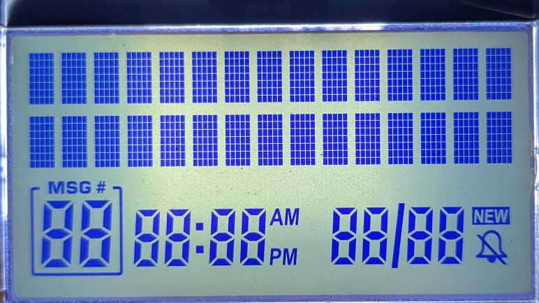
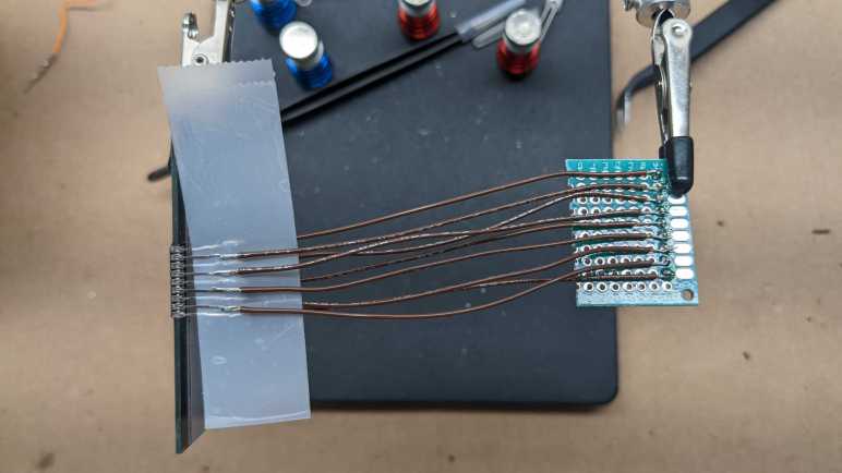
My Saleae Logic 8 listening to the communication traffic on the I2C data bus of an AT&T CL84209 cordless phone headset heard thousands of messages within ten seconds of startup, addressed to ten different device addresses. I only cared about the messages related to its LCD screen and, fortunately, that data stood out and now I know this LCD is an I2C device with address of 0x3E.

Curious if knowing the I2C address will help me find more information on this LCD, I went online and… didn’t have much luck. Adafruit organizes a list of their I2C product addresses, but as of writing there’s nothing listed for 0x3E. I found the JHD1313 LCD module online, whose AiP31068 controller is an I2C device on address 0x3E. This chip is controlled with a series of command words, which is a control byte followed by a data byte. Different from the pattern I see on my Saleae decoded data, where character data is sent consecutively without command bytes in between. (Also, the datasheet annoyingly doesn’t give its I2C device address in hexadecimal or decimal form, only in binary form “011 1110” in the serial interface protocol chart.)

Empty-handed from this detour, I returned to my Python program parsing Saleae-decoded output. Out of 2569 captured messages, only 143 of them (5.57%) were addressed to 0x3E. This is a much more manageable number. Looking at that set, I found there were many two-byte messages and a few of the longer 18/19 byte messages.

The sequence of two-byte messages is almost identical throughout the capture, only difference is that the very first instance is one message shorter. (It omitted the final 0x00,0x02.) After that, the whole sequence repeats once every second. Lacking datasheet, I’m calling this the configuration sequence.

write to 0x3E ack data: 0x00 0x39 
write to 0x3E ack data: 0x00 0x1C 
write to 0x3E ack data: 0x00 0x70 
write to 0x3E ack data: 0x00 0x5F 
write to 0x3E ack data: 0x00 0x6C 
write to 0x3E ack data: 0x00 0x0C 
write to 0x3E ack data: 0x00 0x02 (Omitted from initial startup)

Shortly after this is sent, three lines of display data are sent. The capture included three variations. The first one is sent only once, immediately after the initial configuration sequence is sent:

write to 0x3E ack data: 0x80 0x81 0x40 0x20 0x20 0x20 0x20 0x20 0x20 0x20 0x20 0x20 0x20 0x20 0x20 0x20 0x20 0x20 
write to 0x3E ack data: 0x80 0xC1 0x40 0x20 0x20 0x20 0x20 0x20 0x20 0x20 0x20 0x20 0x20 0x20 0x20 0x20 0x20 0x20 
write to 0x3E ack data: 0x80 0x40 0x40 0x00 0x00 0x00 0x00 0x00 0x00 0x00 0x00 0x00 0x00 0x00 0x00 0x00 0x00 0x00 0x00 

The first two lines are all spaces, and the third line is all zeros. I interpret this as the “clear screen” for this LCD.

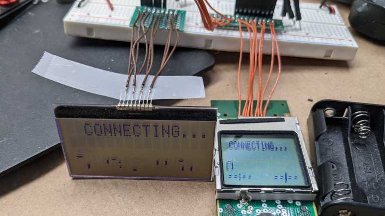
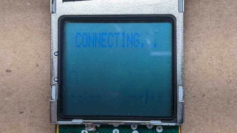
Afterwards, we have two variations of display data with “CONNECTING…” text. The first one:

write to 0x3E ack data: 0x80 0x81 0x40 0x20 0x43 0x4F 0x4E 0x4E 0x45 0x43 0x54 0x49 0x4E 0x47 0x2E 0x2E 0x2E 0x20 
write to 0x3E ack data: 0x80 0xC1 0x40 0x20 0x20 0x20 0x20 0x20 0x20 0x20 0x20 0x20 0x20 0x20 0x20 0x20 0x20 0x20 
write to 0x3E ack data: 0x80 0x40 0x40 0x00 0x00 0x10 0x02 0x01 0x04 0x00 0x10 0x00 0x04 0x01 0x00 0x02 0x10 0x04 0x00 

Differs from the second one by only a single bit in the third line, 0x00 vs. 0x10:

write to 0x3E ack data: 0x80 0x81 0x40 0x20 0x43 0x4F 0x4E 0x4E 0x45 0x43 0x54 0x49 0x4E 0x47 0x2E 0x2E 0x2E 0x20 
write to 0x3E ack data: 0x80 0xC1 0x40 0x20 0x20 0x20 0x20 0x20 0x20 0x20 0x20 0x20 0x20 0x20 0x20 0x20 0x20 0x20 
write to 0x3E ack data: 0x80 0x40 0x40 0x00 0x10 0x10 0x02 0x01 0x04 0x00 0x10 0x00 0x04 0x01 0x00 0x02 0x10 0x04 0x00 

This is consistent with handset LCD behavior blinking the “battery low” icon in the custom segmented LCD area. From here we can tell the first two lines are alphanumeric text, and the third line are bits for segmented LCD control where 0 is clear and 1 is active.

Looking at the screen, I see the battery icon blinking once a second. (Half second on, half second off.) Given this, I had expected to see the two variations of display data to alternate. Instead, it’s usually two of one style followed by one of the other. This mystery was solved once I looked at the timestamps: once every second, the configuration sequence is sent immediately followed by the current display state. Even if the display state hadn’t changed from the previous display update. In between these configuration sequences, the battery icon state is toggled every half second without sending the configuration sequence.

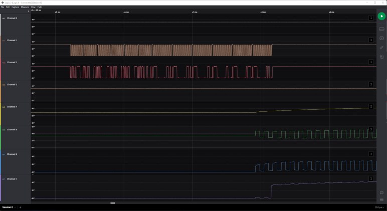
Thanks to Saleae Logic software and a bit of Python, I feel I’ve gained a working grasp of digital control communication for this LCD. I don’t know what any of those control flags individually mean, but I wouldn’t need to fully understand them if I just wanted to send alphanumeric data and toggle segments. Outside of these digital signal pins, there’s still the unknown of analog voltage pins. But looking at the timeline, I noticed an interesting correlation.