
This Form 1+ laser resin printer has a scorched galvanometer control board, and replacements are no longer available from FormLabs. I don’t have any background to make heads or tails of a laser galvanometer control board, but I might get a vague idea and learn something by examining its collection of components. Here’s a roll call based on markings on those chips.
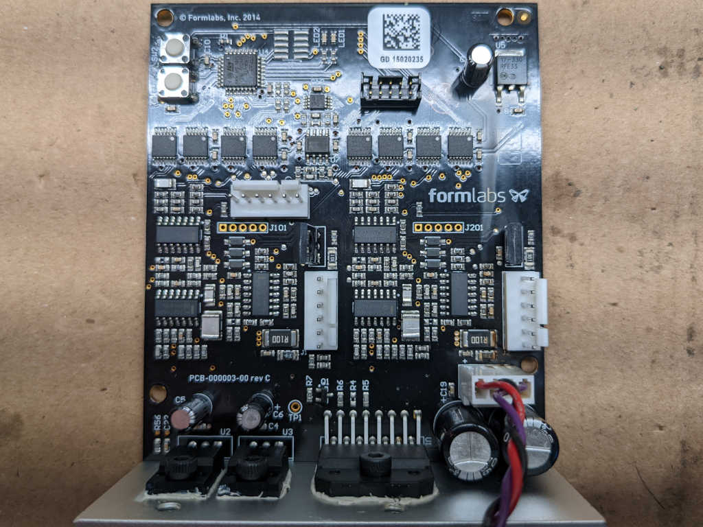
The board controls both X and Y axis galvanometers, probably why the middle section of this board a pair of identical assemblies.
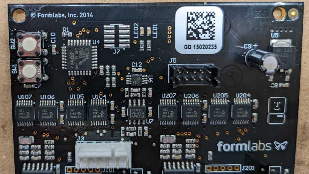
Starting from the upper left, component U4 looks to be the brains of this operation: a ST Microelectronics STM32F030K6T6 with its ARM Cortex-M0 core running at up to 48MHz.
U5 in the upper right is an On Semiconductor NCP1117, a low-dropout (LDO) voltage regulator marked with 17-33G indicating it outputs 3.3V. This would supply power to the STM32 and other 3.3V digital logic.
Back towards the centerline, U6 is a Microchip MCP4802 digital-to-analog converter (DAC) with dual 8-bit resolution channels controlled via SPI.
Just below that is U7, a TI TL032 dual-channel op-amp.
On either side of U7 is a collection of 8 chips, four on each side. (U104, U105, U106, and U107 on the left. U204, U205, U206, and U207 on the right.) They are all marked with Microchip logo and 41H51103, which I found to be a MCP41HV51 SPI-controlled digital potentiometer. In section 11.1 Package Marking Information of the MCP41HVx1 datasheet, 41H51103 is identified as MCP41HV51-103E/ST variant.
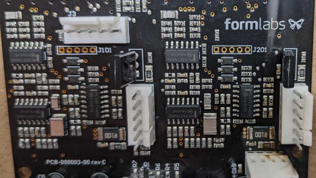
There are a lot of surface mount passives in the center section with two copies of the layout left and right. Each copy gets a trio of chips marked with On Semiconductor logo and MC33274ADG. These MC33274A chips are each a quad-pack of op-amps. Each side has an additional component that is mounted vertically so we only see their top here.

Going back to an earlier picture focused on the burnt and melted connector, we can see one of those vertical standing components clearly on the right. They are On Semiconductor BD139 NPN power transistors.
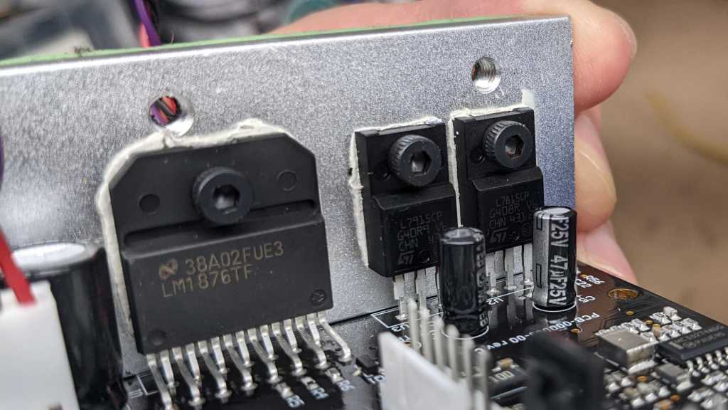
Three components are bolted to a heat sink at the bottom. To the left is a single Texas Instruments LM1876. It is a dual 20W audio power amplifier. Adjacent to that amplifier are a mirror pair of ST Microelectronics voltage regulators. The L79 negative voltage regulator accept up to -35V DC and output a regulated -15V DC. L78 is its symmetric positive voltage sibling, accepts up to +35V DC and output a regulated +15V DC.
Those components are major pieces of my “how did this board work” puzzle, but I’m still fuzzy on how they fit together. If I want more data, I’ll have to probe around while the system is powered up and I’m not entirely sure I want to do that.
