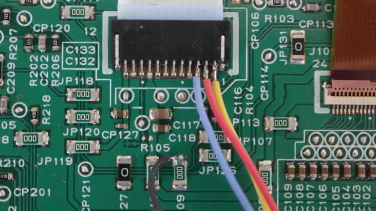
I’m using my Saleae Logic 8 logic analyzer to examine internal communication of a Canon Pixma MX340 multi-function inkjet. When the user plugs in the power cord, there was a tiny bit of internal activity even though nothing is visible to the user. I will now compare that against the communication traffic triggered by a user press on the power button.
I had hoped to see some of the same things I saw during power cord plug-in happen during turn on as well, as that would reinforce the observation they are critical to startup. Indeed, roughly 15ms after enable pin was raised, there was a two-byte report of 0x80 0x40 again. This makes me confident we can look for that as the control panel’s first “I’m awake!” response after being enabled.
About 9.2ms later (another match from earlier observations) another 0x80 0x40 was reported. But it started just after the main board sent its own two-byte sequence 0xFE 0xDC. During plug-in I saw the main board send the same 0xFE 0xDC sequence, but in that case it didn’t start until just after the second 0x80 0x40 report from the control panel. Conclusion: Timing of 0xFE 0xDC is not dependent on control panel’s second report.
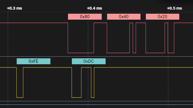
Since this 0xFE 0xDC transmission caught the control panel while it was in the middle of making its second 0x80 0x40 report, it appended its 0x20 acknowledgement immediately afterwards. Conclusion: the main board would not be confused if its 0xFE 0xDC transmission is immediately followed by a 0x40, it is still valid to send 0x20 acknowledgement afterwards.
After that exchange, there were twelve two-byte transmissions from the main board to the control panel, each acknowledged with a 0x20.
| Main board to control panel | Control panel acknowledgement |
|---|---|
| 0x0E 0xFD | 0x20 |
| 0x0D 0x3F | 0x20 |
| 0x0C 0xE1 | 0x20 |
| 0x07 0xA1 | 0x20 |
| 0x03 0x00 | 0x20 |
| 0x01 0x00 | 0x20 |
| 0x0E 0xFC | 0x20 |
| 0x04 0xD5 | 0x20 |
| 0x04 0x85 | 0x20 |
| 0x04 0x03 | 0x20 |
| 0x04 0xC5 | 0x20 |
| 0x04 0x34 | 0x20 |
Given that the control panel just woke up, these bytes probably set configuration registers on the NEC K13988 chip. I don’t know what they all do, but the first observable effect is in the reporting data sent by the control panel every 9.2ms. Before this exchange, it would send two bytes 0x80 0x40. After this exchange, it dropped the second byte and sent just 0x80. Two such reports were sent before the next main board transmission, 0x04 0x74.
20ms later, a set of four two-byte transmissions were sent.
| Main board to control panel | Control panel acknowledgement |
|---|---|
| 0x04 0xF4 | 0x20 |
| 0x04 0x44 | 0x20 |
| 0x04 0x81 | 0x20 |
| 0x04 0x04 | 0x20 |
Again I don’t know what these mean exactly, but I noticed these all started with 0x04 as their first byte. Looking at the previous sequence of twelve bytes, the final five also started with 0x04 but none of the second bytes repeated.
After that, all was quite for about 109ms, just the regular report of 0x80 from the control panel every 9.2ms. Then the main board sent one more two-byte sequence: 0x04 0x42. After that was acknowledged, I saw a pattern I recognized: a blast of bytes to update LCD screen content starting with 0x04 0x4D, 0x04 0xC8, etc. After the sequence completed, there was one more two-byte sequence I hadn’t seen before: 0x04 0xF5. Adding to the pile of unknowns: why did this screen update needed a 0x04 0x42 preamble and 0x04 0xF5 appendix?
Another 112ms later, the main board sent 0x0E 0xFD.
Another 19ms after that, there was another blast of LCD screen content. This time, there were no 0x04 0x42 preamble, nor 0x04 0xF5 suffix.
It was a relatively long wait of 669ms until the next main board transmission: 0x0E 0xFF acknowledged with 0x20. 145us later, 0x0E 0xFF was sent again and acknowledged again. More unknowns: Why did this need to be sent twice in rapid succession?
Whatever its purpose, another LCD screen update followed 65ms later. No preamble for this one, but it was followed by 0x0E 0xFF yet again.
An even longer 1695ms (1.7 seconds) later, there was another LCD screen update transmission. This had had no extra prefix or extra suffix and, after this transmission completed, I saw only the 9.2ms button matrix report for several seconds. I stopped the capture and trimmed the data to end after this transmission.
Summary
When the user presses the power button, there were a little over three seconds of activity of data sent by the main board, each acknowledged by the control panel with 0x20:
- (24ms)
- 13 two-byte sequences.
- (17ms)
- 0x04 0x74
- (20ms)
- 4 two-byte sequences.
- (109ms)
- 0x04 0x42
- LCD screen update
- 0x04 0xF5
- (112ms)
- 0x0E 0xFD
- (19ms)
- LCD screen update
- (669ms)
- 0x0E 0xFF twice
- (65ms)
- LCD screen update
- 0x0E 0xFF
- (1695ms)
- LCD screen update
- (steady state)
There are four LCD screen update sequences in this capture, but the user only sees three distinct display updates. Given there was only 115ms between the first and second update, that first update didn’t stay on screen long enough to convey any useful information for human eyes. Hypothesis: the first update is a “clear screen” sequence, something to investigate later. Right now I want to look at the mirror transition of dropping from powered-on to standby.
This teardown ran far longer than I originally thought it would. Click here to rewind back to where this adventure started.
