SATA Optical to 2.5″ Drive Adapter

I dusted off an old Dell Optiplex 960 for use as my TrueNAS replication backup target. The compact chassis had a place for my backup storage 8TB 3.5″ HDD extracted from a failed USB enclosure, which is good. But I also need a separate drive for Ubuntu operating system, and that’s where I ran into problems. There was an empty 3.5″ bay and a SATA data socket available on the motherboard, but the metal mounting bracket was missing, and power supply had no more SATA power plugs.

As an alternative plan, I thought I would repurpose the optical drive’s location. Not just its SATA data and power plugs, but I could also repurpose physical mounting bracket with an optical drive shaped caddy for a 2.5″ SATA drive. (*) It wasn’t a perfect fit but that was my own fault for ordering the wrong size.

Examining the caddy after I opened its package, I saw this oddly bent piece of sheet metal. Comparing against the DVD drive, I don’t think it’s supposed to bend like that. I can’t tell if it was damaged at the factory or during shipping, either way metal was thin and easy to bend back into place.

Also comparing against the DVD drive, I realized I bought the wrong size. It didn’t occur to me to check to see if there were multiple different sizes for laptop DVD drives. I bought a 9.5mm thick caddy (*) when I should have bought something thicker possibly this 12.7mm thick unit.(*) Oh well, I have this one in hand now and I’m going to try to make it work.

To install this caddy in an Optiplex 960 chassis, I need to reuse the sheet metal tray currently attached to the DVD drive.

One side fit without problems, but the other side didn’t fit due to mismatched height. This is my own fault.

There’s a mismatch in width as well, I’m not sure this was my fault. I understand the different form factors to be the same width so this part should have lined up. Oh well, at least it is easier to deal with a ~1mm too narrow adapter because one ~1mm too wide wouldn’t fit at all.

There were slots to take the DVD drive’s faceplate. This is for aesthetics so we don’t leave a gaping hole, the eject button wouldn’t work as it is no longer a DVD drive. Unfortunately, faceplate mounting slots didn’t match up, either. This might also be a function of the wrong height, but I’m skeptical. I ended up using the generic faceplate that came with the caddy.

Forcing everything to fit results in a caddy mounted crookedly.

Which resulted in a crooked facade.

Aesthetically speaking this is unfortunate, I should have bought a taller caddy (*) but functionally this unit works fine. The SSD is securely mounted in the caddy, which is now securely mounted to the chassis. And even more importantly, SATA power and data communication worked just fine, allowing me to install Ubuntu Server 22.04 LTS on an old small SSD inside the caddy. And about that old SSD… freeing it up for use turned out to be its own adventure.


(*) Disclosure: As an Amazon Associate I earn from qualifying purchases.

Dusting Off Dell Optiplex 960 SFF PC

After two years of use, my USB3 external 8TB backup drive stopped responding as an external disk. I took apart its enclosure and extracted a standard 3.5″ hard disk drive which seems OK in perfunctory testing. In order to continue using it for TrueNAS replication backup, I’ll need another enclosure. I briefly contemplated getting an USB3 SATA enclosure that takes 3.5″ drives (*) but I decided to use an entire computer as its enclosure: I have an old Dell Optiplex 960 SFF (small form factor) PC collecting dust and it would be more useful as my TrueNAS replication backup machine.

Dell’s Optiplex line is aimed at corporate customers, which meant it incorporated many design priorities that weren’t worth my money to buy new. But those designs also tend to live well past their first lives, and I have bought refurbished corporate Dells before. I’ve found them to be sturdy well-engineered machines that, on the secondhand market, is worth a small premium over generic refurbished PCs.

There’s nothing garish with exterior appearance of an Optiplex, just the computer equivalent of professional office attire. This particular machine is designed to be a little space-efficient box. Office space costs money and some companies decide compactness is worth paying for. Building such a compact box required using parts with nonstandard form factors. For a hobbyist like me, not being able to replace components with generic standard parts is a downside. For the corporate IT department with a Dell service contract, the ease of diagnosis and servicing is well worth the tradeoff.

This box is just as happy sitting horizontally as vertically, with rubber feet to handle either orientation.

Before it collected dust on my shelf, this computer collected dust on another maker’s shelf. I asked for it sometime around the time I started playing with LinuxCNC. I saw this computer had a built-in parallel port, so I would not need an expansion card. (Or I can add a card for even more control pins.) The previous owner said “Sure, I’m not doing anything with it, take it if you will do cool things with it.” Unfortunately, my LinuxCNC investigation came to a halt due to pandemic lockdown and I lost access to that space. TrueNAS replication target may not be as cool as my original intention for this box, but at least it’s better than collection dust.

Even though the chassis is small, it has a lot of nice design features. The row of “1 2 3 4” across the front are diagnostics LEDs. They light up in various combinations during initial boot-up so, if the computer fails to boot corporate IT tech support can start diagnosing failure before even opening up the box.

Which is great, because opening up the box might be hindered by a big beefy lock keeping the side release lever from sliding.

And if we get past the lock and open the lid, we trip the chassis intrusion detection switch. I’ve seen provision for chassis intrusion detection in my hobbyist-grade motherboards, but I never bothered to add an actual intrusion switch to any of my machines. Or a lock, for that matter.

Once opened I find everything is designed to be worked on without requiring specific tools. This chassis accommodates two half-height expansion cards: One PCI and one PCI-Express. On my PCs, expansion endplates are held by small Philips-head screws. On this PC, endplates are retained by this mechanism.

A push on the blue button releases a clamp for access to these endplates.

Adjacent to those expansion slots is a black plastic cage for 3.5″ Hard drive.

Two blue metal clips release the cage to flip open, allowing access to the hard drive. This drive was intended to be the only storage device hosting operating system plus all data. I plan to install my extracted 8TB backup storage drive in this space, which needs to be a separate drive from the operating system drive, so I need to find another space for a system drive.

Most of the motherboard is visible after I flipped the HDD cage out of the way. I see three SATA sockets. One for the storage HDD, one for the DVD drive, and an empty one I can use for my system drive. Next to those slots is a stick of DDR2 RAM. (I’m quite certain Corsair-branded RAM is not original Dell equipment.) Before I do anything else with this computer, I will need to replace the CR2032 coin cell timekeeping battery.

A push on the blue-stickered sheet metal button released the DVD drive. Judging by scratches, this DVD drive has been removed and reinstalled many times.

Putting the DVD drive aside, I can see a spare 3.5″ drive bay underneath. This was expected because we could see a 3.5″ blank plate in the front of this machine, possibly originally designed for a floppy disk drive. The good news is that this bay is empty and available, the bad news is that a critical piece of hardware is missing: This chassis is designed to have a sheet metal tray for installing a 3.5″ drive, which is not here.

I can probably hack around the missing bracket with something 3D-printed or even just double-sided tape. But even if I could mount a small SSD in here, there are no spare SATA power connector available for it. This is a problem. I contemplated repurposing the DVD drive’s power and data cables for a SSD and found adapters cables for this purpose. (*) But under related items, I found a product I didn’t even know existed: an optical-to-hard drive adapter (*) that doesn’t just handle the power and data connectors, it is also a mechanical fit into the optical drive’s space!


(*) Disclosure: As an Amazon Associate I earn from qualifying purchases.

Seagate Backup+ Hub External Drive 8TB (SRD0PV1) Teardown

I’ve owned and taken apart several USB external hard drives to extract their standard form factor SATA hard drive within. Today another drive shall undergo an extraction process. This is a Seagate Backup Plus Hub (SRD0PV1) I had used to back up my TrueNAS disk array. I used a Raspberry Pi as TrueNAS replication host and this drive as storage. I paid a few extra bucks for the version with an integrated USB hub hoping to power my Raspberry Pi from one of the ports and simplify my wiring. Unfortunately, I learned that when the drive initially spins up, all power goes to the drive and these USB ports become momentarily disconnected. Shutting down the Pi sank my plan. I shrugged, chalked the few extra bucks to lesson learned and ignored its integrated USB ports. I powered my Pi conventionally and used the drive for TrueNAS replication back up storage. That daily backup setup worked for about two years before TrueNAS started reporting replication failures: “Device not found.” Where did it go? Looks like my Raspberry Pi would acknowledge the drive existed as a USB device but couldn’t use it as one.

Running Ubuntu’s dmesg command and querying for all the lines that have USB in it, I found a trail ending with an error message “Cannot enable. Maybe the USB cable is bad?” Following that advice, I tried several different cables but that didn’t make a difference, so it wasn’t the cable. I tried plugging the drive into my Windows machine with similar results: New USB device? Yes. New hard drive? No.

Thus it was time for another hard drive shucking session. Since my TrueNAS array is running well, the data within isn’t critical right now. But it’s a low-pressure opportunity to learn if my data backup would survive such an episode of hardware failure.

I found no external fasteners (not even under its rubber feet) so I started attacking visible seams with iFixit opening pick and opening tool.

After a symphony of snapping sounds announcing death of many plastic clips, top lid came free. We can see a Seagate BarraCuda 3.5″ HDD. It is from their “Compute” product line for general personal storage usage. Usually with a two-year warranty, so we’re right on time.

Speaking of warranty, there was an interesting piece of text on the label that I don’t think I’ve seen elsewhere before. “HDD sold as component of OEM solution and not for resale. The product warranty does not cover HDD if removed from OEM solution.” If the warranty hadn’t already expired, I guess I’ve just voided it.

Many more snapping of clips later, the external enclosure has been separated into three plastic pieces: top, bottom, and a frame sandwiched between them.

RIP, plastic clips.

Vibration dampening rubber knobs sit between the external frame and screws fastening the HDD to a folded sheet metal tray.

Once those screws were removed, the drive could be slid off the tray. I was surprised to see such a large expanse of circuit board; I had expected two small boards with a ribbon cable to bridge them.

Removing two screws allowed the circuit board to be removed. All physical connectors (SATA, power, USB) are on this side, as are a few through-hole electrolytic capacitors.

The other side is sparsely populated with surface-mount components.

I didn’t see any visible signs of damage that might explain why Ubuntu “cannot enable” this device. Not that I would necessarily know how to fix it, anyway. This was just for curiosity. I might as well look around now that I have this in my hands.

I noticed three identical copies of a circuit, but beyond that, I don’t know what it does. Why would the circuit board for an external hard drive need three of something?

The largest chip on this board is a GL3520 by Genesys Logic, a Taiwan company specializing in USB solutions. The GL3520 is no longer listed on their website, but their GL3523 (which I infer to be its successor based on model number) is listed as a USB3 hub controller. This is consistent with integrated USB hub functionality.

The next largest chip is the ASM1153 by ASMedia, another Taiwan company. ASM1153 is a USB to SATA bridge and its presence is completely expected within an external USB hard drive product.

But now with the enclosure removed, this Seagate BarraCuda Compute 8TB drive has been transferred to the PC with a Rosewill hard disk drive cage so it is now an internal drive. It was successfully detected as a SATA device, and by running “zpool import” I was able to mount it to my Ubuntu filesystem. I copied a few files as tests, and they all seemed intact. Then I ran “zpool scrub“, and no errors were detected. I take this to mean that my data has survived which is great news. I want to keep using it as my TrueNAS replication backup, but I don’t want to dedicate my PC tower to this task. Fortunately, I have an old Dell Optiplex 960 that should suit.

Window Shopping: GMKtec NucBox3 Mini PC

A Newegg advertisement sent me down a rabbit hole of tiny little desktop PCs with full x86-64 processors. I knew about Intel’s NUC, but I hadn’t realized there was an entire product ecosystem of such small form factor machines built by other manufacturers. The one that originally caught my attention was distributed by several different companies under different names, I haven’t figured out who made it. But that exploration took me to GMKtec which is either their manufacturer, or a distributor with a sizable collection of similar products built by different manufacturers. The product that originally caught my attention is listed as their “NucBox5” (company website listing and Amazon link *) but I actually found their “NucBox3” (company website listing and Amazon link *) to be a more interesting candidate for my Sawppy Rover’s ROS brain. Both products have a Gigabit Ethernet wired networking port that I demand for resistance against RF interference, but beyond that, their respective designs differ wildly:

First the bad news: the NucBox 3 has an older CPU, the Celeron J4125 instead of the Celeron N5105. But comparing them side-by-side, it looks like I’d be giving up less than 10% of peak CPU performance. There is a huge (~50%) drop in GPU performance, but that doesn’t matter to Sawppy because most of the time its brain wouldn’t even have a screen attached.

A longer list of good stuff balances out the slower CPU:

  • RAM on the NucBox 3 is a commodity DDR4 laptop memory module. That can be easily upgraded if needed, unlike the soldered-in memory on the NucBox 5.
  • They both use M.2 SSDs for storage, but the NucBox 3 accommodates popular 2280 form factor instead of a less common 2245 size used by NucBox 5.
  • The SSD advantage was possible because NucBox 3 has a different shape: is wider and deeper than a NucBox 5, but not as tall. Designed for installation on a VESA 100×100 mount, it will be easier to bolt onto a rover chassis.
  • Officially, NucBox 3 is a fan-less passively cooled machine whereas the NucBox 5 has a tiny little cooling fan inside. (Which I expect to be loud, as tiny cooling fans tend to be.) Given that these are both 10W chips, I doubt NucBox 3 has a more effective cooling solution, I think it is more likely that the design just lets the chip heat up and throttle itself to stay within thermal limits. This would restrict its performance in stock form, but it also means it’ll be easy for me to hack up a quiet cooling solution if necessary.
  • NucBox 5 accepts power via USB-C, which is getting easier and easier to work with. I foresaw no problems integrating it with battery power onboard a Sawppy rover. But the NucBox 3 has a generic 5.5mm barrel jack for DC input power, and I think that’ll be even easier.

A NucBox3 costs roughly 80% of a NucBox5 for >90% of the performance, plus all of the designed tradeoff listed above are (I feel) advantages in favor of the NucBox3. I’m sold! I placed an order (*) and look forward to playing with it once it arrives.


(*) Disclosure: As an Amazon Associate I earn from qualifying purchases.

Window Shopping: Mystery Mini PC of Many Names

An interesting item came to my attention via Newegg marketing mailing list for discounts: an amazingly tiny Windows PC. My attention was captured by listing picture showing its collection of hardware ports. Knowing the size of an Ethernet port and HDMI port we can infer this is an itty-bitty thing. Newegg’s specific sale item was generically named “Mini PC” with an asking price of $200. I’m not entirely sure the thing is real: all the images look perfect enough I couldn’t tell if they’re 3D renderings or a highly retouched product photos.

I looked at the other listings by the same vendor “JOHNKANG” and saw several other generically named devices ranging from laptops to external monitors. There were no other similar products, so I think JOHNKANG is a distributor and not the manufacturer of this palm-sized wonder. If JOHNKANG is a US distributor for such merchandise, I guessed they probably have an Amazon listing as well. Sure enough, they have it listed on Amazon also at $200(*) at time of writing. Unlike the Newegg listing, the Amazon listing included this exploded-view diagram showing internals and capabilities.

That’s… pretty darned good for $200! With an Intel Celeron N5105 processor, I see a machine roughly equivalent to capabilities of a budget laptop but without the keyboard, screen, or battery. Storage size is serviceable at 256GB and can be swapped out with another M.2 SSD, though in a less common 2242 format which is shorter than the popular 2280. Its 8GB of RAM are soldered and not easily expandable, but 8GB is more than sufficient for this price point.

A few features distinguish this tiny PC from equivalent-priced laptops, starting with its dual HDMI port where laptops only have one. That might be important for certain uses, but I’m more interested in its wired Gigabit Ethernet port and that it runs on USB-C power input. This machine appears to check off all of my requirements for a candidate Sawppy Rover brain. It’s a pretty good candidate for running ROS slotting just below an Intel NUC in capability but compensates for that with a lower price and smaller physical size. Heck, at this size it is starting to compete with Raspberry Pi and might even fit in a Micro Sawppy.

I found no make or model number listed, which is consistent with a distributor that really doesn’t want us to comparison shop against anyone else who might be distributing the same product for less money. If I want hard details, I might have to buy one and look over the hardware for hints as to who built it. Still, searching for “Mini PC” and “MiniPC” with N5105 CPU found this eBay listing of a used unit with Rateyuso branding. Then I found this AliExpress listing with ZX01 as model name. That AliExpress listing is a mess, showing pictures of several other different mini PCs. Not confidence inspiring and definitely turned me off of buying from that vendor. However, the “ZX01” model name was useful because it led me to this page, which linked to a Kickstarter project that has apparently been taken down due to intellectual property dispute.

Performing an image search using the suspiciously perfect picture/render found the GMKtec Nucbox5(*) which appears to be the same product but with “GMKtec” stamped on top. Looking at the Amazon storefront for GMKtec (*) I see many other small form factor PCs without any family resemblance between their industrial designs. My hypothesis is that GMKtec is a distributor as well, but they have built up a collection of products from different manufacturers and that’s why they all look different. I thought this was encouraging. It implies experience and knowledge with the ecosystem of tiny PCs, offering a breadth of products each making a different tradeoff. I looked over their roster and found one more to my taste.


(*) Disclosure: As an Amazon Associate I earn from qualifying purchases.

Google OAuth Test Tokens Expire Weekly

I know I have a lot to learn about network security, acronyms like CORS and CSRF are just a start. Another name I’ve come across is OAuth, which looked very complicated. Some critics say its complexity was by design, cynically describing OAuth as a system designed by enterprise security consultants to sell more consulting services. I don’t know how true that is, but just from touching its edge I can confirm it is even more complicated than it looked.

My introduction was via Home Assistant, which was primarily designed to keep everything in my home and would have no need for OAuth. Pragmatically, though, it also makes effort to connect to cloud-based services, even though that is no longer keeping everything in my home. In order to connect to Google/Amazon/etc. there needs to be an internet-accessible entry point to a Home Assistant instance. It’s possible to do everything ourselves, but the easier way is to pay Nabu Casa for a Home Assistant Cloud account to bridge between public internet and private home network. Such payment also supports development of Home Assistant, which I’m happy to do.

My first test for Home Assistant Cloud was to connect to my Nest thermostat. Home Assistant has an integration for Google Nest, and it was implemented in a way to leave a lot of control in the user’s hands. Instead of something that suspiciously sucks up our Google credentials, we get instructions on how to use our own Google credentials to grant very specific and narrow access to Home Assistant Cloud. The upside is that Nabu Casa doesn’t get to say how that access is granted. The downside is that we have to deal with everything ourselves, and that meant dealing with OAuth.

Following instructions for integration setup means setting up a Google developer account and logging into our Google Cloud services console to set up a new project to communicate with Home Assistant. This is not very user-friendly but reflects the developer-oriented origins of Home Assistant. One of the steps told us to “Publish App” because if we don’t, the project status will stay “Testing”. “Make sure the status is not Testing, or you will get logged out every 7 days.

When I click “Publish App” I was told my app requires verification which requires:

  1. An official link to your app’s Privacy Policy
  2. A YouTube video showing how you plan to use the Google user data you get from scopes
  3. A written explanation telling Google why you need access to sensitive and/or restricted user data
  4. All your domains verified in Google Search Console

A privacy policy? A YouTube video? A written explanation for Google? I didn’t want to do all that just to access my Nest thermostat from Home Assistant! Google OAuth API Verification is a whole bag of worms, even their FAQ page is a long slog of a read.

So, I bailed.

But this meant my Home Assistant OAuth token expires after a week. (“A Google Cloud Platform project with an OAuth consent screen configured for an external user type and a publishing status of “Testing” is issued a refresh token expiring in 7 days.“) After that, I would have to manually renew it. This is far from ideal, and a poor first impression for working with OAuth. Maybe I’ll be less hostile to OAuth once I get some experience with it, but this first impression certainly doesn’t motivate me to do that anytime soon.

Web Dev Alphabet Soup: CORS and CSRF

After a helpful comment helped me find documentation on the no-longer-mysterious AS7341 SMUX (sensor multiplexor) I went to learn more about another mystery I stumbled across as a beginner web developer: CORS (cross-origin resource sharing.) Why does CORS policy exist? After a bit of poking around, I believe the answer is to mitigate a type of attack under the umbrella of CSRF (cross-site request forgery.)

When developing my AS7341 web app, I had the AS7341 accessible via a HTTP GET on my ESP32 and thought I could develop the HTML interface on my desktop machine. But when my desktop-served JavaScript tried to query my ESP32, I was blocked by browser CORS policy. By default, JavaScript served from one server (my desktop) is not allowed to query resources on another (my ESP32.)

Reading various resources online, I learned I could set my ESP32’s HTTP response header “Access-Control-Allow-Origin” to a wildcard “*” to opt out of CORS protection. But that’s merely a “make the error go away” kind of recommendation. I know CORS is security related, but I don’t understand the motivation. What security problem does CORS prevent? Without knowing the motivation, I don’t know what I am opening up by setting “Access-Control-Allow-Origin : *” In my web app, I started out cautiously by only setting that header when I’m developing the HTML UI, serving from my desktop to query my ESP32. In “production”, my ESP32 will serve the HTML and would not need “Access-Control-Allow-Origin : *” in the header to query itself, so that header is absent.

Is that the right thing to do, or is that being overly cautious? I set out to learn more. Curiously, reading MDN and other resources give me information about HOW CORS works, but not a lot about WHY CORS exists. I guess CORS documentation assume the reader already knows! Based on that fact, I know I am looking for a relatively common website security issue that is now considered basic knowledge by network professionals.

Another data point is the fact that CORS is only applicable to HTTP queries from JavaScript running in the browser. From a command line on my desktop, I can use the “curl” tool to query my ESP32 and CORS does nothing to block that. My browser on my desktop can query the endpoint directly and that is not blocked by CORS policy, either.

Things didn’t make much sense until I found a key piece of information: HTTP request sent from a browser’s JavaScript runtime not only sends the URL and its parameters, but the browser would also attach all cookies set by that host. These cookies may contain user authentication (the “Keep me logged in” checkbox) and it makes sense such capability shouldn’t be available to just any piece of JavaScript served by random hosts. Knowing this fact and knowing the kind of abuse such code can cause eventually led me to a category of security attacks known as CSRF (cross-site request forgery.)

Once I understood CORS is here to mitigate a subset of CSRF attacks, I could look at my ESP32 AS7341 access endpoint and decide CSRF is not a problem here. Setting “Access-Control-Allow-Origin : *” does not open me up to security nastiness, so my ESP32 sketch sets that header all the time now not just during development. This is a handy bit of knowledge, but it merely scratched the surface of web security. Another item I found to be big and intimidating is OAuth.


Code for this project is publicly available on GitHub

AS7341 Project Postscript: SMUX Mystery Solved

I’ve wrapped up version 1.0 of my AS7341 interaction web app project with some ideas for future improvements, but I learned of a big one after I wrote up my project. When an earlier post in my AS7341 series “Sample Code Gave Incomplete Picture of AS7341 SMUX Configuration” was published, there was a comment by [Sebastian] telling me that I’ve overlooked the “Tools & Resources” tab of AMS AS7341 product page.

[Sebastian] is correct! There were several large ZIP file downloads under “Resources” of type “Evaluation Software”. Their descriptions line up with several AMS demos for this sensor. I probably dismissed them as irrelevant as I don’t have the corresponding AMS concept demonstration hardware. But [Sebastian] didn’t make the same mistake. Thanks to his investigation, I’ve been prompted to look inside and found that, in additional to demo-specific resources, there are subdirectories with reference resources including everything I complained was missing:

  • Windows application installer, likely for AMS AS7341 GUI software mentioned in calibration Application Note. (I didn’t install on my own computer.)
  • Excel spreadsheet also mentioned in calibration Application Note.
  • Calibration Application Note along with a few other Application Notes.
  • Most importantly: an Application Note on SMUX configuration details!

The gold nugget found within the ZIP file is AMS Application Note AN000666. “SMUX Configuration: How to Configure SMUX for Reading Out Results.” The precise location probably varies from file to file, but for the file I examined (AS7341_EvalSW_ALS_v1-26-3) it was under subdirectory “Documents”/”application notes”/”SMUX”

The key piece of information I had been missing earlier is the concept of mapping AS7341 sensor array to pixel IDs. These pixel IDs are not sequential or regular in any pattern I can decipher, and many pixel IDs are unused. I suspect these ID assignments made sense for reasons important to the engineering team that laid out this implementation on silicon wafers. Between their seemingly random order and the fact roughly half of the IDs were just unused, it was no wonder I failed to reverse-engineer this information from sample code.

But with this Application Note as reference, we now have information in hand to create SMUX configurations to best suit future projects. This is wonderful. Thanks, [Sebastian]! It’s a weight off my shoulders as I proceeded to learn about other mysteries.

AS7341 Project Future Enhancements

With my AS7341+ESP32 assembly all tidied up, alongside my web app project for interacting with them, I think this is a good point to declare version 1.0 complete and move on to something else. Naturally I have more ideas, but today I’m just going to write them down as ideas for later.

Color Accuracy

The most obvious point of improvement is a better translation from detected wavelengths to human-perceived color. I think this would require at least a few days of study (possibly more) before I can be conversant in the topic and maybe understand that Python code sample I found.

Beyond the theoretical math, there are hardware component to better color: the AS7341 has many additional capabilities that I have not used in my little exploratory app. While the eight sensors for specific wavelengths get the attention, the other sensors weren’t there just for fun. They also have a role in color accuracy as per AS7341 application node on color calibration. Those channels provide information on various distortions that may be affecting those eight wavelength sensors.

The clear channel shows the sensor response without a color filter, and the NIR channel shows raw silicon sensor response without even an infrared filter. When any of these sensors return a strong reading, that means enough of their respective types of light are likely “bleeding” into the other color sensors. Flicker detection is likewise also involved because flickering light patterns would impact sensor readings. All of these factors should need to be compensated before feeding into color space conversion.

Temperature Compensation

I haven’t used AS7341’s temperature compensation feature beyond its default behavior of running once upon powerup. Ambient temperature changes would affect sensor behavior, which is true of all sensors. Or to paraphrase what I’ve heard from veteran embedded engineer Elicia White: “Every sensor is a temperature sensor. Some even sense other things.”

Auto Gain Control

A little tangential to the topic of color accuracy, this sensor seems to have some sort of auto gain control to ensure sensors get a good range of values without going too far into saturation. Ideally, I can add an “Auto Gain” checkbox to my app and let the sensor take care of gain control automatically, but that isn’t as easy as it looked at first glance. This feature was not exposed in the Adafruit library and my effort to explore it with twi_nonblock API produced behavior I didn’t understand.

Web App Evolution

Orthogonal to anything I might do to improve AS7341 performance, I might choose to evolve just the web app itself. This first version was written directly in HTML/CSS/JavaScript, the only library I used was Chart.js to plot the bar graph. This process is fine for a simple app but will get more cumbersome for larger projects. So even though this app is fine for its scale, I might use it as “Hello World” exploration of tools that help manage larger projects. Like learning how to use NPM to manage dependencies like Chart.js. Or using TypeScript to tame some of JavaScript’s wild and annoying sides. Or convert it to use an application framework like Angular. That would be sheer overkill for such a small app, but I have big web app project ideas and I need someplace small to start learning.

ESP32 Evolution

Or I might focus on the ESP32 side of things. Top of the list here is using it as a learning project for ESPAsyncWebServer, which has more of the features I might want over the current basic WebServer implementation. Before that, though, I’ll probably switch over to using PlatformIO so I can upload HTML/CSS/JavaScript files to SPIFFS and serve from there, instead of the current unnecessarily cumbersome process of converting them over to hex values in a header file.

Platform Migration

Or a future path would not involve the web app at all. It’s totally possible for a future project idea to be done entirely onboard the ESP32, porting my browser-side JavaScript code to C on the ESP32. It all depends on what motivates me to create enhancements in the future.

Which may be triggered by something like discovering information I had mistakenly overlooked.

Compact Assembly of AS7341 and ESP32 Boards

Once I implemented a visual warning for AS7341 sensor saturation, I’ve completed a decent baseline set of features. Enough for me to declare version 1.0 is complete. I tidied up the source code with comments and license headers, now I will tidy up the hardware side as well. During development I used what I built at the start of this project, with my ESP32 mini dev board and AS7341 breakout board connected by a pre-crimped JST-SH cable(*) mechanically compatible with Adafruit’s STEMMA QT form factor. I thought the cable would give me flexibility in moving the AS7341 around, but it has just been a huge hassle with it dangling and flopping about.

For experiments in portability, I taped both components to a USB power bank. This worked well enough and taught me I prefer having everything as a single unit. I will rebuild my sensor package into a single compact form.

I unsolder the STEMMA QT-compatible JST-PH cable because I’m going to skip the cable and put these two modules back-to-back. I cut up an expired credit card to place between them as insulation. Since I would only need short sections of wire, I dug up a short cutoff piece of wire that was probably from a resistor.

SCL and SDA pins are connected straight through. Ground is almost as straightforward and handled with a short S-shaped length. Power has to come from the opposite side, though, so I used actual wire with insulation to connect to 3.3V power.

Once in place, I can power the ESP32 with a small adapter sold as an USB OTG adapter(*) but it also works as a zero-length USB cable.

Plugging everything in together, I have an AS7341 sensor mounted to the back of my ESP32 dev board, which is plugged in to a USB power bank serving as a handle. A nice small compact and portable setup, with nothing flopping about.

After a quick test run to verify everything still works correctly, I protected the circuit board assembly with clear heat-shrink tubing. (*) Or at least, it is clear to my eyes. It seems to affect AS7341 sensors readings somewhat, so it is not completely transparent across all wavelengths. In order to remove this interference, I cut a small window to ensure sensor has unobstructed view. This completes version 1.0 of my AS7341 project, but before I move on I wanted to write down ideas of what I might do later.


(*) Disclosure: As an Amazon Associate I earn from qualifying purchases.

Sensor Saturation Warning as Final V1 Feature of My AS7341 App

It’s been fun playing with my AS7341 interactive UI web app, seeing what the sensor sees and what the app guesses my eyes would see. They’re similar but rarely agree, as should be expected of a quick hack job. Occasionally I would see something wildly inaccurate, and it would take a few seconds for me to realize the problem: one or more AS7341 channels had hit their saturation (ADCfullscale) values. This “peg the scale” value (a.k.a. “off-scale high”) is no longer accurate. In photography this causes overexposure.

Since the raw server response JSON is printed at the bottom of my app, I could see sensor values that are at their ADCfullscale value. But this means mentally calculating ADCfullscale (which isn’t always 65535) and comparing them against those printed numbers. I could do it, but I wouldn’t know to do it unless I suspect something is wrong with the output. I want notification of sensor saturation whenever it happens, even (or especially!) when the result looks reasonable but are actually wrong.

The JavaScript code to detect saturation on a sensor channel was straightforward and can be performed in a loop over values for sensors F1-F8. Though it’s more likely to happen on Clear or NIR first, so I checked those as well. But then I had to show the result in a way that I would notice.

My first modification was to change the header text for server response JSON. Normally displaying “Sensor data OK” but switch to “Sensor saturation (overexposure) detected” as notification. This is an improvement, but I found I don’t always notice when my eyes are glued to the spectrum chart. To make sure I can’t miss it I changed the chart. Every bar was given a white border and, if saturation is detected, that border turns red. This was an improvement, but I might be focused on one channel and miss the fact another channel had saturated. As I understand it, when one channel is saturated, every reading is unreliable. So if this is a global problem, I’ll make the indicator global. The third modification changes every border to red if any channel had saturated. Now I can’t miss it!

With this sensor saturation notification feature, I think my AS7341 interactive web app is at a good place to wrap up for version 1.0. Before I put my sensor away, though, I wanted to make the hardware more compact and portable.


Code for this project is publicly available on GitHub

Approximate Color from AS7341 Spectral Data

It’s not going to win any design contests, but I’ve updated my AS7341 web app’s stylesheet so at least its layout is no longer confusing and no longer an embarrassing eyesore. It’s the first of several things I wanted to do for polish. My next challenge is to interpret AS7341 spectrum information into to a color hue a human eye would perceive from looking at the same thing. This is not a trivial conversion, as human color perception has been a long-running area of research. After a few minutes of trying to get my bearings on Wikipedia, I’ve reached the conclusion that doing a good job with my own implementation would take more time than I’m willing to spend on it.

What about somebody else’s implementation? A search for spectrum math library in JavaScript led me to a color picker control named Spectrum, which is not helpful to my current project. Looking on NPM, I found a CIE color conversion library, but I don’t see how to make it perform the type of conversion I seek. Casting my net wider than JavaScript, I found this article titled “Converting a spectrum to a colour” that opens with “This article presents a Python script to map a spectrum of wavelengths to a representation of a colour.” This is exactly what I want! Unfortunately, I struggled to understand the Python code, certainly not enough to convert it to JavaScript for my use. Maybe I can come back later to try again, but in the short term I will try a hack.

AS7341 datasheet tells us which wavelengths each sensors F1-F8 are designed to be sensitive to. Looking online, I found Academo’s “Wavelength to Colour Relationship” page that lets me input a wavelength and translate that to RGB value. Taking a table of RGB values for wavelengths corresponding to AS7341 sensors F1-F8, I added up each column: all the red in one value, all the green, then all the blue.

WavelengthRedGreenBlue
4151180237
445040255
4800213255
515312550
5551792550
5902552230
630255790
68025500
Sum10931065747

We see the highest sum for red, followed by green a bit behind, and blue is significantly lower. This is consistent with datasheet telling us the silicon underneath each wavelength filter is naturally more sensitive to red. Since white (and shades of gray) is represented by equal portions of red, green, and blue, getting there required boosting the blue-focused colors a bit to even things out. I didn’t put in rigorous mathematics to make them balanced since I don’t even know if this action makes sense in color science. As a quick hack, I used a spreadsheet and fiddled with numbers via trial and error. I found that if I multiplied 415nm by 1.72, 445nm by 1.6, and 480nm by 1.4, I would get red/green/blue within 1% of each other. From here I can multiply them by F1-F8 readings and calculate each of their contribution to red/green/blue channels and generate a color value.

This is an empirically derived formula with no basis in color science, but it does generate a color value that is vaguely in the right general ballpark. I piped that color into Chart.js to be used as my chart background color, following instructions on their documentation. This is most of what I wanted, and maybe the best I can do without investing the work to understand human color perception. Not great, but good enough for a quick hack project so I can move on to the next feature.


Code for this project is publicly available on GitHub

Rudimentary Stylesheet for AS7341 Web App

Writing a simple web app to interact with an AS7341 sensor, I initially focused on functionality. It didn’t much matter how it looked until I had basic parameter input and sensor value graphing output running. But now that I’ve got basic functionality in place, my attention turned to the CSS stylesheet. Up until this point my only item was to make input sliders full width of the window, as that helped me fine tune parameters and considered part of functionality. Now I’ll fill in the rest purely for aesthetics. I don’t need it to look gorgeous, but I did want to make sure it didn’t look embarrassing.

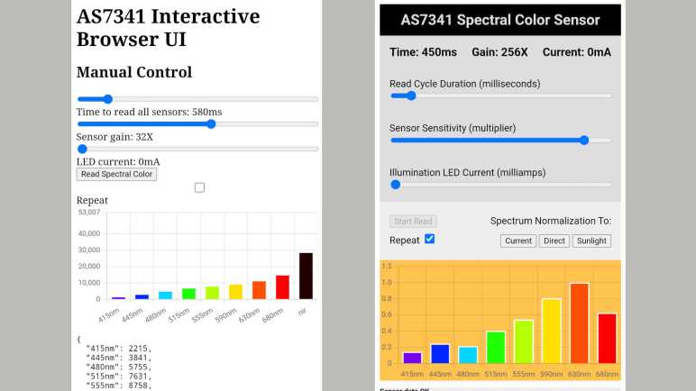
This was my first opportunity to apply what I learned from Codecademy outside of their CSS course exercises, though I did make this project easier for myself with a few design decisions. I didn’t need to drastically change the layout, HTML’s default top-to-bottom arrangement would suit me just fine. I’m only dealing with a single page, so there’s no concern of site navigation controls. And finally, I decided not to worry overly much about creating separate mobile vs. desktop layouts: everybody gets the same thing. No media queries in my stylesheet. I intended to use this web app on my phone, so I want it to look good in portrait mode. On my desktop, I can easily resize my browser window to match the aspect ratio of phone in portrait mode. The minimalist nature of this app meant there were no additional data I could add to a desktop view anyway.

Hit target size was a concern. Parameter sliders were fine, but I was worried about the buttons selecting normalization curve. Fortunately there were no problems in practice. However, I had some trouble with my “repeat read” checkbox being too close to the “Start read” button, and I think I will eventually need to space them further apart.

This was a good start. A few lines of CSS made the page look much more pleasant to my eye. Enough that I can go back and add a few more bits of nice-to-have functionality.


Code for this project is publicly available on GitHub

AS7341 Sees Sunlight Very Differently From LED

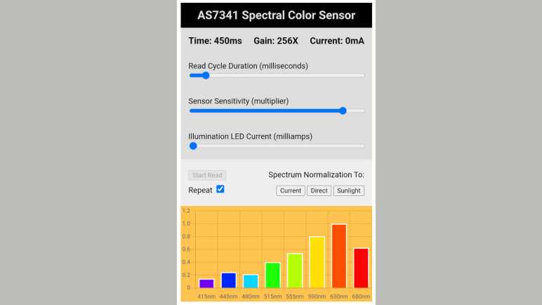
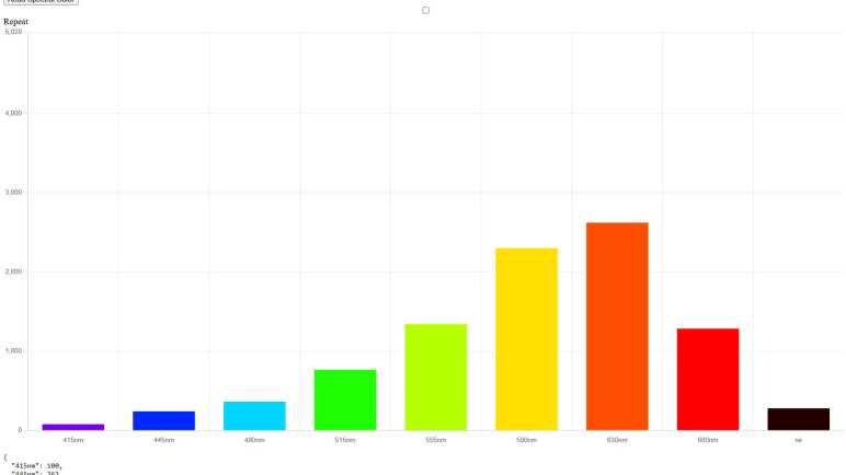
Thanks to Chart.js documentation, I was quickly up and running with a simple bar chart to visualize AS7341 data. My first draft was done late at night, so this chart corresponded to the spectral distribution of my room’s ceiling light.

With an advertised color temperature of 2700K, its “warm white” showed a strong response in the yellow and orange areas of the spectrum. The next morning, I had a ray of sunshine coming in a window and I set my AS7341 sensor within it.

The first lesson was that sunlight — even just a tiny beam at an oblique angle — is significantly stronger than my ceiling light. Direct exposure will always reach sensor saturation (ADCfullscale value) no matter what I do. I ended up placing a sheet of printer paper at my sunlight spot and aiming the sensor at that reflected light.

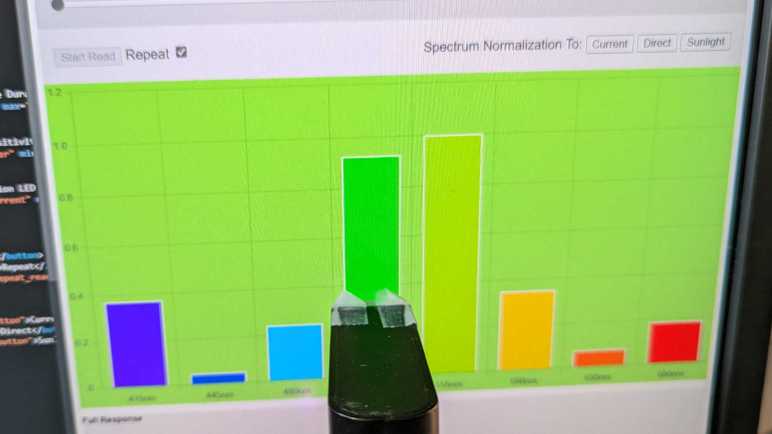
This spectrum has whatever distortion added by a sheet of paper, but it is still very interestingly different from my ceiling light. There is a huge response on NIR sensor, and there isn’t as strong of a peak on orange. My brain sees both of these light sources as white, but the sensor sees very different spectrum between them. Raw sensor data (with clear channel hitting saturation) are as follows:

{
  "415nm": 5749,
  "445nm": 6342,
  "480nm": 9533,
  "515nm": 10746,
  "555nm": 11245,
  "590nm": 12577,
  "630nm": 12633,
  "680nm": 15217,
  "clear": 65535,
  "nir": 34114,
  "settings": {
    "atime": 30,
    "astep": 3596,
    "gain": 64,
    "led_ma": 0,
    "read_time": 674
  }
}

According to AMS AS7341 calibration application note, knowing NIR level is important for properly compensating values of spectral sensors F1-F8. They are sensitive to whatever NIR leaked past their filters, so knowing NIR level is important for precise color accuracy. The clear channel and flicker channels likewise have their own impact on color accuracy. But since I’m just goofing around and not concerned with utmost accuracy, I’m choosing to ignore them and dropping NIR from my visualization.

I will, however, make use of this sunlight spectrum to compensate for the differing sensitivities across spectral sensors F1-F8. Using sunlight as my reference for a light source emitting all wavelengths of light, we confirm AMS AS7341 datasheet information that 415nm is the least sensitive and 680nm is the most sensitive. I can selectively boost sensor values so that F1-F8 would all return the same value under direct sunlight. This is crudely analogous to a camera’s color balance (or “white balance”) features, and I implemented the following normalization options in my app:

  • Default normalization curve based on these sunlight values.
  • A direct data option skipping the selective boost.
  • An option to use the next sensor reading as reference. I can point the sensor at something and activate this option to tell my app: “treat this color as white”.

Each of these options had a corresponding button onscreen. Functional, but the jumble of controls on screen is starting to cause usability problems. I built this app and if I get disoriented, how bad would it be for everyone else? It’s time to put some effort into layout with CSS.


Code for this project is publicly available on GitHub

Chart.js For Visualizing AS7341 Data

There’s no shortage of web frameworks that help us put pretty things on screen. I’ve been eyeing A-Frame, Three.js, and D3.js for use in the right project but all would be overkill for my AS7341 interface: I just need to plot eight data points and there’s no need for interactive drill-down. Would the web development ecosystem have something that fits the bill? The answer is definitely “Yes” because this is the same ecosystem that gave us “leftpad” and the debacle it caused. Yeah, I could spend a few hours and write my own, but I know I don’t have to.

I went on NPM to search for charting modules and as soon as I typed “chart” I got the suggestion to look at Chart.js. A brief read of documentation told me this fits my needs. Simple, lightweight, and minimal interactivity capabilities that I plan to turn off anyway. No need for fancy graphics of WebGL or DOM interactivity of SVG, Chart.js draws onscreen using HTML Canvas. Canvas was the API I used for my Micro Sawppy browser interface, so I have a rough idea of what Canvas could and could not do.

With my limited needs, I don’t expect to use most of Chart.js capabilities. But I’m happy to incorporate those that are convenient and require minimal/no effort on my part. One good bit of visual polish is its ability to animate updates to chart data, smoothly growing or shrinking bars in my bar chart based on updated AS7341 sensor data. Another bit of convenience was the ability to specify color used for each bar. I could draw the bar for one AS7341 sensor with the color that corresponds to its wavelength, which helps give me an intuitive grasp of the spectrum seen by AS7341. A quick web search found Academo’s interactive wavelength to color converter and I used that to determine colors of each bar F1-F8.

What about the other sensors? I’m completely ignoring the flicker detector right now, and I decided not to draw the clear channel. From my experiments, the clear channel typically has the highest value (which makes sense as it’s the sensor without any color filters blocking input) so I used its value as the Y-axis maximum. I also plotted the near infrared channel, but since it’s invisible I plotted it using an arbitrary chosen dark red color. This seemed to work when I first wrote the code late at night under artificial light. The next morning, I played under natural sunlight and that was an entirely different beast.


Code for this project is publicly available on GitHub

Overkill Options: A-Frame, Three.js and D3.js

After getting input controls sorted out on my AS7341 interface project, it’s time for the fun part: visualizing the output! Over the past few years of reading about web technologies online, I’ve collected a list of things I wanted to play with. My AS7341 project is not the right fit for these tools, so this list awaits a project with the right fit.

At this point I’ve taken most of Codecademy’s current roster of courses under their HTML/CSS umbrella. One of the exceptions is “Learn A-Frame (VR)“. I’m intrigued by the possibilities of VR but putting that in a browser definitely feels like something ahead of its time. “VR in a browser” has been ahead of its time since 1997’s VRML, and people have kept working to make it happen ever since. A brief look at A-Frame documentation made my head spin: I need to get more proficient with web technologies and have a suitable project before I dive in.

If I have a project idea that doesn’t involve full-blown VR immersion (AS7341 project does not) but could use 3D graphics capability (still does not) I can still access 3D graphics hardware from the browser via WebGL. Which by now is widely supported across browsers. In the likely case working directly with WebGL API is too nuts-and-bolts for my taste, there are multiple frameworks that help take care of low-level details. One of them is Three.js, which was the foundation for a lot of cool-looking work. In fact, A-Frame is built on top of Three.js. I’ve dipped my toes in Three.js when I used it to build my RGB332 color picker.

Dropping a dimension to land of 2D, several projects I’ve admired were built using D3.js. This framework for building “Data-Driven Documents” seems like a great way to interactively explore and drill into sets of data. On a similar front, I’ve also learned of Tableau which is commercial software covering many scenarios for data visualization and exploration. I find D3.js more interesting for two reasons. First, I like the idea of building a custom-tailored solution. And second, Tableau was acquired by Salesforce in 2019. Historically speaking, acquisitions don’t end well for hobbyists on a limited budget.

All of the above frameworks are overkill for what I need right now for an AS7341 project: there are only a maximum of 11 different sensor channels. (Spectral F1-F8 + Clear + Near IR + Flicker.) And I’m focusing on just the color spectra F1-F8. A simple bar chart of eight bars would suffice here, so I went looking for something simpler and found Chart.js.

AS7341 ADC Fullscale and LED Illumination Control

Getting interactive control over AS7341 sensor parameters helped me better understand their effect on resulting data. Interactive control over sensor integration time (photography analogy: exposure time) made it easy for me to see how the data reacted mostly linearly until they reach their limit. I had known the AS7341 ADCs were 16-bit, so I thought the limit is always 65535. This is wrong: it is actually 65535 OR ADCfullscale, whichever is lower.

I came across ADCfullscale in the datasheet but I didn’t understand what that information meant at the time. I had mistakenly thought it placed a limit on integration time, as it is calculated from integration time parameters “atime” and “astep” with the formula (atime+1)*(astep+1). Now I know it does not limit integration time but is actually a cap on ADC values if that formula results in less than 65535. For example, right now I’m running with a fixed “astep” of 3596 which corresponded roughly to 10 milliseconds per “atime”. If I configure “atime” to 9, (atime+1)*(astep+1) = (10)*(3597) = 35970 is the sensor saturation limit ADCfullscale. Not 65535.

Another thing I learned was that my original plan for “LED stay on” parameter wouldn’t work. I had designed it to be a parameter sent alongside atime, astep, and gain at the beginning of sensor read. It seemed reasonable enough until I tried to design a control to toggle whether we are going to read the sensor continuously. When will the user toggle that to be “OFF”? Odds are, such toggle would happen while we are in the middle of sensor integration. By that time, it was too late to communicate LED should be turned off.

Oh well, mistakes like this happen. That useless “led_stay_on” parameter was removed, and I added code so “led_ma” could be a valid operation by itself without triggering a sensor read. This lets me adjust the LED illumination (usually turning it off) without performing a sensor read. Just another instance where iterative development is useful, updating my design as I go.


Code for this project is publicly available on GitHub

Notes on AS7341 Integration Time

After pleasantly surprised at the fact my web app project is unlikely to leave my old Android phones behind, I got back to my “learn by doing” process. As originally planned, I’m going to leave my first draft “Basic” UI as-is for fallback/debug purposes. I made a copy to serve as the starting point of my “Standard” UI and initial focus is on sensor integration time.

Full Width Control

First change was minor and cosmetic: “Basic” didn’t use any CSS styles, and “Standard” started with just one style to make input sliders 100% of available width. The default width was annoyingly narrow. Making it full width helps me make finer adjustments.

ASTEP Value Fixed at ~10ms

AS7341 sensor integration time is controlled by two parameters: ATIME and ASTEP. As per datasheet, the resulting integration time follows the formula: (ATIME+1)*(ASTEP+1)*2.78 microseconds. My “Basic” UI exposed both parameters directly, but I want to use something more human-friendly for the “Standard” UI. I decided to keep ASTEP fixed at 3596. Per the formula (3596+1)2.78 microseconds = 9999.66 microseconds, or just a tiny bit less than 10 milliseconds. Keeping ASTEP fixed at 3596 means the ATIME range of 0-255 can dictate integration time anywhere from 10ms to 2560ms a.k.a. 2.56 seconds. This covers the entire time range I want for initial experiments. I may adjust this range in the future after playing with the sensor some more.

Read Time is Double Integration Time

Once I had set up the UI to adjust integration in 10ms increments, I took a few readings at various settings and noticed the actual time spent in readAllChannels() is a lot longer than integration time. If I configure for 1 second (1000ms), I end up waiting two seconds. I added a bit of tracking code to my ESP32 Arduino sketch and verified it wasn’t just my imagination: actual read time is over double integration time.

This was puzzling until I remembered readAllChannels() implementation: it configures AS7341 sensor multiplexor (SMUX) to read sensors F1-F4 plus clear and NIR, performs a read, then configures SMUX for sensors F5-F8 (keeping clear and NIR) and perform a second read. So, a one-second sensor integration time meant one second spent for F1-F4 and another second spent on F4-F8. Add in a few tens of milliseconds for processing and communication overhead, and we’ve explained the observation of a little bit over twice integration time.

This is something to keep in mind depending on sensor application. For example, if I want my browser UI to update once a second, I need to set integration time to be less than half a second.

UX Design Decision

Which led to the next question: Should my browser UI show the integration time, because that’s how I’m configuring the sensor? Or should it show double that time, because that is a better estimate of time I should expect to wait for a reading? I decided to go with double for my “Standard” UI: this is a user experience issue, so I should be faithful to what the user will experience.


Code for this project is publicly available on GitHub

Impressively Long Tail of Android Chrome Updates

I had hoped writing browser-based apps would let me put old phones to productive use, but the effort-to-reward ratio is really bad for my old Windows Phone 8.1 devices. After a short investigation, I will treat WP8.1 as a separate platform with their own (TBD) project focused just on the capability they have. I’m not going to worry about that platform for general-use browser apps like my AS7341 web app. Does this decision also rule out Android phones of similar vintage? I was surprised to learn the answer is “Not Really.” It appears Google keeps Chrome updated for Android phones well after they stopped receiving Android updates.

My data point for this investigation was my Nexus 5 phone, which was my personal successor to my Lumia 920 Windows Phone. The hardware is old enough its battery degraded enough to start puffing up. That was replaced with a buck converter pretending to be its battery so I could continue using the device. I powered it up to answer the question: how out-of-date is the Chrome browser on this thing? After updating everything available from Google Play store, I tapped on “About Chrome” and was amazed to see version 106.0.5249.126 which was released October 13th 2022.

For context, Nexus 5 launched in 2013 with Android 4. It received next two major Android updates and now runs Android 6, which stopped receiving updates in 2017. Due to this fact I had expected Chrome version to date back to a similar timeframe. Contrary to my expectations, Google continued to update Chrome for Android 6 even though the operating system itself stopped receiving updates, continuing five more years all the way to late 2022. But Chrome 106 was the end of the line, my Nexus 5 could not pick up 107.0.5304.54 released a week and a half later on October 25th, 2022. (Annoyingly, this meant Chrome 106 would display a “Chrome update now available!” prompt even though this phone can’t get Chrome 107.)

Looking around for a definitive resource on Chrome support, I found the “Chrome browser system requirements” page. Today it says the minimum Android version is Android 7, which is consistent with my Android 6 phone being left out. Android 7 received its final system update October 2019 yet is still receiving updates to its Chrome browser. This story of Chrome updates far surpassed my expectations and puts my Nexus 5 phone in a far better position than my Lumia 920 phone. Having a 2022-era browser should mean it can run my AS7341 interactive web app with no special treatment at all.


Unknown: Does Apple continue to update Safari for old iOS devices even if they have stopped receiving iOS updates? In a quick web search, I found no information one way or another and I do not have an end-of-life iOS device to check Safari version numbers firsthand.

Windows Phone 8.1 Browser Effectively a Separate Platform Now

For the first draft of my latest browser app, I aimed to write simple JavaScript. Since I didn’t use any feature I considered “fancy” I had expected it to work on older browsers as well. This proved to be false for Windows Phone 8.1 browser. Microsoft took down Windows Phone developer resources years ago, but I could see what went wrong by using developer console of Internet Explorer 11 (close relative of WP8.1 browser) on a Windows desktop. It confirmed what I had suspected: web development state of the art has advanced far enough that it would take a tremendous amount of effort to maintain compatibility with WP8.1 browser/IE11.

When it was new, WP8.1 browser support for mobile-focused websites were pretty good. This was somewhat out of necessity: mobile developers tend to release dedicated iOS and Android apps, leaving WP users to their website, so the browser had to work. Roughly on par with competitors of its day, mobile site authors could support WP8.1 with minimal (or no) additional effort. But the web moved on and WP8.1 did not. Soon support for such browsers became an explicit opt-in that fewer and fewer people chose. With support dropping left and right, Microsoft will soon forcibly remove IE11 from existing installations of Windows.

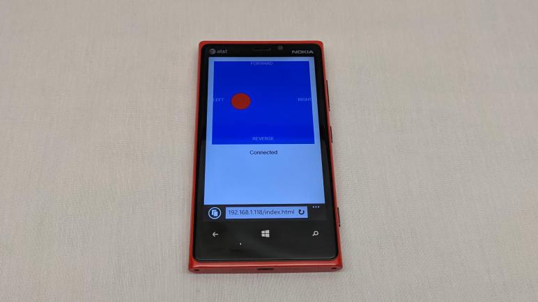
It hasn’t been practical for several years to “just” keep a browser app project compatible with IE11/WP8.1. Even worse now that IE11 debugging resources are being removed. I still hold hope of using my old Windows Phones in a project of some sort, but it would have to be a dedicated project focused on using just the capabilities it has. It has become effectively a development platform separate from modern web development. Based on my earlier ESP32 Sawppy controller project, I know I still have access to the following: draw to screen with HTML Canvas, touch input with PointerEvent, and communication with WebSocket. This is a tiny subset of the breadth of modern web development, but enough foundation to build something neat. I have to think up a project idea and do it before all IE11-related debugging resources disappear.

In the meantime, I’m going to ignore WP8.1/IE11 compatibility for my AS7341 interactive web app. I will move forward with an improved user interface and only have to worry about how it works on my Android phone Chrome browser.