As a learning exercise, I decided to generate my own documentation for commodity L298N motor driver modules available wherever hobbyist electronics are sold. The first step was to catalogue all the components mounted on board, and now I analyze the circuit board layout to see how they are connected together. And as much as I like to do things digitally, for projects like this I really appreciate the flexibility and immediacy of a sheet of paper to scribble on.

I could probably do it with the actual device in hand and a blank sheet of paper, but this time around I decided to create my own visual guide. I took photos that are as directly square-on as I could front and back. I scaled them to the same size, and printed them side by side on a sheet of paper leaving room for me to write notes. Once printed, I folded the paper in half while holding it up to a light source so I could line up the front and the back. Then I started following copper traces and scribbling my notes.
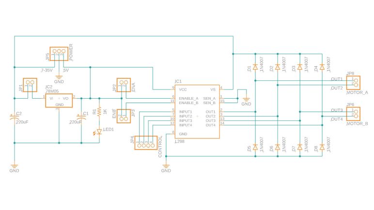
Fortunately this was a relatively simple circuit that mostly followed data sheet recommendations. I quickly confirmed the eight diodes were present to dump excess power into the +12V and GND planes. The two electrolytic capacitors are there for the +12V and +5V power planes respectively. IN1 through IN4 and OUT1 through OUT4 are straightforward direct routes. I also confirmed the optional current sensing resistors were absent, those pins were tied directly to ground. Furthermore, there was no provision to make adding current sensing resistors easy. People who want to perform current sensing are probably better off using another module.
A few traces were buried under components so their paths had to be teased out via probing with a continuity meter. The jumpers on ENA and ENB do indeed tie them high to the +5V power plane. The third jumper enable/disable the onboard 78M05 regulator. When the jumper is in place, it connects the +12V power plane to the input pin of 78M05. Which can then supply 500mA of current to +5V plane. Since the L298 itself draws less than 100mA, the remainder capacity can be tapped via the +5V screw terminal to perhaps drive a microcontroller. When the jumper is removed, regulator input is disconnected from the +12V plane and the +5V screw terminal becomes an input port to accept external power. The LED and current-limiting resistor is connected to the +5V plane and will illuminate when +5V power is present.
Aside from the silkscreened text proclaiming +12V, I found nothing to limit motor power supply to +12V. As far as I can tell it can be anywhere from 7 to 35V when using the onboard 78M05 regulator. If the regulator jumper is removed and L298N is running on external logic power, the lower limit is dictated by the L298N which can function with as low as 4V. The upper limit of a L298N is 45V with peaks of 50V, but the capacitors and 78M05 used on this module are listed with 35V maximums. Personally I’m unlikely to use anything higher than two 12V lead-acid batteries in series, which would be 28.8V fully charged and comfortably under that limit.
As a part of this self-assigned exercise, I also practiced drawing a schematic using the electronics design component of Autodesk Fusion 360. I think I’ve captured all of the information above, though I’m sure this schematic violates a bunch of conventions and make electronic engineer eyes twitch. (I’ve had to read software code written by electrical engineers so I have some idea what the mirror image is like.) And while I try to put lots of comments into my software source code, I haven’t learned how to best document a schematic. Until I learn more about that world, this blog post represents my best effort for this round.
Armed with this knowledge, I felt confident enough to embark on designing a micro rover to use TT gearbox with its DC motor, leading to Micro Sawppy Beta 3.

thank you so much! that was very helpful for me. greetings from Brazil
LikeLike
Can I use your schematic image in our website with credit and a link to your site? Than you.
LikeLike
What’s your website?
LikeLike
https://dcc-ex.com Model Railroading using Arduino and other microcontrollers and motor drivers
LikeLike
Specifically this page: https://dcc-ex.com/reference/hardware/motorboards/L298N-motor-board-setup.html. Thank you!
LikeLike
That looks like a great community support resource, I would gladly contribute my schematic. Please feel free to use my image with link back to my site, thanks!
LikeLike
Nice diagram. You can compare your schematic to the one provided in the typical documentation for this device: https://www.handsontec.com/dataspecs/module/L298N%20Motor%20Driver.pdf. Apart from being laid out in a manner that makes it very difficult to follow because it relies on labels rather than direct connects, it fails to explain what J5 and J7 are (they are the other half of the Enable jumpers) and shows only 1 of the sense inputs grounded. The layout makes it particularly difficult to figure out how the 5V input select jumper works – quite a problem considering that incorrect usage of that jumper could destroy the device. Schematics don’t usually include much text description, because the presentation should make the function clear. Many current examples simply don’t do that.
LikeLike
Very useful diagram. It is surprising that they didn’t add the few cheap components for short circuit protection as described in an SGS-Thomson application note. That addition reacts to a short to ground in 10usecs – using a 10K0 resistor, 1N4148 fast diode, 1.5nf capacitor. SGS-Thomson apparently published it in 1995 – together with other useful application data for the L293 and L298.
Click to access an240-applications-of-monolithic-bridge-drivers-stmicroelectronics.pdf
LikeLike
That application note is a good find, thanks for the link. Perhaps whoever originally designed this board followed just the datasheet and didn’t know about the application note.
LikeLike
Because many circuits would not work with such a short “short” detection time 😉 We’ve taken to calling it OCP for “overcurrent protection” and it is the bane of our existence. In our applications, there is capacitance at the output. That capacitance has a large inrush current that can last up to 100ms, we can’t have the chips cutting out, or cutting out then trying again and the capacitance hasn’t been charged so it tries again, etc. This is an issue with many other new motor drivers.
The L298 is ancient technology powered by bipolar output transistors. It can’t do more than about 1.3A with that heat sink and with a fan in a cold room. Not only that, but the voltage drop is SIGNIFICANT and not steady, it rises with the current so it not predictable. The chip passes spec if up to 3.9V is dropped at the output! At least it doesn’t cut out in 6uS 😉
And the last thing is we need current sensing and for whatever reason, this board chose to put both CS pins to ground rendering them useless (at least the Arduino Motor Shield uses current sensing). We tell our users to lift the CS legs or cut traces on the bottom an insert current sense resistors.
I know it has it’s uses, like if you just need a cheap 1A or under board for 1 or 2 motors, but we use MOSFET based motor drivers pretty exclusively, either discrete or fancy chips like the DRV8874. We have tried almost every motor driver in our development testing.
For people using an L298, we sense the current and shut it down in software, but it does throttle itself if it overheats.
Many people are using the IBT_2 motor driver board that is similar to this one but can handle a significant amount of Amps. The MOSFETS have a very low RDSon, so can handle 8-10 with no cooling. The only issue with these for us is that each BTS7960 chip differs wildly in its current sense output, and with 2 on that board, you have to usually join both CS pins together and then calibrate to what it outputs and then protect against the CS output going over the voltage on the pin in a microcontroller you are using to read it. We finally designed our own motor shield that fits our unusual use for controlling model trains and now can’t make them fast enough 😉
Thanks again for taking the time to write this article, Roger. It’s fun to tinker!
LikeLike
Thanks for that Fred. It is a 12vdc model train layout – so track shorts are inevitable.
The current track points/turnouts have microswitches. The layout redesign was to automatically identify the resultant live track sections instead. When the controller voltage is OFF – a “standby” low voltage (2v) was to be injected into the track to maintain the configuration information. Such a supply should be resilient to transient or fault current overloads. However – I feared that even a small constant voltage would potentially overheat some of my modern expensive locomotives in their stall mode.
Experimenting with >20kHz PWM with a low duty cycle as the tracer current. The sensor hardware and software works nicely as proof of concept. Hopefully it would not be enough power to move a locomotive – but stall current might trigger a sensitive protection mechanism even at 2v.
Have played with some of the MOS H-bridges – but they seem to need at least a 10v supply – which is overkill for a 2v end result.
DCC is not an option as there would be over 100 to retrofit.
It’s just my neighbourhood contribution as an Advent Calendar for the passing school run. Keeps my brain active and my fingers nimble.
LikeLike