Roku Premiere (4620X “Cooper”) Circuit Board

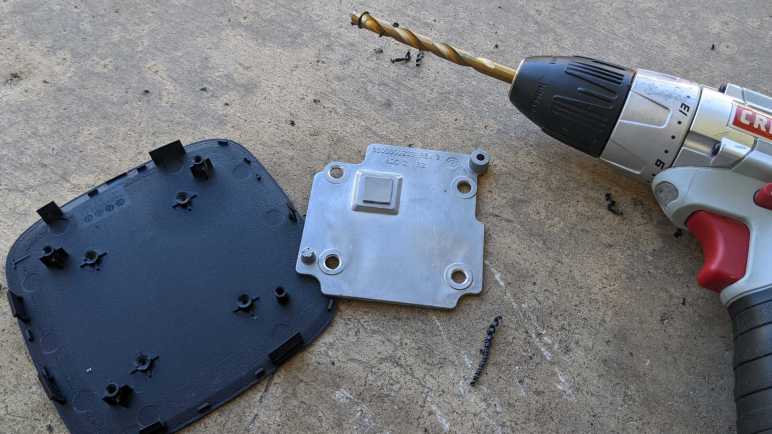
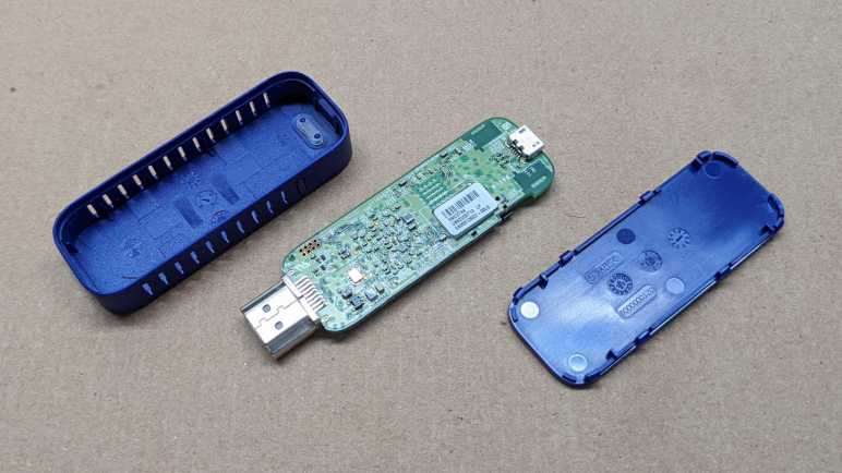
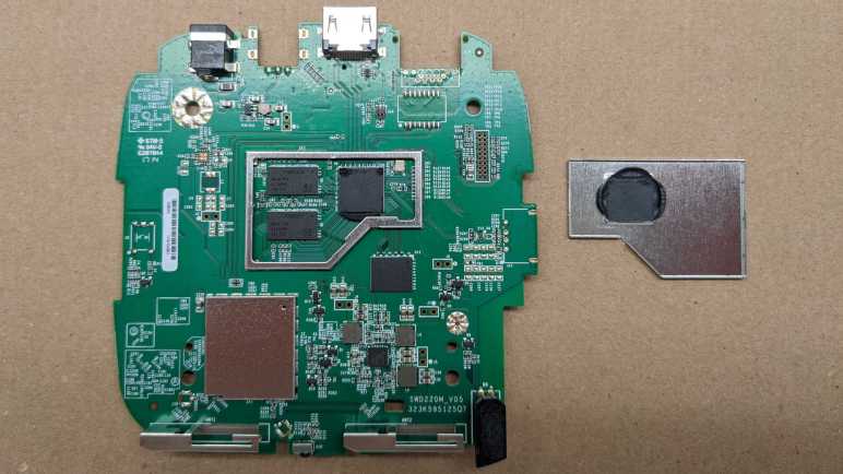
After examining the enclosure of a Roku Premiere model 4620X (“Cooper”) that I took apart, attention turns to the solitary circuit board inside the device. A piece of cast aluminum under its top lid has all the appearance of a heat sink, so the first thing I did was to pop off the thin metal shield to confirm – yep, there’s a microprocessor under there. With a bit of black thermal compound to bridge the small gap between it and the metal shield.

The other metal shield is directly soldered to the board and I couldn’t remove it (nicely) to see what’s inside. So I flipped the board over instead. I see a shield whose shape mirrored the top shield and covers nearly (if not exactly) the same area.

In comparison to its topside counterpart, it has an extra twist in the form of extra metal bridging the center in a “T” pattern. Or maybe a circle with three legs? This must be intentional, but I couldn’t figure out why.

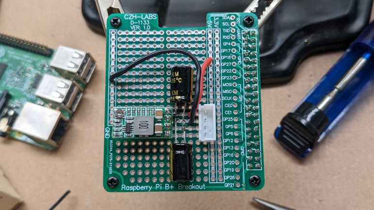
And just for fun, here is the board side-by-side with a Raspberry Pi 4, which has broadly similar specifications of an ARM-powered 4K UHD capable networked device.

Using a cotton swab and some isopropyl alcohol, I cleaned off the thermal compound to read markings on the CPU.

I see two logos: a stylized “M” (MediaTek?) with ARM, and below them the following:

MS09380AMZ-R62-NA1
ATKR524B
1637B

Several connectors are visible around the board, not all of which are used. Starting from the upper left, we have the power connector.

There are five soldered points, but all four along the sides are electrically connected to ground. Only the bottom center point is different, picking up 12V from the AC adapter. Below it is a large round contact point (with a bit of solder) is one of two grounding points for the aluminum heat sink.

To the right is an unpopulated connector also with four surrounding ground points but with three unused electrical contacts. I’m not sure what this would be. My first thought was maybe an alternate video connector, but there aren’t enough pins to be any type of DisplayPort. Composite video or S-Video are too old-school for this 4K-capable video streaming box, so I ruled those out. It is too small to be a pair of RCA jacks for analog audio, so my best guess is a provision for TOSLINK audio.

Next is the HDMI connector, with several meticulously routed differential signal pairs visible.

The final connector on this edge is probably an 8P8C connector for wired Ethernet, with an adjacent unpopulated chip footprint that’s likely to relate to wired networking. Their absence means this particular Roku is WiFi-only.

On the left edge of the board is definitely a switch, electronic schematic symbol for switch and everything. Since there’s already a reset switch on board, this is probably used for a development/test/debug purpose.

On the right edge looks like provision for a USB type-A socket. It may be for similar dev/test/debug purposes, but Roku may have also contemplated the option of a USB port so it can play a slide show of pictures on a USB flash drive. This is a feature I see on many other media boxes.

The bottom of the edge has two antennae, and my RF skills aren’t enough to know what to do with them. A status LED is on the right edge, but I have plenty of LEDs and saw nothing particular special about this one. In between the antennae, though, is a receiver for the infrared remote. I’ve come across similar receivers before, and I always thought “that might be fun to play with” but never did… until now.

Roku Premiere (4620X “Cooper”) Enclosure

I’ve just disassembled a retired Roku Premiere model 4620X, also named “Cooper”. I had expected its enclosure to be just a plastic box, but it turned out to have a few points of interest. The most unexpected item was the Roku fabric tag sticking out the side.

It was clearly a piece of branding, and I thought it was pretty clever how Roku could do that by sandwiching a little piece of fabric into the seam of their enclosure. That would be super simple and inexpensive to manufacture. But then I realized… there’s no seam here! The fabric tag is actually coming out of a dedicated slot in the side of the case. This slot, which is perpendicular to the motion of their plastic injection mold, would have added cost to the process.

And since it’s not sandwiched in an existing seam, it’s not held in place by an existing fastener either. This is a separate piece (or multiple pieces?) of plastic dedicated to a Roku name tag, adding to parts cost and assembly complexity. I thought the Roku fabric tag was a cheap thing to throw in there, but no. This required a very deliberate decision in product design. A little web research found that this is actually a registered Roku trademark. I had originally dismissed it as unimportant, I guess this is why I’m not a hotshot product designer.

A metal plate stamped with “6000000235 A1 REV2” is at the bottom. A small cutout on one edge gives extra clearance for the reset button, and four plastic posts help support the main circuit board. The plate itself was fastened to the plastic enclosure by four blobs of melted plastic.

The four blobs of melted plastic were quickly dispatched with a drill, freeing the plate. There was nothing remarkable on the other side. It seemed to have been stamped out of sheet metal. It is not magnetic, so I am going to guess aluminum. At a weight of roughly 10 grams (about one third of an ounce) it is too light to serve as unnecessary weight designers sometimes add to products for the sake of a “premium feel” heft. It does add a bit of support to the structure, but the enclosure did not feel noticeably flimsier with its removal. Perhaps it adds strength along an axis I didn’t test? There is no mechanical contact with the circuit board, so it is not a heat sink. There are no electrical contacts with the circuit board, either, so it is not an antenna. But it might be an anti-antenna serving as RF shielding. Though RF shields usually have a connection to electrical ground on the circuit, which it lacks. What is the purpose of this metal plate? I’m stumped.

The top plate, in contrast, has an obvious purpose as heat sink for the processor. Its shape hints at a casting process, and it is also nonmagnetic so I’m going to guess aluminum here as well. Imprinted from the casting mold are the markings “6000000233 REV 3 ADC 12 B2” and a circular indicator with seven out of twelve positions filled with a dot and “16” in the center. It probably means something to the people running the manufacturing process but not tome.

I usually see heatsinks from the desktop computer world, where they are precision ground to tight tolerances for optimal contact with the processor. This piece looks to have received no post-processing machining after being cast. Instead, a square of squishy thermal pad takes care of filling the ~1mm gap. It would be less thermally conductive than what is used for desktop processors, but probably just fine in this context. Aside from the raised square section to make contact with the processor, there are two circular posts (upper right and lower left in picture) to electrically ground this piece of metal.

A quick visit by the drill freed this plate as well, and this time its structural support was more noticeable. The lid was pretty flexible once it was removed. It is also a beefier piece of metal at 38g, almost quadruple the weight of bottom plate but still not exactly “heavy”. I doubt the weight is the point of the exercise, so the most likely primary purpose is heat sink for the circuit board.

Roku Premiere (4620X “Cooper”) Teardown

I’ve been gifted two retired Roku devices for teardown. The small streaming stick was straightforward, now it’s time for the far more interesting Roku Premiere. I also have its AC power supply and remote control.

Looking up the model number 4620X listed on the bottom of the case, we find these specifications on Roku’s hardware reference chart:

Device NameRoku Premiere
Code NameCooper
roDeviceInfo.GetModel()4620X
CPUARM Cortex A53 quad core 1.2 GHz
RAM1 GB
Accelerated Graphics APIOpenGL ES 2.0
Max UI Resolution1920X1080
Max Playback Resolution4K UHD, 60fps
HDR Supportn/a
IDK SupportNo

Whereas the streaming stick was roughly analogous to a Raspberry Pi Zero, the 4K UHD capabilities here put this item closer to a Raspberry Pi 4. A more capable piece of hardware that is fed more electrical power as well. Its power supply (model PA-1120-42RU) is specified to deliver 12 volts DC at up to 1 amp.

Unlike a streaming stick, a Premiere can be set in line of sight of the user so its remote control (model RC108) is infrared. I plan to play with this later.

I see a seam around the top of this enclosure, and a bit of prying could release some plastic clips. But they would immediately snap back. I suspect some fasteners are hidden under the bottom, which is a soft rubbery surface that gives the device good traction to resist sliding around.

I had expected annoying strong glue to hold this in place, but it actually peeled off easily. Not as easily as normal cellophane (“Scotch”) tape, more like packing tape or duct tape.

I see my primary target: four Philips-head screws. I also see the reset button through a window in the case, a hard nub on the rubber base helps us push it when needed. Towards the upper left of this picture, we can see another window exposing test and/or debug points.

Those four Philips-head screws were revealed to be self-tapping plastic screws upon removal. Then I resumed working on the lid, and this time its clips could be freed and stay freed.

Once clips were freed, the lid could be removed exposing a circuit board.

There is only one layer to the circuitry, below that is the bottom of the case.

Here are the components laid out.

There were a few features that caught my interest that’s worth a closer look, starting with its external enclosure.

Roku Streaming Stick (3500X “Sugarland”) Teardown

A friend gave me this retired Roku streaming stick to take apart. Before I did, I looked to see if I could do something fun in the software realm and found the Roku IDK. Sadly this device lacks IDK support so it is getting taken apart.

A streaming stick is pretty simple piece of hardware. The device itself has two connections: an HDMI plug to go into your TV, and a micro-USB port for power. A reset button is the lone user input, and a LED the lone user output. The power supply looks like a standard AC powered USB power supply advertised to deliver up to 1A at 5V, but it has Roku branding which is more than what some other devices ship with. This device should also have a radio frequency (RF) remote control instead of the usual infrared, since infrared requires line-of-sight and that won’t work for a streaming stick behind the TV. But I was not given the remote, or I have lost it.

On the back I see a model number of 3500X. Roku’s hardware reference chart lists the following information for 3500X:

Device NameRoku Streaming Stick
Code NameSugarland
roDeviceInfo.GetModel()3500X
CPUARM11 600 MHz
RAM512 MB
Accelerated Graphics APIOpenGL ES 2.0
Max UI Resolution1280X720
Max Playback Resolution1280X720
HDR Supportn/a
IDK SupportNo

Based on these specifications, the hardware within is less powerful than a Raspberry Pi Zero. The latter has a CPU running at a higher speed, double the RAM, and could output 1080p resolution UI. However, video playback on the Pi is not its greatest suit. In contrast, video playback is a Roku’s main purpose, so I assume it has access to video acceleration that Broadcom has limited access to Pi.

Using an iFixit opening tool, I pried against a visible seam on the back and quickly unsnapped six clips holding the enclosure together. The circuit board was removed without fuss.

There’s not a whole lot to see on the back. There is a large IC under the sticker, and an array of test points in the upper left. Probably a debug header for the onboard processor, but that’s beyond my hardware skill today.

A thin metal shield covers most of the front side. Visibly outside the shield is the LED, the reset button, and antenna 1 and 2. Once the thin metal shield was removed, we could see the main processor with the following markings:

Broadcom
BCM43236BKMLG
HE1537 P21
5383606 3 W

To its right are two smaller chips, and to its left, a chip by Samsung whose markings were tall and narrow and very difficult to read.

Here is a Raspberry Pi Zero WH (Wireless Header) next to the streaming stick, a fun comparison as these two share some similarities in functionality. Even if this Roku streaming stick supported their IDK, for projects that do not involve video playback I would probably choose to use a Raspberry Pi instead. Since IDK is not supported, this circuit board is going to electronic waste. This was a quick teardown, as appetizer for the more interesting Roku Premiere teardown.

Window Shopping Roku IDK (Independent Developer Kit)

I’ve been given a pair of Roku streaming devices that were retired from a friend’s household, as they knew I like to take things apart to look inside. Before I do that, though, I briefly investigated what might be fun to do with intact and functional Roku devices. I was quite pleasantly surprised to learn that Roku has recently (announcement dated October 26th, 2021) released an Independent Developer Kit (IDK) for hobbyists to play with Roku hardware. This is different from their official Software Development Kit (SDK), which is available to companies like Netflix to create their Roku apps (“channels”). Many other differences between the IDK and SDK are explained in their IDK FAQ.

The Roku SDK requires a business partnership with Roku, but the IDK is available to anyone who is willing to work at low level in C++ and has a Linux development machine available to the task. No direct support for Windows or MacOS, but as the resulting binary is uploaded through a web interface, theoretically a Linux virtual machine could be used to run these tools. The list of example apps hint at what is accessible through the IDK: the OpenGL ES API, interface to the Roku remote control, interface for audio playback, and interface for video playback. (Including Wildvine DRM-protected content.) And it sounds like an IDK app has pretty complete control of the machine, as only one IDK can be installed at any given time. If it takes over the Roku shell, that implies control over the entire system even greater than possible with SDK-developed Roku channels.

But I couldn’t test that hypothesis due to the final requirement: a Roku device with IDK support. A chart listing all Roku hardware has a row for “IDK Support” and the old devices I’ve been gifted are both shown as “No”. If I really want to play with the Roku IDK, I’d have to go out and buy my own Roku device with a “Yes” listed on that chart. At the moment I don’t see the advantage of buying Roku hardware for this purpose. On the surface Roku IDK appears less compelling than developer support available on Google Chromecast or Amazon Fire TV devices. Or for ultimate openness, we can go with a Raspberry Pi. Maybe I’ll find a reason for Roku projects in the future, in the meantime these two old devices without IDK support will be disassembled. Starting with the smaller streaming stick.

Recording ESPHome Sensor Values: Min, Max, and Average

I’m learning more and more about ESPHome and Home Assistant, most recently I was happy to confirm that ESPHome code was very considerate about flash memory wear. Another lesson I’ve learned is the use of “templates” (or “lambdas”). It is a mechanism to insert small pieces of C code, letting me add functionality unavailable from ESPHome configuration files. Here I’m using it to do something I’ve wanted to do ever since I learned about sensor filters. It expands on an existing ESPHome feature to calculate an aggregate sensor value from multiple samples. We could choose from aggregation functions like “minimum” or “maximum” or “sliding window average”. Now, with the template mechanism, I could track minimum and maximum and average.

First, I needed to declare two template sensors. They let template code send data into the ESPHome (and therefore Home Assistant) sensor reporting mechanism. I will use this to report the highest (maximum) and lowest (minimum) power values. (Hence units of “W” or Watts.)

sensor:
  - platform: template
    name: "Output Power (Low)"
    id: output_power_low
    unit_of_measurement: "W"
    update_interval: never # updates only from code, no auto-updates
  - platform: template
    name: "Output Power (High)"
    id: output_power_high
    unit_of_measurement: "W"
    update_interval: never # updates only from code, no auto-updates

The power sensor is configured to report sliding window average, which will take multiple samples and report the average to Home Assistant. The reporting event is on_value, but there’s also on_raw_value which is triggered on each sample. This is where I can attach a small fragment of C code to track the minimum and maximum values seen while the rest of ESPHome tracks the average.

    power:
      name: "Output Power"
      filters:
        sliding_window_moving_average:
          window_size: 180
          send_every: 120
          send_first_at: 120
      on_raw_value:
        then:
          lambda: |-
            static int power_window = 0;
            static float power_max = 0.0;
            static float power_min = 0.0;
            
            if (power_window++ > 120)
            {
              power_window = 0;
              id(output_power_low).publish_state(power_min);
              id(output_power_high).publish_state(power_max);
            }
            
            if (power_window == 1)
            {
              power_max = x;
              power_min = x;
            }
            else
            {
              if (x > power_max)
              {
                power_max = x;
              }
              if (x < power_min)
              {
                power_min = x;
              }
            }

The hard-coded value of 120 represents the number of samples to take before I report. When I have the sensor configured to take a sample every half second, 120 samples translates to one minute. (If the sensor is sampling once a second, 120 samples would be two minutes, etc.)

I discard the very first (zeroth) data sample to work around a quirk with ESPHome INA219 sensor support: the very first reported power value is always zero. I don’t know what’s going there but since zero is a valid reading (solar panel generates no power at night) I couldn’t just discard a zero power reading whenever I see it. Hence I reset power_max and power_min when power_window is one, not zero as I tried first.

Here is a plot of all three values. The average value in purple, the maximum in cyan, and the minimum in orange. Three devices were represented in this power consumption graph. The HP Stream 7 is always on through this period, and we can see its power consumption fluctuates throughout the day. Around midnight, the Raspberry Pi powered up to take a replication snapshot of my TrueNAS storage array and I shut it off shortly after it was done. And in the morning, after the solar monitor battery is charged (not shown on this graph) at about 10AM, the Pixel 3a started charging until just after noon.

For the Raspberry Pi, power consumption average hovered around 6W, but the maximum spiked a little over 10W. Similarly, the Pixel 3a charging averaged less than 6W but would spike up to 8W. The average value is useful for calculations regarding things like battery capacity, and the maximum value is necessary to ensure all components are staying within their maximum operating limits. And for now, the minimum value is merely informatively and not used, but that might change later.

Flash Memory Wear Effects of ESPHome Recovery: ESP8266 vs. ESP32

One major difference between controlling charging of a battery and controlling power to a Raspberry Pi is the tolerance for interruptions. Briefly interrupting battery charging is nothing to worry about, we can easily pick up where we left off. But a brief interruption of Raspberry Pi power means it will reset. At the minimum we will lose in-progress work, but consequences can get worse including corruption of the microSD card. If I put an ESPHome node in control of Raspberry Pi power, what happens when that node reboots? I don’t want it to trigger a Raspberry Pi reboot as well.

This was on my mind when I read ESPHome documentation for GPIO Switch: There is a parameter “restore_mode” that allows us to specify how that switch will behave upon bootup. ALWAYS_ON and ALWAYS_OFF are straightforward: the device is hard-coded to flip the switch on/off upon bootup. Neither of these would be acceptable for this case, so I have to use one of the restore options. I added it to my ESP32 configuration and performed an OTA firmware update to trigger a reboot. I was happy to see there was no interruption to the Pi. Or at least if there was, it was short enough that the capacitors I added to my Raspberry Pi power supply was able to bridge the gap.

This is great! But how does the device know the previous state to restore? The most obvious answer is to store information in the onboard flash memory for these devices, but flash memory has a wear life that embedded developers must keep in mind. Especially when dealing with inexpensive components like ESP8266 and ESP32 modules. Their low price point invites use of inexpensive flash with a short wear life. I don’t know how to probe flash memory to judge their life, but I do know ESPHome is an open-source project and I could dig into source code.

ESPHome GPIO Switch page has a link to Core Configuration, where there’s a deprecated flag esp8266_restore_from_flash to dictate whether to store persistent data in flash memory. That gave me the keyword needed to find the Global Variables section on ESPHome Automations page. Where it said there is only 96 bytes available in a mechanism called “RTC memory” and that it would not survive a power-cycle. That didn’t sound very useful but researching further I learned it survives deep sleep and so there’s utility there. Searching in ESPHome GitHub repository, I found the file preferences.cpp for ESP8266 where I believe the implementation lives. It defaults to false which means the default wouldn’t wear out ESP8266 flash memory but at the expense of RTC memory not surviving a power cycle. If we really need that level of recovery and switch esp8266_restore_from_flash to true, we have an additional knob to make trade offs between accuracy and flash memory lifespan using the flash_write_interval parameter.

So that covers ESPHome running on an ESP8266. What about an ESP32? While I see that ESP32 has its own concept of RTC memory, looking in ESPHome source code for ESP32 variant of preferences.cpp I see that it used a different mechanism called NVS. Non-Volatile Storage library is tailored for storing small key-value pairs in flash memory, and was written to minimize wear. This is great. Even better, the API also leaves the door open for different storage mechanisms in future hardware revisions, possibly something with better write durability.

From this, I conclude that ESPHome projects that require restoring states through reboots events are better off running on an ESP32 and its dedicated NVS mechanism. I didn’t have this particular feature in mind when I made the decision to use an ESP32 to build my power-control board, but in hindsight that was the right choice! Armed with confidence in the hardware, I can patch up a few to-do items in my ESPHome-based software.

Power Control Board for TrueNAS Replication Raspberry Pi

Encouraged by (mostly) success of controlling my Pixel 3a phone’s charging, the next project is to control power for a Raspberry Pi dedicated to data backup for my TrueNAS CORE storage array. (It is a remote target for replication, in TrueNAS parlance.) There were a few reasons for dedicating a Raspberry PI for the task. The first (and somewhat embarrassing) reason was that I couldn’t figure out how to set up a remote replication target using a non-root account. With full root level access wide open, I wasn’t terribly comfortable using that Pi for anything else. The second reason was that I couldn’t figure out how to have a replication target wake up for the replication process and go to sleep after it was done. So in order to keep this process autonomous, I had to leave the replication target running around the clock, and a dedicated Raspberry Pi consumes far less power than a dedicated PC.

Now I want to take a step towards power autonomy and do the easy part first. I have my TrueNAS replications kick off in response to snapshots taken, and by default that takes place daily at midnight. The first and easiest step was then to turn on my Raspberry Pi a few minutes before midnight so it is booted up and ready to receive replication snapshot shortly after midnight. For the moment, I would still have to shut it down manually sometime after replication completes, but I’ll tackle that challenge later.

From an electrical design perspective, this was no different from the Pixel 3a project. I plan to dedicate another buck converter for this task and connect enable pin (via a cable and a 1k resistor) to another GPIO pin on my existing ESP32. This would have been easy enough to implement with a generic perforated prototype circuit board, but I took it as an opportunity to play with a prototype board tailored for Raspberry Pi projects. Aside from the form factor and pre-wired connections to Raspberry Pi GPIO, these prototype kits also usually come with appropriate pin header and standoff hardware for mounting on a Pi. Looking over the various offers, I chose this particular four-pack of blank boards. (*)

Somewhat surprisingly for cheap electronics supply vendors on Amazon, this board is not a direct copy of an existing Adafruit item. Relative to the Adafruit offering, this design is missing the EEPROM provision which I did not need for my project. Roughly two-thirds of the prototype area has pins connected as they are on a breadboard, and the remaining one-third are individual pins with no connection. In comparison the Adafruit board is breadboard-like throughout.

My concern with this design is in its connection to ground. It connects only a single pin, designated #39 in most Pi GPIO diagrams and lower-left in my picture. The many remaining GND pins: 6,9,14,20,25,30, and 34 appear to be unconnected. I’m not sure if I should be worried about this for digital signal integrity or other reasons, but at least it seems to work well enough for today’s simple power supply project. If I encounter problems down the line, I can always solder more grounding wires to see if that’s the cause.

I added a buck converter and a pair of 220uF capacitors: one across input and one across output. Then a JST-XH board-to-wire connector to link back to my ESP32 control board. I needed three wires: +Vin, GND and enable. But I used a four-pin connector just in case I want to surface +5Vout in the future. (Plus, I had more four-pin connectors remaining in my JST-XH assortment pack than three-pin connectors. *)

I thought about mounting the buck converter and capacitors on the underside of this board. There’s enough physical space between the board and the Raspberry Pi to fit them. I decided against it on concern of heat dissipation, and I was glad I did. After this board was installed on top of the Pi, the CPU temperature during replication rose from 65C to 75C presumably due to reduced airflow. If I had mounted components underneath, that probably would have been even worse. Perhaps even high enough to trigger throttling.

I plan to have my ESP32 control board run around the clock, so this particular node doesn’t have the GPIO deep sleep state problem of my earlier project with ESP8266. However, I am still concerned about making sure power stays on, and the potential problems of ensuring so.


(*) Disclosure: As an Amazon Associate I earn from qualifying purchases.

Home Assistant Mobile App Data Reporting Rate Varies Greatly

I wanted to use Home Assistant and ESPHome to automate periodic charging for a less-used cell phone. When I was working through the hardware, I had thought I would just use a time-based system. “Charge daily for [X] hours” and fine-tune the value of X as I go. This can easily be done, but as I learned more about Home Assistant, I realized an even smarter option is possible: turn off charging once the battery surpasses a threshold.

I had originally dismissed doing any decision based on battery state of charge because I thought I would have to open up the phone and probe battery voltage directly. Or if I want to do it in software, I’d have to write my own Android app to listen for battery status events. But that’s before I installed the Home Assistant mobile app on my Pixel 5a primary phone. When I connected the app to my server, I saw that it reported battery level as one of its entities. Here is a graph for 30 hours:

My normal daily phone usage only occasionally interacted with the app, so most of these reports came while it was running in the background. This is enough to receive updates once every 20-30 minutes. When installed on a little-used phone, however, something inside the Pixel 3a (probably Android’s internal power management algorithms) decided Home Assistant app doesn’t need to run as often. As a result, there were far less frequent reports on battery level. This is within the same 30-hour window as the above graph. (But with slightly different Y-axis because of Home Assistant dashboard scaling.)

While the phone is charging, battery level is reported more frequently, but they can be as much as half an hour apart. It gets worse when the phone is not charging, the middle of this graph has a period where we went almost 14 hours without a single update!

Despite this low frequency, I can write a Home Assistant automation that would still be better than doing it blind on a time-based basis. I wouldn’t be able to stop charging exactly at 80%, but I should still be able to catch it surpassing 80% sometime afterwards and still stop charging before battery is full.

[UPDATE: I’ve found that I could improve update frequency by telling Android 12 that I grant the Home Assistant app more leeway on battery use. In the Android settings menu, under Apps/Home Assistant/Battery the option defaults to “Optimized”. We can change it to “Unrestricted” which has the explanation “Allow battery usage in the background without restrictions. May use more battery.”]

I’m only mildly disappointed the battery level reporting rate is infrequent when running on a less-used Android phone, because it is still good enough for my purpose of keeping the battery in its most effective center band. (Avoiding full charge and also avoiding full discharge.) Besides, these infrequent updates are still more useful than the Home Assistant iOS app, which I installed on my iPad and saw no updates for this entire 30-hour period.

I’ll let my Pixel 3a charging logic run and see how well it works (or not) as I work on the next automation: power for a Raspberry Pi dedicated to NAS replication.

Dedicated Buck Converter for USB Charging Port

A M5Stack ESP32Cam has a type C connector for USB connection, and it was perfectly happy to run with just +5V on Vbus relative to GND on a hacked-up USB-C cable. However, my Pixel 3a phone did not recognize it as a valid power source. Even though when I do (what I thought was) the exact same thing with a USB type A connector, then use one of my USB-A to USB-C cables, the Pixel 3a is happy to charge at baseline (2.5W) USB power. There’s a subtlety I failed to grasp here which I hope to decipher after I obtain a USB-C breakout board.

Another thing I failed to anticipate was the power surge when an USB peripheral is plugged in. This board has a MP1584 buck converter providing +5V to the ESP32 dev board running ESPHome. My first draft of the USB-A connector tapped directly to that +5V bus. When I plugged in the ESP32Cam, everything was fine. But when I plugged in the Pixel 3a, the ESP32 would reset and reboot. The voltage level looked fine so I’m not sure what’s going on, it is potentially another data point for the unsolved puzzle. As a workaround, I will dedicate a separate buck converter just for the Pixel charging port. And this time I’ll use the buck converter with an enable pin so Home Assistant could control charging.

Since it was a very compact module, it was pretty easy for me to have it piggyback behind the USB-A connector board. Another 220uF capacitor is here to buffer +5V output, and I used its legs to make the power connection to correct pins on the USB-A board. Two more wires were needed: a thicker one to tap into the main ~11V voltage bus as input, and a thinner one connected to an ESP32 pin via a 1kΩ resistor. A quick test with Home Assistant proved I could toggle charging on and off from a switch in the UI, but the real fun is in automating that switch.

Successful Quick ESPHome Test: M5Stack ESP32 Camera

I don’t really have the proper gear to test and verify my modifications to an USB cable with type C connectors. Flying blind, I knew there was a good chance I would fry something. I dug through my pile of electronics for the cheapest thing I have with an USB-C socket, which turned out to be a M5Stack ESP32 Camera.

I got this particular module as an add-on to the conference badge for Layer One 2019 as documented on Hackaday. It’s been gathering dust ever since, waiting for a project that needed a little camera driven by an ESP32. For conference badge purposes it ran code from this repository, which also pointed to resources that helped me find the M5Stack ESP32Cam product documentation page.

The camera module is an OV2640, which is a very popular for electronics hobbyists and found in various boards like this one from ArduCam. If I want to do more work with ESP32+OV2640 I can find variations on this concept for less than $10 each. But M5Stack is at least a relatively name-brand item here, enough for this module to be explicitly described in ESPHome documentation. (Along with a warning about insufficient cooling in this design!)

Two notes about this ESP32Cam module that might not be present on other ESP32+OV2640 modules:

  1. There is a battery power management IC (IP5306) on board, making this an interesting candidate for projects if I want to run on a single lithium-ion battery cell and if I don’t want to tear apart another USB power bank. I think it handles both charge safety and boost conversion for higher voltage. I don’t know for sure because the only datasheets I’ve found so far are in Simplified Chinese and my reading comprehension isn’t great.
  2. The circuit board included footprints for a few other optional IC components. (BMP280 temperature/pressure/humidity environmental sensor, MPU6050 3-axis accelerometer + 3-axis gyroscope, SPQ2410 microphone.) They are all absent from my particular module, but worth considering if they are ICs that would be useful for a particular project.
  3. There is a red LED next to the camera connected to pin 16. I used it as an ESPHome status light.
status_led:
  pin:
    number: 16

My first attempt to put ESPHome on this module was to compile a *.bin file for installation via https://web.esphome.io. Unfortunately, it doesn’t seem to properly set up the flash memory for booting as the module gets stuck in an endless loop repeating this error:

rst:0x10 (RTCWDT_RTC_RESET),boot:0x13 (SPI_FAST_FLASH_BOOT)
flash read err, 1000
ets_main.c 371 
ets Jun  8 2016 00:22:57

To work around this problem, I fired up an Ubuntu laptop and ran ESPHome docker container to access a hardware USB port for flashing. This method flashed successfully and the ESP32 was able to get online where I could make future updates over wireless.

A web search indicates an OV2640 has a native sensor resolution of 1632×1232. But the ESPHome camera component running on this module could only handle a maximum of 800×600 resolution. The picture quality was acceptable, but only about 2-3 frames per second gets pushed to Home Assistant. As expected, it is possible to trade resolution for framerate. The lowest resolution of 160×120 is very blurry but at least motion is smooth. If I try resolutions higher than 800×600, at bootup time I would see this error message in debug log:

[E][esp32_camera:095]:   Setup Failed: ESP_ERR_NO_MEM

This isn’t great. But considering its price point of roughly ten bucks for a WiFi-enabled camera module, it’s not terrible. This experiment was a fun detour before I return to my project of automated charging for a Pixel 3a phone.

Power for USB C is More Complicated Than Red Wire/Black Wire

My power output board had a USB-A socket because the first thing I wanted to automate was charging a Pixel 3a phone. It is not my primary phone, so it usually sits and slowly drains its battery until I remember to charge it up again. Draining a battery to empty isn’t good for longevity but I also don’t want to leave it on the charger all the time either. (The latter is liable to accelerate battery problems like swelling.) So I want to use Home Assistant+ESPHome and automate charging the phone for a few hours a day.

The initial test using an USB-A socket wired directly to the +5V plane of the board that also fed the on-board ESP32. Using a USB-A to USB-C adapter cable, I could charge the phone slowly at the baseline 2.5W (5V at 500mA) of USB power. A good start! But I didn’t want to use a bulky USB-A socket and tie up a perfectly good USB-A to USB-C cable for this purpose. I thought I could use one of my retired USB-C cables. Its insulation has hardened with age and broken up right at the plug due to insufficient strain relief.

We can see the outer protective sheath is broken, exposing the wires within. I no longer trust this cable for tasks like data transfer or USB-C high power delivery, but I thought maybe it can still be used for low power USB charging if I wired it up like it was a USB-A to USB-C cable. Since this is a USB2 cable with type C connectors, I had expected to find the usual wires of an USB2 cable: red for +5V, black for GND, green for D+ and white for D-. I cut it open and this is what I found instead:

Wrapped inside the outer metal mesh and foil I found:

  • Wires without insulation, presumably GND.
  • Not one but FOUR red wires. Two of them a slightly thicker gauge than the other two.
  • Green and white wires as expected for D+/D-
  • Yellow wire for…?

On the Wikipedia page for USB-C I found this color-coded chart. It does show four pins for Vbus which probably corresponds to the four red wires. Uninsulated wires are likely GND. Green and white are probably D+/D- as originally anticipated. And it shows yellow as the recommended color for Vconn, power supply for powered cables.

This is a cheap USB2 cable with Type-C ends, so I doubted it was a powered cable. Elsewhere on the same page was this chart describing what’s expected for USB-C cables in USB2 mode. It didn’t list anything that would explain the yellow cable. There’s an option for CC (configuration channel) but that’s supposed to be blue. Perhaps this yellow wire is CC? I need a way to probe the pins on my Type-C connector to know exactly what the yellow wire is connected to, but I don’t have a breakout board for that purpose on hand. Perhaps something like this item? (*) I’ll put that on my shopping list.

In the meantime I’m going to leave those wires alone and do the basic USB2 thing: tie all red wires together and put +5V on them, with all the uninsulated at ground. This was enough for basic USB power on my USB tester, an older USB-C phone (Moto X4), and an ESP32 camera board with USB-C. But it didn’t work for the Pixel 3a. What else is that phone expecting?

On the page for USB Power Delivery, I saw a section that said a dedicated charging port should have a resistance not exceeding 200Ω across the D+/D- line. I soldered a resistor across green and white wires and… still no response from the Pixel 3a.

In hindsight that was a risk: what if the green and white wires weren’t D+/D-? I had no way to verify that assumption and I could have destroyed my phone trying to cheap out on a cable. So I stopped my experimentation until I have a better handle on type C connectors. Experiments like adding termination resistors or following pinout guides will have to wait. Maybe in the future I can determine why a Pixel 3a is unsatisfied with simple red +5V/black GND scheme, but at least I know M5Stack’s ESP32Cam was fine with it.

[UPDATE: I bought the USB-C breakout board linked above for the next round of experiments. Includes more information about how 5V power over USB-C is managed by a pair of voltage dividing resistors. I can now control Pixel 3a charging rate between 0.5A and 1.5A.]


(*) Disclosure: As an Amazon Associate I earn from qualifying purchases.

Vertically Mounted Construction Experiment

My experiments with IN219 DC voltage/current sensor started by monitoring the DC output of my solar storage battery, where I can count on a constant source of power and didn’t need to worry about going to sleep to conserve power. After I gained some confidence using ESPHome I tackled the challenges of running on solar panel power with an independent battery (salvaged from a broken USB power bank) and now the first version is up and running.

But that meant I was no longer monitoring the DC output and solar battery consumption… and I liked collecting that data. So I created another ESPHome node with its own INA219 sensor to continue monitoring power output, with a few changes this time around.

The biggest hardware change is switching from ESP8266 to ESP32. I have ambition for this node to do more than monitor power consumption, I want it to control a few things as well. The ESP8266 has very few available GPIO for these tasks so I wanted the pins and peripherals (like hardware PWM) of an ESP32. Thanks to the abstraction offered by ESPHome, it is a minor switch in terms of software.


Side note: I found that (as of today) https://web.esphome.io fails to flash an ESP32 image correctly, leaving the flash partition table in a state that prevents an ESP32 from booting. Connecting to the USB port with a serial monitor shows an endless stream repeating this error:

rst:0x10 (RTCWDT_RTC_RESET),boot:0x13 (SPI_FAST_FLASH_BOOT)
flash read err, 1000
ets_main.c 371 
ets Jun  8 2016 00:22:57

My workaround was to fire up ESPHome Docker container on an Ubuntu laptop for direct USB port access. This allowed an ESP32 image to be flashed in a way that boots up successfully. After the initial flash, I no longer needed the laptop as I was able to refine my ESPHome configuration via wireless updates.

My ESP8266 flashed correctly with https://web.esphome.io, no problems there.


Back to the hardware: another experiment is trying to mount my various electronics modules on their edge to pack items closer together. This is pretty easy for things like my INA219 module and my new experimental buck converter board, which has their connectors all on one side of their circuit board. I did mount an INA219 on its edge as planned, but just before I soldered a buck converter, I changed my mind and went with a known quantity MP1584 module instead. It’s still mounted vertically, though, using legs of 220uF capacitors.

Since I expect to add various experimental peripherals for this ESP32 to control, I also added a fuse in case something goes wrong. (Generally speaking, I really should be incorporating more fuses in my projects anyway.)

The first experimental peripheral output on this board is a USB Type-A port connected to the 5V output of my MP1584. I’m starting out with a direct tap to verify everything worked as expected before I start adding ESP32 control. Thanks to vertical mounting, I have plenty of room left on this prototype board for future experiments like an aborted attempt to hack a USB Type-C cable.

Initial Logic for Solar Monitor Project

I think I’ve got the hardware portions of my solar power monitor sensor node figured out, so I can write the first version of corresponding software logic. I have set out the following requirements:

  • Over-discharge protection: If battery voltage drops below a threshold, put the system to sleep to protect the battery.
  • Low solar output: When the solar panel isn’t generating any power, put the system to sleep.
  • Battery charging start: when panel power generation rises above a certain level for the first time that day, start charging the repurposed USB power bank battery.
  • Battery charging pause: If cloud cover causes a dip in solar power, pause charging.
  • Battery charging stop: Once battery cell voltage rises to a certain level, stop charging.
  • Sleep override: local hardware method to prevent deep sleep.

The ESPHome documentation for deep sleep described one way to prevent sleep using MQTT, keeping a node awake to receive firmware updates. But I wanted something even lower level hence the jumper and it became useful when I implemented the “low solar output, go to sleep” logic. Apparently INA219 component’s first power value always return zero. Which meant as soon as it booted up, that initial zero reading puts the node immediately back to sleep before it would even get on the network. (Never mind checking MQTT!) The solution is to switch from sampling values once a minute to sampling once a second, and make decisions based on average over a minute.

A different approach would be to go to sleep based on sun’s position in the sky, which can be queried and used in the Sun component. However, I expect this component has dependency on network connection (it needs to know the time, for starters) and would not be reliable if the network goes down. It also doesn’t know if the sun is obscured by clouds, so I think it’s better to use panel power output to decide what to do during the day. But I may explore using the Sun component in a future version to sleep all through the night instead of waking up every few minutes to fruitlessly check power level.

Strictly speaking, I don’t need to worry about stopping battery charging. I can supply 5V all day when panel delivers power, and trust the USB power bank charging circuit to keep the battery from being overcharged. But keeping lithium-ion cells full would shorten their useful life, so in the interest of battery longevity I’ll stop charging before full. On that topic: for optimal battery life I should charge it slowly over the course of the day, but I don’t have control over charging rate used by USB power bank.

One thing I don’t know yet is how the system will handle several rainy days in a row. I assume this panel can still generate enough power to charge an 18650 battery cell, but I might be wrong! I’ll have to wait for a long stretch of rain to come to Southern California, which may be a long wait. After seeing its behavior I can adjust for a future version.

Here’s version 1 of my ESPHome configuration YAML, and I expect to fine tune various hard-coded threshold values over the weeks ahead while I build more projects:

# Blue LED on the ESP8266 module signals connection status.
status_led:
  pin:
    number: 2
    inverted: true

# The goal is to charge once a day, and this flag tracks if we've already done it.
globals:
  - id: never_charged_today
    type: bool
    restore_value: no
    initial_value: "true"

# We can go to deep sleep to conserve battery, but sometimes we don't want to
# actually go to sleep. For example, when we need to upload a firmware update.
# Pin 13 is an input pin with internal pullup. It should be wired to a jumper
# that would ground the pin if jumper is present. Removing the jumper should
# disable going to deep sleep. To enforce this, call try_to_sleep script
# instead of calling deep_sleep.enter directly.
deep_sleep:
  id: deep_sleep_1

binary_sensor:
  - platform: gpio
    name: "Disable Sleep"
    id: sleep_jumper
    pin:
      number: 13
      mode:
        input: true
        pullup: true
    on_release:
      then:
        - logger.log: "Sleep jumper installed"
        - script.execute: try_to_sleep

script:
  - id: try_to_sleep
    then:
      if:
        condition:
          binary_sensor.is_on: sleep_jumper
        then:
          logger.log: "Sleep requested but staying awake due to override jumper"
        else:
          - logger.log: "Sleep requested and permitted by jumper"
          - delay: 5s # Allow sensor values to be sent.
          - deep_sleep.enter:
              id: deep_sleep_1
              sleep_duration: 10min

# This should be wired to a 1k resistor, which then connects to the enable pin
# of a power supply source. When ON, it should deliver power to charge the battery.
switch:
  - platform: gpio
    pin: D5
    id: charge_switch
    name: "Charge Battery"
    restore_mode: RESTORE_DEFAULT_OFF

# An I2C INA219 sensor monitors panel voltage, current, and calculates power.
i2c:
  sda: 4
  scl: 5

sensor:
  - platform: ina219
    address: 0x40
    shunt_resistance: 0.1 ohm
    max_voltage: 24.0V
    max_current: 3.2A
    update_interval: 1s
    current:
      name: "Panel Current"
      id: solar_panel_current
      accuracy_decimals: 5
      filters:
        sliding_window_moving_average:
          window_size: 90
          send_every: 60
          send_first_at: 15
    power:
      name: "Panel Power"
      id: solar_panel_power
      accuracy_decimals: 5
      filters:
        sliding_window_moving_average:
          window_size: 90
          send_every: 60
          send_first_at: 15
      on_value:
        then:
          # When power is low, put the board to sleep.
          # Note: upon boot, the first reading of current (and therefore power) always
          # seems to be zero, so we need to run moving average filters to ensure we
          # don't shut off immediately on power-up.
          if:
            condition:
              and:
                - sensor.in_range:
                    id: solar_panel_power
                    below: 0.01
                - sensor.in_range:
                    id: solar_panel_voltage
                    below: 3.0
            then:
              - logger.log: "Panel delivering low power, should go to sleep"
              - globals.set:
                  id: never_charged_today
                  value: "true"
              - script.execute: try_to_sleep
    bus_voltage:
      name: "Panel Voltage"
      id: solar_panel_voltage
      accuracy_decimals: 5
      filters:
        sliding_window_moving_average:
          window_size: 90
          send_every: 60
          send_first_at: 15
# ESP8266 ADC pin should be wired to a resistor just over 100kOhm to measure
# lithium-ion battery cell voltage. Values under calibrate_linear need to be
# customized for each board (and their resistors.)
  - platform: adc
    pin: A0
    name: "Battery Voltage"
    id: battery_voltage
    update_interval: 1s
    accuracy_decimals: 3
    filters:
      - calibrate_linear:
          - 0.84052 -> 3.492
          - 0.99707 -> 4.113
      - sliding_window_moving_average:
          window_size: 90
          send_every: 60
          send_first_at: 15
    on_value:
      then:
        - if:
            condition:
              and:
                - lambda: "return id(never_charged_today);"  
                - sensor.in_range:
                    id: solar_panel_power
                    above: 10
            then:
              - logger.log: "Panel has power, start charging for the day"
              - globals.set:
                  id: never_charged_today
                  value: "false"
              - switch.turn_on: charge_switch
        - if:
            condition:
              and:
                - switch.is_on: charge_switch
                - sensor.in_range:
                    id: solar_panel_power
                    below: 5
            then:
              - logger.log: "Charging paused due to low panel output"
              - globals.set:
                  id: never_charged_today
                  value: "true" # Resume charging if power returns
              - switch.turn_off: charge_switch
        # When battery is low enough to trigger this emergency measure, we
        # would not be able to activate charging ourselves. Charging needs to
        # be activated manually (or at least externally)
        - if:
            condition:
              sensor.in_range:
                id: battery_voltage
                below: 3.0
            then:
              - logger.log: "Battery critically low, should sleep to protect battery."
              - script.execute: try_to_sleep
    # We don't need a full charge to last through a day, so turn off charging
    # well before reaching maximum in order to improve battery longevity
    on_value_range:
      above: 4.0
      then:
        - logger.log: "Battery charge is sufficient"
        - switch.turn_off: charge_switch

Two Problems Controlling Buck Converter

My solar power monitor project runs on a ESP8266 microcontroller and an INA219 sensor powered by an old USB power bank. In order to charge it during the day from solar power, I’m trying out a new-to-me buck converter module because it exposed an “Enable” pin that was absent from my usual MP1584 buck converter module. I connected it (via a 1k resistor) to the closest available GPIO pin on my ESP8266 module, which happened to be GPIO0. Configuring ESPHome to use that pin as a switch, I could turn charging on or off from Home Assistant UI. I declared victory but it was premature.

I realized there was a problem when I put the ESP8266 to sleep and noticed charging resumed. This was a surprise. Probing the circuit I found my first problem: there is a pull-up resistor or a voltage divider on board my new buck converter module so that if its enable pin is left floating, it will activate itself as my usual MP1584 module would. This was mildly disappointing, because it meant I might have to unsolder a few resistors to get the behavior I originally wanted, and one of the reasons to buy this module was because I didn’t want to unsolder resisters from my MP1584 buck converter boards. As a short-term hack, I fought the existing circuit by adding a pull-down resistor external to the module. Experimentally it looks like a 10k resistor to ground was enough to do the trick, disabling the buck converter when enable input line is left floating.

But I wasn’t done yet, there’s a second problem to address: When ESP8266 was put back in the circuit, the charging would still resume when I put it into deep sleep. Probing the pin, I saw GPIO0 was at 3.3V while asleep. Reading online resources like this page on Random Nerd Tutorials, I learned the pin needs to be high for ESP8266 to boot. Presumably this means the Wemos D1 Mini module has a pull-up resistor on board for the boot process. Therefore I can’t use GPIO0 for charging control.

I went down the list of still-unused pins by distance to the buck converter on my circuit board. The next closest pin is GPIO2, which I can’t use as I’m already using the blue status LED. After that is GPIO14. It is usually used for SPI communication but I have no SPI peripherals for this project. Looking on the reference chart, it doesn’t seem to get pulled up or down while ESP8266 was asleep. After confirming that behavior with a voltmeter, I switched buck converter enable pin over to GPIO14. It allowed me to control charging from ESPHome and, when the ESP8266 is asleep, the buck converter stays disabled. Finally, the hardware is working as intended! Now I need to figure out the software.

Buck Converter Module with Enable Pin

After implementing over-discharge protection, attention turns to the charging portion of my project. For several of my projects over the past few years, I’ve been using a commodity buck converter module sold by many vendors. Built around a MP1584 chip (or a close-enough clone) they have worked quite well. But there were a few annoyances that made me want to try a different module.

  1. The first annoyance is that the commodity module is designed for variable output voltage adjusted via a tiny potentiometer. This gives great flexibility but it means every time I want to use a module I have to measure its output voltage on my voltmeter and adjust its potentiometer until I reached the voltage I wanted for a particular project. Most of the time I just want one of several common voltage values, usually 5V. It’d be nice to streamline that process.
  2. The next annoyance is that the MP1584 enable pin is not exposed on the module. There is an onboard voltage divider that automatically enables the chip whenever supply voltage rises above 3V. Usually this is what I want, but not always. And when I don’t want it, modifying the module is a hassle and prone to errors.
  3. And finally, the module’s connection pinout does not align with 0.1″ spacing, making its use on a perforated prototype board annoying. Recently I worked around this problem by adding capacitors to the input and output terminals then using those capacitor legs’ flexibility to compensate. But it would be nice if I don’t have to do that.

Looking over Amazon listings for “buck converter” I found an alternative candidate(*) advertised to address these annoyances. I bought a pack of twenty and it arrived in two bars of ten. We are to break off individual units like a candy bar. Some of the Amazon viewers complained, but I actually prefer this packaging over loosely packed individual modules. Here is the front and back of a single module:

The chip that runs the show is labeled AELH. This is different from Amazing listing pictures, which show a chip labeled AGCH. I found no information for either of those designations, so for the moment the exact identity of this buck converter chip is a mystery. For all I know, it might still be a MP1584 (or drop-in replacement) but that doesn’t matter right now. What matters is the rest of this module, which features an impressively compact layout.

Across the bottom we have four pins: VO+ (voltage output positive), GND (ground), IN+ (voltage input positive) and EN (enable). They have 0.1″ spacing, which I wanted for convenient prototype board/breadboard use.

There is a potentiometer in the top front corner, and six resistors below that. Looking on the backside we can see the potentiometer is connected but there are provisions for us to cut that trace and bridge one of the other pairs of pads to select one of the resistors that’ll give us a popular voltage, no fiddling with potentiometer required. I promptly cut the potentiometer trace and bridged the 5V pads with a bit of solder to see what I get.

I measured the output pins with my voltmeter, and it says 4.93V. This might be too low to avoid the dreaded lightning bolt icon used by a Raspberry Pi to signal low voltage, but should be good enough to charge a USB power bank.

Encouraged by this, I integrated this module into my solar monitor project. Where I found that the enable pin is almost — but not quite — what I had hoped for.


(*) Disclosure: As an Amazon Associate I earn from qualifying purchases.

ESP8266 ADC Helps Avoid Over-Discharging Battery

I took apart a USB power bank so I could bypass its problematic power output circuit and run a Wemos D1 Mini module directly on the single lithium-ion battery cell. But bypassing the output circuit also means losing its protection against battery over-discharge. This could permanently damage a lithium-ion battery cell, so it is something I have to reimplement.

I can to use the only ADC (analog-to-digital conversion) peripheral on an ESP8266 to monitor battery voltage. The ESP8266 ADC is limited to sensing voltage in the range of zero to one volt, so a voltage divider is necessary to bring the battery’s maximum voltage level of 4.2V down to 1V. The Wemos D1 Mini module has a voltage divider already on board, using 220kΩ and 100kΩ resistors to (almost) bring 3.3V down to 1V. To supplement this, I added another 100kΩ resistor between battery positive and Wemos D1 Mini analog input pin.

For an initial test, I connected the analog input pin to my bench power supply and started adjusting power. It did not quite work as expected, reaching maximum value at a little over 4.1 volts. I suspect one or more of the resistors involved have actual resistance values different than advertised, which is normal with cheap resistors of 15% tolerance.

As a result, I could not sense voltage above 4.1V, which is probably fine for the purpose of over-discharge protection. But I was willing to put in a little extra effort to sense the entire range, and added another 10kΩ resistor in series for a total of 110kΩ between battery positive and the Wemos D1 Mini analog pin. This was enough to compensate for resistor tolerance and allow me to distinguish voltage all the way up to 4.2V.

To translate this divided voltage back to original input voltage, I recorded values from two voltage levels. I recorded what the ESP8266 ADC reported for each, and what I measured with my voltmeter. These data points allow me to use ESPHome Sensor component’s calibrate_linear filter to obtain values good enough to watch for battery over-discharge.

Here are the relevant excerpts from my ESPHome configuration YAML:

  - platform: adc
    pin: A0
    name: "Battery Voltage"
    filters:
      - calibrate_linear:
          - 0.84052 -> 3.492
          - 0.99707 -> 4.113
    on_value:
      then:
        - if:
            condition:
              sensor.in_range:
                id: battery_voltage
                below: 3.0
            then:
              - logger.log: "Battery critically low"
              - deep_sleep.enter:

Ideally, I would never reach this point. I should make sure the battery is adequately charged each day. I will need to drop voltage output of solar panel (up to 24V) down to the 5V input voltage expected by an USB power bank’s lithium-ion battery charging circuit, and I want to try a new-to-me buck converter module for the task.

Running Wemos D1 Mini ESP8266 On Single Lithium-Ion 18650 Cell

I’ve taken apart a broken USB power bank and the 18650 battery cell within has stayed within nominal range. Its battery and charging circuit looks good, or at least doesn’t do anything obviously bad with that battery. I take it as confirmation of my hypothesis that it’s the 5V boost output circuit that is broken, which is great because I plan to ignore that part.

I couldn’t quite decipher the exact voltage regulator used on board the Wemos D1 Mini clone I bought via Amazon. But from my time running these modules on weak AAs, they seem to behave like LDO (low-dropout regulator) in that they are happy to deliver 3.3V even if the input voltage hovers barely above 3.3V. And if the supply voltage drops even further, that is passed through instead of quitting or making weird noises like as a MP1584 buck converter did. As long as I keep this 18650 cell operating in the healthy range of 3V to 4.2V, I can wire it directly to the “5V” input pin on a Wemos D1 Mini module and it should deliver enough power to run an ESP8266 and INA219.

To mount the USB power bank circuit, I first looked at the existing pin headers hoping they’ll mount directly on a perforated prototype board with 0.1″ pitch. Sadly they are slightly narrower than that (2mm pitch?) and would not fit. However, the battery connectors are close enough to 0.3″ apart that I could solder 0.1″ header pins and mount that to the board. This is a perfect way to tap directly into the battery.

I cut up a small piece of plastic (expired credit card) to serve as insulation between circuit boards and from there it was straightforward to mount this on my prototype board. The battery cell is then soldered to these pins and temporarily secured with tape.

I was all ready to solder these pins directly to the Wemos D1 Mini as well, but then I realized doing so would leave no graceful way to cut power. So I added a pair of jumpers (one for BT+, one for BT-) allowing me to turn things off if needed. Once I finished soldering (and probing to verify I hadn’t shorted anything) I put the jumpers in and saw the blinking LED of an ESP8266 starting up. Success!

Bypassing the broken power output portion of this USB power bank puts this little piece of equipment back to work instead of tossing it in electronic waste. But it also meant I lost over-discharge protection so I will have to implement that myself.

USB Power Bank Charging Looks OK

I just took apart an old broken USB power bank to see if I can use it as a power source for an ESP8266 project. I needed to get inside to see if the parts I wanted are working properly. Broadly speaking, a USB power bank can be divided into three major pieces of functionality:

  1. Battery cell itself.
  2. Charging circuit, which typically accepts 5V USB power and charges the battery cell.
  3. Power delivery circuit, which takes battery power and boosts it to 5V USB power for delivery.

This particular USB power bank works for little LED trinkets but would shut itself down whenever I plug in something more substantial. I appreciate that it would gracefully shut down instead of doing something spicy like burst into flames, but it is not terribly useful as a USB power bank that way. Each of its major pieces might have caused this behavior:

  1. Battery cell could have gone bad, so as soon as any load is placed on the cell the voltage immediately drops below the low-power cutoff point.
  2. Charging circuit could have gone bad, failing to properly charge the battery.
  3. Power delivery circuit could have gone bad and unable to deliver specified power.

I hope it is the power delivery circuit, which is unsuitable for microcontroller project power supply even when it is fully functional due to the following:

  1. Charge or discharge, not both. When a power bank is charging through its input port, they usually shut down their output port. This is fine for the designed usage pattern of USB power banks, but it is obviously not good if I want my system to keep running while it is charging.
  2. Auto-Off: When a power bank senses that their load has dropped below some threshold, they automatically shut down their output port. Again this is fine for charging power-hungry devices and shutting off when they’re full. But when I’m trying to keep my ESP8266 power consumption low, I trigger the automatic shutoff.

Given the possibility that the boost converter power delivery circuit (which I didn’t want anyway) is the broken part, I hacked this one open to see if the battery cell and the charging circuits are still good. The first check is easy: a volt meter confirmed this cell is within the 3V to 4.2V range for healthy lithium-ion cells. (Unlike some past project.) Then I used another USB power bank to charge this battery. My USB tester measured charging rate at 4.93V * 0.54A = 2.66W. When bucking this down to 3.7V nominal voltage this would work out to 0.72A. Rule of thumb for charging lithium-ion chemistry battery is to charge at a rate no more than “0.5C to 1C”. This cell has an advertised capacity of 2600mAh, so “0.5C to 1C” is the range of 1.3A-2.6A. Thus ~0.72A is comfortably under that range and should be a relaxing charge for the battery.

Charging rate: check!

The next test is whether the charging circuit would stop charging at the correct point, so I left it charging until it stopped. Shortly after it stopped, my voltmeter measured 4.16V across the battery terminals. This is less than the 4.2V absolute maximum for lithium-ion cells.

Charging halt: check!

With these tests, I have some confidence the battery cell still works, and the charging circuit correctly limits the charging rate and maximum voltage. Good enough for me to try putting them to work.

USB Power Bank Teardown (Duracell DU7169)

Contemplating options for powering my current project, I decided to repurpose an old USB power bank I bought nearly ten years ago. The primary problem with this device is that today’s devices expect more power than it could deliver. Specified to output up to one amp, I don’t think it could deliver that anymore. Most of my USB devices would cause it to shut down instead of charge. Another problem with this device is that its soft-touch outer plastic shell has become sticky. It is now impossible to keep clean and unpleasant to touch. It sat unused for several years in this state but now I have a potential use so I proceeded to violate the “Do Not Open” warning on the label.

There were no fasteners in the plastic shell to help disassembly, I just had to dig into seams and start prying it apart. Carefully, because puncturing a lithium-ion battery cell would be very bad news and electronics are still powered by said battery. (Use plastic tools!) Once the plastic shell was removed, we are left with the functional guts of the device:

The green cylinder is a lithium-ion battery cell in the very common 18650 (18mm diameter, 65mm length) form factor.

I’m not sure what MH27311 or ICR18650 meant exactly, but a web search found them sprinkled liberally across many eBay listings for lithium battery cells. I infer these were designations for a line of batteries that were popular enough to become eBay keyword salad. The next figure is the important one: nominal capacity of 2600 milliamp-hours. Nominal voltage of 3.7V is typical for lithium-ion cells. Finally, a date of December 2nd, 2013. This is probably the manufacturing date, though it would contradict the “Date: 2013-10” written on the outside label. Maybe it’s actually February 12th, 2013? Dates are hard.

Onward to the electronics, which were a pleasant surprise. They are two circuit boards connected to each other through two rows of four pins & sockets. I had expected a single circuit board or multiple circuit boards bonded together in some difficult-to-remove way. I didn’t expect nice easy pin and socket setup.

Here are the two sides of the first circuit board:

The top circuit board hosted the minimal user interface: four LEDs indicators (LED1 through LED4) and a push button (SW1). This side also has all of the designations printed on it: MS-B2600MPW-PC-A REV:A0 FR4 2013-5-4 26.3X18.5X1.2mm. The other side is dominated by an IC that presumably runs the show. I suspect it is a chip specifically designed to run a USB power bank, but there are no markings for me to investigate further. I also see globs of sturdy yellow material (epoxy?) that holds the chip in place as well as reinforcing the infamously fragile micro USB connector.

Here are the two sides of the second circuit board:

One side is dominated by connectors: one USB-A connector and two rows of four-pin connectors. Nestled between them is an electrolytic capacitor and soldering points for the battery cell labeled BT+ and BT-.

I thought I might see signs of damaged component somewhere that would explain the poor power output performance of this thing, but if present I don’t recognize them. That’s fine, I don’t intend to use the 5V output portion of this device anyway. I’ll quickly test the portions I actually need.