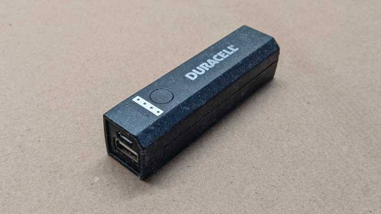

Contemplating options for powering my current project, I decided to repurpose an old USB power bank I bought nearly ten years ago. The primary problem with this device is that today’s devices expect more power than it could deliver. Specified to output up to one amp, I don’t think it could deliver that anymore. Most of my USB devices would cause it to shut down instead of charge. Another problem with this device is that its soft-touch outer plastic shell has become sticky. It is now impossible to keep clean and unpleasant to touch. It sat unused for several years in this state but now I have a potential use so I proceeded to violate the “Do Not Open” warning on the label.
There were no fasteners in the plastic shell to help disassembly, I just had to dig into seams and start prying it apart. Carefully, because puncturing a lithium-ion battery cell would be very bad news and electronics are still powered by said battery. (Use plastic tools!) Once the plastic shell was removed, we are left with the functional guts of the device:

The green cylinder is a lithium-ion battery cell in the very common 18650 (18mm diameter, 65mm length) form factor.

I’m not sure what MH27311 or ICR18650 meant exactly, but a web search found them sprinkled liberally across many eBay listings for lithium battery cells. I infer these were designations for a line of batteries that were popular enough to become eBay keyword salad. The next figure is the important one: nominal capacity of 2600 milliamp-hours. Nominal voltage of 3.7V is typical for lithium-ion cells. Finally, a date of December 2nd, 2013. This is probably the manufacturing date, though it would contradict the “Date: 2013-10” written on the outside label. Maybe it’s actually February 12th, 2013? Dates are hard.
Onward to the electronics, which were a pleasant surprise. They are two circuit boards connected to each other through two rows of four pins & sockets. I had expected a single circuit board or multiple circuit boards bonded together in some difficult-to-remove way. I didn’t expect nice easy pin and socket setup.
Here are the two sides of the first circuit board:


The top circuit board hosted the minimal user interface: four LEDs indicators (LED1 through LED4) and a push button (SW1). This side also has all of the designations printed on it: MS-B2600MPW-PC-A REV:A0 FR4 2013-5-4 26.3X18.5X1.2mm. The other side is dominated by an IC that presumably runs the show. I suspect it is a chip specifically designed to run a USB power bank, but there are no markings for me to investigate further. I also see globs of sturdy yellow material (epoxy?) that holds the chip in place as well as reinforcing the infamously fragile micro USB connector.
Here are the two sides of the second circuit board:


One side is dominated by connectors: one USB-A connector and two rows of four-pin connectors. Nestled between them is an electrolytic capacitor and soldering points for the battery cell labeled BT+ and BT-.
I thought I might see signs of damaged component somewhere that would explain the poor power output performance of this thing, but if present I don’t recognize them. That’s fine, I don’t intend to use the 5V output portion of this device anyway. I’ll quickly test the portions I actually need.
