Two Problems Controlling Buck Converter

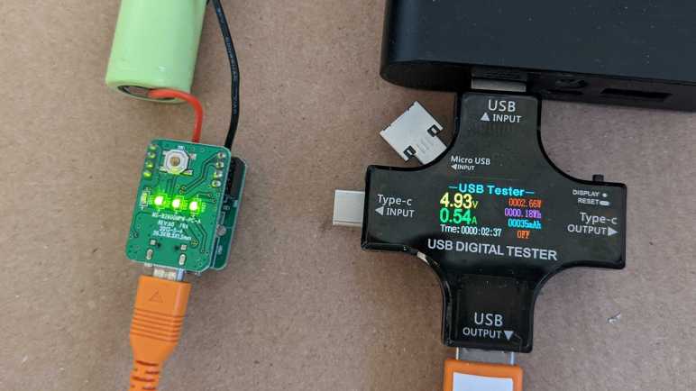
My solar power monitor project runs on a ESP8266 microcontroller and an INA219 sensor powered by an old USB power bank. In order to charge it during the day from solar power, I’m trying out a new-to-me buck converter module because it exposed an “Enable” pin that was absent from my usual MP1584 buck converter module. I connected it (via a 1k resistor) to the closest available GPIO pin on my ESP8266 module, which happened to be GPIO0. Configuring ESPHome to use that pin as a switch, I could turn charging on or off from Home Assistant UI. I declared victory but it was premature.

I realized there was a problem when I put the ESP8266 to sleep and noticed charging resumed. This was a surprise. Probing the circuit I found my first problem: there is a pull-up resistor or a voltage divider on board my new buck converter module so that if its enable pin is left floating, it will activate itself as my usual MP1584 module would. This was mildly disappointing, because it meant I might have to unsolder a few resistors to get the behavior I originally wanted, and one of the reasons to buy this module was because I didn’t want to unsolder resisters from my MP1584 buck converter boards. As a short-term hack, I fought the existing circuit by adding a pull-down resistor external to the module. Experimentally it looks like a 10k resistor to ground was enough to do the trick, disabling the buck converter when enable input line is left floating.

But I wasn’t done yet, there’s a second problem to address: When ESP8266 was put back in the circuit, the charging would still resume when I put it into deep sleep. Probing the pin, I saw GPIO0 was at 3.3V while asleep. Reading online resources like this page on Random Nerd Tutorials, I learned the pin needs to be high for ESP8266 to boot. Presumably this means the Wemos D1 Mini module has a pull-up resistor on board for the boot process. Therefore I can’t use GPIO0 for charging control.

I went down the list of still-unused pins by distance to the buck converter on my circuit board. The next closest pin is GPIO2, which I can’t use as I’m already using the blue status LED. After that is GPIO14. It is usually used for SPI communication but I have no SPI peripherals for this project. Looking on the reference chart, it doesn’t seem to get pulled up or down while ESP8266 was asleep. After confirming that behavior with a voltmeter, I switched buck converter enable pin over to GPIO14. It allowed me to control charging from ESPHome and, when the ESP8266 is asleep, the buck converter stays disabled. Finally, the hardware is working as intended! Now I need to figure out the software.

ESP8266 ADC Helps Avoid Over-Discharging Battery

I took apart a USB power bank so I could bypass its problematic power output circuit and run a Wemos D1 Mini module directly on the single lithium-ion battery cell. But bypassing the output circuit also means losing its protection against battery over-discharge. This could permanently damage a lithium-ion battery cell, so it is something I have to reimplement.

I can to use the only ADC (analog-to-digital conversion) peripheral on an ESP8266 to monitor battery voltage. The ESP8266 ADC is limited to sensing voltage in the range of zero to one volt, so a voltage divider is necessary to bring the battery’s maximum voltage level of 4.2V down to 1V. The Wemos D1 Mini module has a voltage divider already on board, using 220kΩ and 100kΩ resistors to (almost) bring 3.3V down to 1V. To supplement this, I added another 100kΩ resistor between battery positive and Wemos D1 Mini analog input pin.

For an initial test, I connected the analog input pin to my bench power supply and started adjusting power. It did not quite work as expected, reaching maximum value at a little over 4.1 volts. I suspect one or more of the resistors involved have actual resistance values different than advertised, which is normal with cheap resistors of 15% tolerance.

As a result, I could not sense voltage above 4.1V, which is probably fine for the purpose of over-discharge protection. But I was willing to put in a little extra effort to sense the entire range, and added another 10kΩ resistor in series for a total of 110kΩ between battery positive and the Wemos D1 Mini analog pin. This was enough to compensate for resistor tolerance and allow me to distinguish voltage all the way up to 4.2V.

To translate this divided voltage back to original input voltage, I recorded values from two voltage levels. I recorded what the ESP8266 ADC reported for each, and what I measured with my voltmeter. These data points allow me to use ESPHome Sensor component’s calibrate_linear filter to obtain values good enough to watch for battery over-discharge.

Here are the relevant excerpts from my ESPHome configuration YAML:

  - platform: adc
    pin: A0
    name: "Battery Voltage"
    filters:
      - calibrate_linear:
          - 0.84052 -> 3.492
          - 0.99707 -> 4.113
    on_value:
      then:
        - if:
            condition:
              sensor.in_range:
                id: battery_voltage
                below: 3.0
            then:
              - logger.log: "Battery critically low"
              - deep_sleep.enter:

Ideally, I would never reach this point. I should make sure the battery is adequately charged each day. I will need to drop voltage output of solar panel (up to 24V) down to the 5V input voltage expected by an USB power bank’s lithium-ion battery charging circuit, and I want to try a new-to-me buck converter module for the task.

Running Wemos D1 Mini ESP8266 On Single Lithium-Ion 18650 Cell

I’ve taken apart a broken USB power bank and the 18650 battery cell within has stayed within nominal range. Its battery and charging circuit looks good, or at least doesn’t do anything obviously bad with that battery. I take it as confirmation of my hypothesis that it’s the 5V boost output circuit that is broken, which is great because I plan to ignore that part.

I couldn’t quite decipher the exact voltage regulator used on board the Wemos D1 Mini clone I bought via Amazon. But from my time running these modules on weak AAs, they seem to behave like LDO (low-dropout regulator) in that they are happy to deliver 3.3V even if the input voltage hovers barely above 3.3V. And if the supply voltage drops even further, that is passed through instead of quitting or making weird noises like as a MP1584 buck converter did. As long as I keep this 18650 cell operating in the healthy range of 3V to 4.2V, I can wire it directly to the “5V” input pin on a Wemos D1 Mini module and it should deliver enough power to run an ESP8266 and INA219.

To mount the USB power bank circuit, I first looked at the existing pin headers hoping they’ll mount directly on a perforated prototype board with 0.1″ pitch. Sadly they are slightly narrower than that (2mm pitch?) and would not fit. However, the battery connectors are close enough to 0.3″ apart that I could solder 0.1″ header pins and mount that to the board. This is a perfect way to tap directly into the battery.

I cut up a small piece of plastic (expired credit card) to serve as insulation between circuit boards and from there it was straightforward to mount this on my prototype board. The battery cell is then soldered to these pins and temporarily secured with tape.

I was all ready to solder these pins directly to the Wemos D1 Mini as well, but then I realized doing so would leave no graceful way to cut power. So I added a pair of jumpers (one for BT+, one for BT-) allowing me to turn things off if needed. Once I finished soldering (and probing to verify I hadn’t shorted anything) I put the jumpers in and saw the blinking LED of an ESP8266 starting up. Success!

Bypassing the broken power output portion of this USB power bank puts this little piece of equipment back to work instead of tossing it in electronic waste. But it also meant I lost over-discharge protection so I will have to implement that myself.

USB Power Bank Charging Looks OK

I just took apart an old broken USB power bank to see if I can use it as a power source for an ESP8266 project. I needed to get inside to see if the parts I wanted are working properly. Broadly speaking, a USB power bank can be divided into three major pieces of functionality:

  1. Battery cell itself.
  2. Charging circuit, which typically accepts 5V USB power and charges the battery cell.
  3. Power delivery circuit, which takes battery power and boosts it to 5V USB power for delivery.

This particular USB power bank works for little LED trinkets but would shut itself down whenever I plug in something more substantial. I appreciate that it would gracefully shut down instead of doing something spicy like burst into flames, but it is not terribly useful as a USB power bank that way. Each of its major pieces might have caused this behavior:

  1. Battery cell could have gone bad, so as soon as any load is placed on the cell the voltage immediately drops below the low-power cutoff point.
  2. Charging circuit could have gone bad, failing to properly charge the battery.
  3. Power delivery circuit could have gone bad and unable to deliver specified power.

I hope it is the power delivery circuit, which is unsuitable for microcontroller project power supply even when it is fully functional due to the following:

  1. Charge or discharge, not both. When a power bank is charging through its input port, they usually shut down their output port. This is fine for the designed usage pattern of USB power banks, but it is obviously not good if I want my system to keep running while it is charging.
  2. Auto-Off: When a power bank senses that their load has dropped below some threshold, they automatically shut down their output port. Again this is fine for charging power-hungry devices and shutting off when they’re full. But when I’m trying to keep my ESP8266 power consumption low, I trigger the automatic shutoff.

Given the possibility that the boost converter power delivery circuit (which I didn’t want anyway) is the broken part, I hacked this one open to see if the battery cell and the charging circuits are still good. The first check is easy: a volt meter confirmed this cell is within the 3V to 4.2V range for healthy lithium-ion cells. (Unlike some past project.) Then I used another USB power bank to charge this battery. My USB tester measured charging rate at 4.93V * 0.54A = 2.66W. When bucking this down to 3.7V nominal voltage this would work out to 0.72A. Rule of thumb for charging lithium-ion chemistry battery is to charge at a rate no more than “0.5C to 1C”. This cell has an advertised capacity of 2600mAh, so “0.5C to 1C” is the range of 1.3A-2.6A. Thus ~0.72A is comfortably under that range and should be a relaxing charge for the battery.

Charging rate: check!

The next test is whether the charging circuit would stop charging at the correct point, so I left it charging until it stopped. Shortly after it stopped, my voltmeter measured 4.16V across the battery terminals. This is less than the 4.2V absolute maximum for lithium-ion cells.

Charging halt: check!

With these tests, I have some confidence the battery cell still works, and the charging circuit correctly limits the charging rate and maximum voltage. Good enough for me to try putting them to work.

USB Power Bank Teardown (Duracell DU7169)

Contemplating options for powering my current project, I decided to repurpose an old USB power bank I bought nearly ten years ago. The primary problem with this device is that today’s devices expect more power than it could deliver. Specified to output up to one amp, I don’t think it could deliver that anymore. Most of my USB devices would cause it to shut down instead of charge. Another problem with this device is that its soft-touch outer plastic shell has become sticky. It is now impossible to keep clean and unpleasant to touch. It sat unused for several years in this state but now I have a potential use so I proceeded to violate the “Do Not Open” warning on the label.

There were no fasteners in the plastic shell to help disassembly, I just had to dig into seams and start prying it apart. Carefully, because puncturing a lithium-ion battery cell would be very bad news and electronics are still powered by said battery. (Use plastic tools!) Once the plastic shell was removed, we are left with the functional guts of the device:

The green cylinder is a lithium-ion battery cell in the very common 18650 (18mm diameter, 65mm length) form factor.

I’m not sure what MH27311 or ICR18650 meant exactly, but a web search found them sprinkled liberally across many eBay listings for lithium battery cells. I infer these were designations for a line of batteries that were popular enough to become eBay keyword salad. The next figure is the important one: nominal capacity of 2600 milliamp-hours. Nominal voltage of 3.7V is typical for lithium-ion cells. Finally, a date of December 2nd, 2013. This is probably the manufacturing date, though it would contradict the “Date: 2013-10” written on the outside label. Maybe it’s actually February 12th, 2013? Dates are hard.

Onward to the electronics, which were a pleasant surprise. They are two circuit boards connected to each other through two rows of four pins & sockets. I had expected a single circuit board or multiple circuit boards bonded together in some difficult-to-remove way. I didn’t expect nice easy pin and socket setup.

Here are the two sides of the first circuit board:

The top circuit board hosted the minimal user interface: four LEDs indicators (LED1 through LED4) and a push button (SW1). This side also has all of the designations printed on it: MS-B2600MPW-PC-A REV:A0 FR4 2013-5-4 26.3X18.5X1.2mm. The other side is dominated by an IC that presumably runs the show. I suspect it is a chip specifically designed to run a USB power bank, but there are no markings for me to investigate further. I also see globs of sturdy yellow material (epoxy?) that holds the chip in place as well as reinforcing the infamously fragile micro USB connector.

Here are the two sides of the second circuit board:

One side is dominated by connectors: one USB-A connector and two rows of four-pin connectors. Nestled between them is an electrolytic capacitor and soldering points for the battery cell labeled BT+ and BT-.

I thought I might see signs of damaged component somewhere that would explain the poor power output performance of this thing, but if present I don’t recognize them. That’s fine, I don’t intend to use the 5V output portion of this device anyway. I’ll quickly test the portions I actually need.