Adafruit SSD1305 Arduino Library on ESP8266

Thanks to Adafruit publishing an Arduino library for interfacing with SSD1305 display driver chip, I proved that it’s possible to control an OLED dot matrix display from a broken FormLabs Form 1+ laser resin 3D printer. But the process wasn’t seamless, I ran into several problems using this library:

  1. Failed to run on ESP32 Arduino Core due to watchdog timer reset.
  2. 4 pixel horizontal offset when set to 128×32 resolution.
  3. Sketch runs only once on Arduino Nano 33 BLE Sense, immediately after uploading.

Since Adafruit published the source code for this library, I thought I’d take a look to see if anything might explain any of these problems. For the first problem of watchdog reset on ESP32, I found a comment block where the author notes potential problems with watchdog timers. It sounds like an ESP8266 is a platform known to work, so I should try that.

  // ESP8266 needs a periodic yield() call to avoid watchdog reset.
  // With the limited size of SSD1305 displays, and the fast bitrate
  // being used (1 MHz or more), I think one yield() immediately before
  // a screen write and one immediately after should cover it.  But if
  // not, if this becomes a problem, yields() might be added in the
  // 32-byte transfer condition below.

While I’m setting up an ESP8266, I could also try to address the horizontal offset. It seems a column offset of four pixels were deliberately added for 32-pixel tall displays, something not done for 64-pixel tall displays.

  if (HEIGHT == 32) {
    page_offset = 4;
    column_offset = 4;
    if (!oled_commandList(init_128x32, sizeof(init_128x32))) {
      return false;
    }
  } else {
    // 128x64 high
    page_offset = 0;
    if (!oled_commandList(init_128x64, sizeof(init_128x64))) {
      return false;
    }
  }

There was no comment to explain why this line of code was here. My best guess is the relevant Adafruit product has internally wired its columns with four pixels of offset, so this code makes a shift to compensate. If I remove this line of code and rebuild, my OLED displays correctly.

As for the final problem of running just once (immediately after upload) on an Arduino Nano 33 BLE Sense, I don’t have any hypothesis. My ESP8266 happily restarted this test sketch whenever I pressed the reset button or power cycled the system. I’m going to chalk it up to a hardware-specific issue with the Arduino Nano 33 BLE Sense board. At the moment I have no knowledge (and probably no equipment and definitely no motivation) for more in-depth debugging of its nRF52840 chip or Arm Mbed OS.

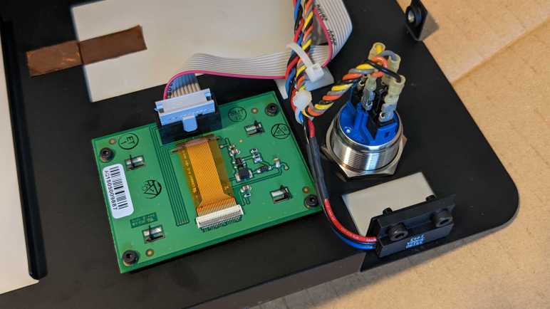
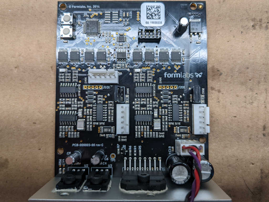
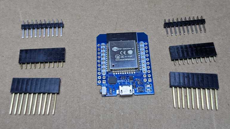
Now I have this OLED working well with an ESP8266, a hardware platform I have on hand, I can confidently describe this display module’s pinout.

First Test with Adafruit SSD1305 Library

I feel I now have a good grasp on how I would repurpose the OLED dot matrix display from a broken FormLabs Form 1+ laser resin 3D printer. I felt I could have figured out enough to play back commands captured by my logic analyzer, interspersed with my own data, similar to how I controlled a salvaged I2C LCD. But this exploration was much easier because a user on FormLabs forums recognized the SSD1305-based display module. Thanks to that information, I had a datasheet to decipher the commands, and I could go searching to see if anyone has written code to interface with a SSD1305. Adafruit, because they are awesome, published an Arduino library to do exactly that.

Adafruit’s library was written to support several of their products that used an SSD1305, including product #2675 Monochrome 2.3″ 128×32 OLED Graphic Display Module Kit which looks very similar to the display in a Form 1+ except not on a FormLabs custom circuit board. Adafruit’s board has 20 pins in a single row, much like the Newhaven Display board but visibly more compact. Adafruit added level shifters for 5V microcontroller compatibility as well as an extra 220uF capacitor to help buffer power consumption.

Since the FormLabs custom board lacked such luxuries, I need to use a 3.3V Arduino-compatible microcontroller. The most convenient module at hand (because it was used in my most recent project) happened to be an ESP32. The ssd1305test example sketch of Adafruit’s library compiled and uploaded successfully but threw the ESP32 into a reset loop. I changed the Arduino IDE Serial Monitor baud rate to 115200 and saw this error message repeating endlessly every few seconds.

ets Jun  8 2016 00:22:57

rst:0x8 (TG1WDT_SYS_RESET),boot:0x13 (SPI_FAST_FLASH_BOOT)
configsip: 0, SPIWP:0xee
clk_drv:0x00,q_drv:0x00,d_drv:0x00,cs0_drv:0x00,hd_drv:0x00,wp_drv:0x00
mode:DIO, clock div:1
load:0x3fff0030,len:1344
load:0x40078000,len:13516
load:0x40080400,len:3604
entry 0x400805f0
SSD1305 OLED test

Three letters jumped out at me: WDT, the watchdog timer. Something in this example sketch is taking too long to do its thing, causing the system to believe it has locked up and needs a reset to recover. One unusual aspect of ssd1305test code is that all work live in setup() leaving an empty loop(). As an experiment, I moved majority of code to loop(), but that didn’t fix the problem. Something else is wrong but it’ll take more debugging.

To see if it’s the code or if it is the hardware, I pulled out a different 3.3V microcontroller: an Arduino Nano 33 BLE Sense. I chose this hardware because its default SPI communication pins are those already used in the sample sketch, making me optimistic it is a more suitable piece of hardware. The sketch ran without triggering its watchdog dimer, so there’s an ESP32 incompatibility somewhere in the Adafruit library. Once I saw the sketch was running, I connected the OLED and immediately saw the next problem: screen resolution. I see graphics, but only the lower half. To adjust, I changed the height dimension passed into the constructor from 64 to 32. (Second parameter.)

Adafruit_SSD1305 display(128, 32, &SPI, OLED_DC, OLED_RESET, OLED_CS, 7000000UL);

Most of the code gracefully adjusted to render at 32 pixel height, but there’s a visual glitch where pixels are horizontally offset: the entire image has shifted to the right by 4 pixels, and what’s supposed to be the rightmost 4 pixels are shown on the left edge instead.

The third problem I encountered is this sketch only runs once, immediately after successful uploading to the Nano 33 BLE Sense. If I press the reset button or perform a power cycle, the screen never shows anything again.

Graphics onscreen prove this OLED responds to an SSD1305 library, but this behavior warrants a closer look into library code.

FormLabs Form 1+ OLED Screen Updates

It looks like the OLED dot matrix display in my broken FormLabs Form 1+ laser resin 3D printer uses a SSD1305 controller, based on communication traffic captured during its initial power-up sequence. Walking through that data while cross-referencing with the SSD1305 datasheet taught me a lot, and now I can apply this knowledge to examine logic analyzer traces from OLED reacting to other printer activities.

The Form 1+ doesn’t really have a power switch. When the 24VDC power supply is plugged in, it immediately starts running which includes the OLED power-up sequence I examined. But the user doesn’t see anything, because OLED display frame buffer has been filled with all black pixels. It’s not until they press the front panel button does the OLED start displaying visible pixels, and I have a logic analyzer trace of this startup sequence.

Visually, the startup sequence is a short animation of FormLabs text and butterfly logo. From off the bottom of the screen, it translates upwards until the text and logo is centered on screen for a brief second marking the end. From that point on, the screen is used to display up to four lines of text. Before this animation started, I see an initialization sequence identical to the power-up sequence: set all parameters and clear all eight memory pages to zero. After that, the animation starts running. When reading the SSD1305 datasheet, I saw it had a vertical scroll mode where bitmap in memory can be scrolled by changing the rendering start address. I thought that’s what the FormLabs animation used, but it wasn’t. Each frame of the animation is a full screen update sending four blocks of data for pages 0-3.

It appears memory pages 4-7 are not actively used for this application, which makes sense as the SSD1305 is designed for up to 132×64 pixels and we only have 128×32 on this OLED. However, those four pages of update data are transmitted in reverse order. Page 3 first, then 2, then 1, then 0. I wonder why? Hypothesis: This is to minimize visual artifacts. Imagine what happens if we update a memory page at the exact same time SSD1305 is displaying data from that page. We’d see a part of the old image mixed in with the updated image. Assuming the SSD1305 renders in increasing page order, sending data in the same increasing order means worst case unlucky timing will mess up all four pages. But if we update page in decreasing order, even the unluckiest timing scenario means only one out of four pages would be messed up.

Guesses or not, I feel like I have a pretty grasp of this OLED display module. Enough to try controlling it with my own code.

FormLabs Form 1+ OLED Control Consistent with SSD1305

I’ve been looking at various components of a broken FormLabs Form 1+ laser resin 3D printer, right now the focus is its front panel dot matrix OLED display. My first attempt at using a logic analyzer on its control signals told me which wires were active, but the actual data were gibberish. Fortunately, a second attempt retrieved sensical data waveforms. Someone on the FormLabs forums speculated this was an OLED display built around a SSD1305 controller, so now I will see if my captured data matches commands listed in SSD1305 documentation.

This stream of data represents system powerup, a set of commands (channel 0 white line is low) sent just before the first batch of data (channel 1 white line is high). If I interpret these bytes in context of SSD1305 datasheet, I get the following:

  • 0xAE: Display OFF.
  • 0xD5 0x10: Set display clock divide ratio to 1:1 and oscillator frequency to 300kHz.
  • 0xA8 0x1F: Set multiplex ratio to 31. (0x1F)
  • 0xD3 0x00: Set display offset to zero.
  • 0x40: Set display start line to zero.
  • 0xAD: Master Configuration for external Vcc power supply.
  • 0x8E: ???
  • 0x20 0x02: Set memory addressing mode to 0x02 (Page Addressing Mode.)
  • 0xA0: Set segment remap to 0 (Column address 0 is SEG0)
  • 0xC8: Set COM output scan direction to 1 (Remapped mode. Scan from COM[N~1] to COM0)
  • 0xDA 0x12: Set COM pins hardware configuration. (Disable COM Left/Right remap, Alternative COM pin configuration.)
  • 0x91 0x3F 0x3F 0x3F 0x3F: Set current drive pulse width of BANK0, color A, B, and C all to maximum valid value of 0x3F (63 clocks).
  • 0x81 0xFF: Set contrast control for BANK0 to 0xFF. (256, which is maximum contrast.)
  • 0x82 0xFF: Set brightness for area color banks to 0xFF. (256, which is maximum brightness.)
  • 0xD9 0xD2: Set precharge period to 0xD2. (Phase 1 period of 0x2 clocks, phase 2 period of 0xD or 13)
  • 0xDB 0x08: Set VCOMH Deselect Level to 0x08, but 0x08 is not in the list of valid values?
  • 0xA4: Entire display ON to display RAM content.
  • 0xA6: Set Normal Display. (Instead of 0xA7 for Inverted.)

This looks like an entirely sensible chain of commands for initial startup, aside from the two gaps: command 0x8E and parameter 0x08 for command 0xDB. The datasheet I have is rev 1.9 dated May 2008, so it’s possible those commands were added later. Even though they didn’t quite line up with the datasheet, these matches are too close to have been a coincidence. I’m now convinced there is a SSD1305 (or very closely related derivative) controller inside this OLED module.

Three more commands round out the end of the startup sequence:

  • 0xB0: Set Page Start Address to 0.
  • 0x00: Set Lower Column Start address to 0.
  • 0x10: Set Higher Column Start address to 0.

After these are sent, the Command/Data line was raised signifying data transmission. A large number of zeros followed, then the C/D line was lowered in for another trio of commands:

  • 0xB1: Set Page Start Address to 1.
  • 0x00: Set Lower Column Start address to 0.
  • 0x10: Set Higher Column Start address to 0.

Followed by another large chunk of zeroes, and this repeated for all eight pages of memory. Documentation section 8.7 Graphic Display Data RAM (GDDRAM) gave a size of 132 x 64 bits divided into eight pages. By that math, there should be 132 bytes in each block of zeros, but I’m not going to count that by hand. There’s probably a way to count inside Saleae Logic software, but I went with a low-tech approach:

  1. Zoom into the trace so one large block of zeros span majority of my computer monitor.
  2. Using a ruler, I measured the physical width on screen of the first eight decoded bytes of 0x00: they are 33mm wide.
  3. 132 bytes / 8 bytes = 16. So if there are 132 bytes in the block of zeros, they should be (16 * 33mm =) 528mm wide.
  4. I measured the entire block, 525mm wide. Close enough!

Having learned this information about initial startup including clearing the screen memory, I can better interpret the data captured by the logic analyzer during my other test activities.

Second Try with FormLabs Form 1+ Display Board Signals

One lasting memory I have from the movie Apollo 13 is the line “is this an instrumentation problem or are we looking at real power loss?” When an instrument tells us something is wrong, it’s possible the problem is in the instrument and not in the system it is measuring. I thought of this when I looked over the initial set of logic analyzer traces of data sent to an OLED display module. The traces superficially resembled SPI, but with many traits inconsistent with SPI. Before I dive into a rabbit hole of trying to figure out strange data, I wanted to make sure it isn’t an instrumentation problem.

The first thought was sampling rate. I gathered information for 8 channels because I had an 8-channel logic analyzer. But there’s a tradeoff. Sampling frequency drops as number of channels go up. For the base model Saleae Logic 8 that I have, polling all 8 channels drops it down to 25MS/s (25 million samples per second.) This might not be fast enough, because SPI peripherals could go all the way up to a clock rate of 50MHz. My first round of probing found only three wires with interesting activity, so dropping sampling down to 3 channels let me increase sampling rate to 100MS/s. Which is the minimum requirement to capture a 50MHz signal, but I doubt this OLED is running that fast. If this is a SSD1305 controller, its datasheet (Table 13-4 Serial Interface Timing Characteristics) lists a clock cycle time minimum of 250ns which translates to a maximum clock speed of 4 MHz. I figured even if it isn’t a SSD1305, it likely operates at similar speeds.

The next step was to redo all physical connections. I disconnected all eight probes and reconnected to reseat just the three channels I care about. I switched to a different USB cable for the Saleae, and I plugged it into a different computer that had two advantages: (1) it had a faster processor, and (2) I could connect to an onboard USB port. (I didn’t need a USB hub.)

This second set of traces look more like the SPI signal I expected, so my problem was indeed instrumentation. But the white line (channel 0, display input pin 3) is still clearly not an SPI chip select signal, as data transmission occurs both at high and low levels. What might it be? Looking into the SSD1305 datasheet, I saw its SPI mode required an extra pin labeled D/C#. This is the Data/Command control pin telling the OLED how to interpret incoming SPI traffic. If this line is low, SPI traffic will be interpreted as commands. If this line is high, SPI traffic will be interpreted as data. This could explain what I see, but for final confirmation I will examine the data to see if it’s consistent with SSD1305 communication.

First Look at FormLabs Form 1+ Display Board Signals

I’m working to understand the OLED dot matrix display from a broken FormLabs Form 1+ laser resin printer. It is hosted on a FormLabs custom circuit board and, after tracing through copper traces of that board, I have a candidate list of five wires for further investigation. When I went to attach my Saleae logic analyzer, I decided to attach probes to all eight unknown wires. (Out of ten wires total and I have identified two: the ground and 3.3VDC Vcc wires.) It wasn’t much extra effort and I was curious if anything was going on. I then captured traces for four activities:

  1. Power-on: when I plugged the 24VDC power supply into the printer.
  2. Startup: when I pressed the front panel button to start its logo animation, ending at the “lid is open” warning.
  3. Steady: Several seconds when the display stays at “lid is open” warning, with no updates.
  4. Ready/Open/Ready: Using a magnet, I toggled the display from “ready” to “cover open” and back to “ready” again.

Trace for “Steady” showed no activity at all. I had expected the system to refresh the display periodically regardless of update activity, but I just captured five seconds of silence. This is quite a contrast from the super chatty display from an AT&T CL84209 handset where I had 2569 messages within 10 seconds! Here I have nothing. Well, at least that was out of the way.

Trace for “Power-on” and “Startup” was interesting because it captured activity on two of the three wires that were unused. One looked like clock and another looked like data, so I asked Saleae Logic to treat them as I2C. They came back as valid I2C messages.

write to 0x48 ack data: 0x01 0x00 
write to 0x48 ack data: 0x00

Hypothesis: printer mainboard has an I2C peripheral bus and it’s been routed all the way to the OLED display module circuit board. I2C is not used by this particular display module, but the design gives FormLabs an option to switch to an I2C display module without changing the rest of printer hardware. In the meantime, a logic analyzer connected to the display module would see traffic on the I2C bus. By this hypothesis, such traffic is intended for other components instead of this display, so I’ll ignore it until/unless I discover a reason to revisit. [UPDATE: I found a NXP LM75B on the mainboard, an I2C temperature sensor that could answer to address 0x48.]

Back to the five wires of interest: three wires showed activity correlating with screen updates. I didn’t see any activity independent of screen update, so these wires might be a dedicated peripheral data line. If it is a peripheral bus, every other peripheral on the bus stayed quiet during my test set of activities. At first glance I thought this was SPI, but a closer look revealed behavior inconsistent with SPI.

  • Mainboard cable pin 3 — connected to logic analyzer channel 0 (white line) — showed infrequent level changes near the start of every activity. A good candidate for SPI “Chip Select” or Enable, except data transfers seem to happen both when it is low and when it is high. Which shouldn’t happen if it is indeed Enable.
  • Mainboard cable pin 4 — connected to logic analyzer channel 4 (yellow line) — shows regular level changes during every activity. A good candidate for SPI Clock, except the candidate data line changes within each “clock” pulse” which shouldn’t happen if it is indeed clock.
  • Mainboard cable pin 6 — connected to logic analyzer channel 5 (green line) — shows level changes at irregular bursts. A good candidate for SPI Data, except it pulses out of sync with “clock”.

If this is SPI, why does it look weird? If this is not SPI, what is it? I’ll have to check over my setup and try again.

FormLabs Form 1+ Display Board Routing

I’m working to understand the OLED dot matrix display from a broken FormLabs Form 1+ laser resin printer. Thanks to FormLabs user forums I have a lead on an OLED module that might be using the same OLED display. However, the OLED is hosted on a different circuit board. Publicly downloadable information exists for that board, so I will use it as a guide in my exploration.

On the printer mainboard, next to the DISPLAY label for this connector is a number 1. The closest pin appears to be system ground and the red wire in the ribbon cable. I will use that as the starting point for display input pin numbering.

Examining the front, I could see there’s a connection between pin 1 and majority of copper on this side of the circuit board, giving us a generous ground plane. The copper trace connecting to pin 2 is wider than any other on this board. It measures 3.26V DC when the system is powered up, making it the best candidate for power input. It feeds into the network of components mounted on this circuit board, which then has its own traces to the OLED. This is strongly suggestive of a power-related circuit. I measured those traces and found a few different higher voltages. Conclusion: these components implement a voltage boost converter.

Out of remaining eight wires in the ribbon cable, it seems like only five are used. Those five signals were routed together towards the OLED.

This diagram captures what I could determine by visually following traces of copper. On the other end of these traces is the sheet of yellow FPC. It has “1” printed on the right and “24” on the left, so I’ll happily use them as pin numbers. Using that system, I have a first draft for the OLED wires on that yellow FPC. Right to left in the above picture, they are: [UPDATE: added information from deciphered pinout.]

  1. NC (Not Connected)
  2. GND (Ground — connected to display input pin 1)
  3. GND
  4. NC (Only wire to visibly end inside the FPC.)
  5. 3.3V — connected to display input pin 2
  6. GND
  7. GND
  8. Display input pin 7 [UPDATE: SPI Chip Select (Active Low)]
  9. Display input pin 5 [UPDATE: Reset (Active Low)]
  10. Display input pin 3 [UPDATE: Command/Data Select]
  11. GND
  12. GND
  13. Display input pin 4 [UPDATE: SPI Clock]
  14. Display input pin 6 [UPDATE: SPI Data In (there is no SPI Data Out)]
  15. NC
  16. GND
  17. GND
  18. GND
  19. GND
  20. GND
  21. 9.0V supplied by boost converter
  22. 8.1V supplied by boost converter
  23. 12.6V supplied by boost converter
  24. NC

This explains the majority of wires going into this OLED module, leaving five unknowns that connected input IDC ribbon cable directly to OLED FPC. Those five wires will be the focus for further exploration and my Saleae logic analyzer will give me some insight as to what’s going on.

FormLabs Form 1+ Display Board Rev 01

Following wires on the mainboard in a broken FormLabs Form 1+ laser resin 3D printer, I found harnesses leading to several components mounted on the front panel. There is a sensor to detect if the lid is open. (Or more technically, if a magnet is nearby. A magnet is embedded in the lid.) There is also a button combined with embedded LED illumination. And finally, the dot matrix display.

When this printer boots up, a short logo animation is shown before proceeding to display text, indicating arbitrary dot matrix graphics capability and not restricted to alphanumeric character display of a built-in font. Which is great for flexibility but would also mean it is more complex to operate.

After removing four tiny hex screws I could pull the display circuit board free. (Promptly losing one of four plastic spacers between the circuit board and front panel.) Now I can confirm its blue color came directly from the display and not a tint imparted by front panel plastic window. We also see the circuit board is a FormLabs custom breakout board labeled with:

FORMLABS, INC.
DISPLAY BOARD REF 01
334056-01

But what is that module hosted by the board? I couldn’t see any identifying markings as-is. Maybe there are some on the back? The display module is held in place by four twisted rear metal tabs that I could straighten out with pliers, freeing the module.

I had noticed the pixel illumination didn’t look like backlit LCD, and here we see it very clearly marked as an OLED unit. Nice! Printed on the back were the following information:

PG-2832ALBM
P1471277-20-D14

And my search for that text came up with… nothing. Quite disappointing! I went on the internet to see if anyone else has identified this OLED module but didn’t find anything definitive. What I found was “Possible OLED display swap/spare” on the FormLabs user forums, posted by someone before they even received their Form 1 printer. They speculated it might be an NHD-2.23-12832UCB3 by Newhaven Display, which has a SS1305 controller. Sadly, they never returned to FormLabs forum to confirm their speculation, so I guess I’ll have to try that myself.

FormLabs circuit board has 10 IO pins in two rows of five. Newhaven Display’s website shows a very different breakout circuit board of 20 IO pins in a single row. But this difference could be explained. The display has very flexible IO configuration options: “This self-illuminating module has 6800/8080 parallel, serial SPI or I2C interface compatibility.” A custom FormLabs circuit board would only need to accommodate the interface they actually use in the product, ignoring pins for other interface options.

The collection of components on the FormLabs board looks broadly similar to the Newhaven board, though missing a few parts that could likewise be explained by supporting just data one interface instead of several. I would feel better if there’s a match between information printed on the OLED module itself and what’s listed on Newhaven Display website. But I felt more confident after looking at the thin FPC ribbon cable connecting the OLED to the circuit board: They are both 24-pins and have a very similar layout, including a truncated pin 4. Furthermore, they are both printed with the text:

E308847 F-D 1 94V-0

If these were two different displays, they’re using the same FPC ribbon cable so there’s a chance they use the same control protocols. Newhaven Display website says they welcome custom orders so maybe PG-2832ALBM is a FormLabs custom derivative of 2832UCB3? Either way, it is a promising starting point for a deeper look.

More FormLabs Form 1+ Mainboard IO

I turned on a broken FormLabs Form 1+ resin laser printer without its rear panel so I could poke around. I started with cables (POWER, X SIGNAL, Y SIGNAL) between its mainboard and galvanometer control board, because that’s where things broke. But now I have a better understanding (and even a long-shot idea to try) I came back to measure voltages of wires on the remaining mainboard connectors.

The Z-axis linear motion actuator (Z MOTOR) is driven by a bipolar stepper motor with two phases and two wires for each phase, the four wires labeled A+/A-/B+/B-. The resin tray peeling actuator (TILT MOTOR) is physically a very different motor but driven in the same style. Z-axis limit switch appears to be an optical interrupter which can be more accurate than the physical contact microswitch typically used for limit switch duty in FDM printers. It has three wires. One end has continuity to ground, the other end measured +5V while the printer is powered up. Middle wire measured 0.06V when Z-axis is positioned at top, and 3.7V when Z-axis is lowered.

As part of laser eye protection, the printer stops printing if we open the lid. Detecting this condition is the job of a (likely Hall effect) sensor just under the lid along with a magnet embedded in the lid. The magnet sensor plugs into the connector labeled INTERLOCK on the mainboard, with three wires colored black, blue, and red.

Wire ColorVolts DC (No magnet)Volts DC (Magnet nearby)
Black0V (Ground)0V (Ground)
Blue11.18V DC0.02V DC
Red11.18V DC11.18V DC

Speaking of that laser, I had hoped to see a diode module with two wires positive and ground. (Example*) But LASER connector actually had four wires: red, black, blue, and yellow.

Wire ColorLaser StandbyLaser Illuminated
Red11.18V DC11.18V DC
Black8.55V DC6.6V DC
Blue5V DC3.3V DC
Yellow0V (Ground)0V (Ground)

I’m sure those voltages aren’t the whole picture so if I have the ambition to drive this laser module myself, I have more investigation ahead.

Next connector is BUTTON for a gorgeous illuminated metal button on the front panel. Four wires support this button, two for the LED and two for the switch. Red wire is LED+, gray wire is LED- (wired to ground on this circuit board.) Yellow is pulled up to 3.3V on this board and when pressed, yellow wire shorts to black which is wired to ground.

The final connector is a little more complex. It is a 10-pin (2×5) IDC ribbon cable for the front panel display. Probing that display will be a project all by itself.


(*) Disclosure: As an Amazon Associate I earn from qualifying purchases.

Guesses on FormLabs Form 1+ Galvanometer Control Board

The laser galvanometers on this FormLabs Form 1+ resin laser printer no longer move, which rendered the printer useless. Probing voltage of wires leading to those galvanometers weren’t as enlightening as I had hoped but hinted that actuator position sensors were analog. Earlier probing of wires between printer mainboard and galvanometer control board, I also found mainboard commands were analog voltages.

With these analog inputs, I was confused by the fact I found no analog-to-digital converters among the list of ICs. The STM32 microcontroller has but a single ADC channel. And even if it had enough channels, I doubt they’d be fast or accurate enough. (Built-in ADC peripheral proved to be limited when I used a ESP32 to measure voltage, and when I used an ESP8266 to measure temperature.) I found many digital potentiometers and a two-channel SPI-controlled DAC for converting digital commands to analog voltage, but not the other way around.

I went online to look at other galvanometer control boards. Looking at this unit (*) and this unit (*) found a few commonalities. They have six wires leading to their galvanometers as well, hinting at a standardized system or at least a convention. I see they also want positive and negative supply voltages, which matches what I’ve seen. I also noticed they want different input voltage ranges, and their galvanometers don’t operate with the same mechanical ranges. (Movement in terms of degrees of rotation.) Dashing any hope of a direct replacement.

They also have 6 or 7 potentiometers on board for tuning, and this was my “A-ha!” moment. I saw similar potentiometers on the teardown of a Form 1, but such manual tuning potentiometers are missing here. This is what the STM32 and those digital potentiometers/SPI DAC are for: instead of manual tuning control with potentiometers, the upgraded Form 1+ galvanometer control board uses a STM32 to manage those parameters using those SPI-controlled digital potentiometers. The high-speed control loop is still an entirely analog process built out of those quad-pack op-amp chips.

Looking at this system with new knowledge, I see a tempting possibility. When I turn on the printer, I see a few brief LED flashes on the galvanometer control board as if STM32 booted up. Probing the 3.3V regulator (component U5) I saw it received +24VDC input and output the expected +3.3V DC for digital logic. Looking at the burned-out power connector, I saw the drama happened with the purple wire which I now know carried -24VDC. Perhaps this damage meant the board no longer has negative voltage and that’s why analog control system stopped working. What if I soldered the purple wire to some other location on the -24VDC plane? Say the input leg on one of two L79 negative voltage regulators? There’s a good chance it’ll only recreate the electrical fire, because I have not fixed the root cause of whatever caused that fire. But I see a slim chance rerouting -24VDC will get the galvanometers running again.

While I contemplate this potentially destructive experiment, I will look at other parts of this printer starting with the rest of those mainboard connectors.


(*) Disclosure: As an Amazon Associate I earn from qualifying purchases.

FormLabs Form 1+ Laser Galvanometer Voltages

I’m learning what I can from a broken FormLabs Form 1+ laser resin 3D printer, and it was instructive to probe voltage of wires between its (apparently functioning) mainboard and its (definitely toasted) galvanometer control board. Since I had my tools ready, I thought I’d take a look at voltages of wires leading to those galvanometers themselves. Even though they’re not moving anymore I had little to lose and hoped to learn something.

There weren’t many markings on these galvanometers. There are two stickers on both. On a flat end is a sticker with “ct-pass” probably for quality assurance during production. On the side of the cylinder is another sticker. One read “1411-0765 X” and the other “1411-0985 Y” Given that the X and Y axis are labeled, these are probably not part numbers. But what else would they be? Maybe something from the calibration process? I might see more markings if I remove these galvanometers from their aluminum mount, but I didn’t want to do that just yet. In the remote chance I could get things working, removing the galvanometers would ruin their factory direction calibration because I wouldn’t be able to put them back exactly in the same place.

Electrically speaking, from galvanometer Wikipedia page I knew a coil of wire to be involved, and there should be some way to read current position for closed-loop control. Examining the thin circuit board hosting the connector, I see the white and red wires on one end routed to one side together, a candidate for coil wires. Remaining four wires were routed together in a different direction, and I guess they are involved with position sensing in some way. Perhaps a high-resolution quadrature encoder? Or perhaps the four wires communicate position digitally via I2C or SPI? I did see a lot of chips on the control board communicate using SPI.

Turning the system on, I measured the following standby voltage values:

Wire ColorVolts DC
Yellow-0.044
Red-0.026
White+1.328
Black0.015
Red0.015
White0.040

Not terribly informative by themselves, sadly. I didn’t want to probe these voltages while the laser is shining, out of concern for my eyeballs. But I was curious to test my hypothesis of position sensing. Using fine-tipped tweezers, I rotated the output shaft while watching voltage values. The yellow wire showed a tiny change that correlated to shaft position: from -0.014V to -0.078V. The adjacent red wire showed a larger range, from 0.044V to -0.235V, also correlated to shaft position. Both of these are tiny changes in voltage, but the fact there’s a repeatable correlation of voltage rules out quadrature encoder or digital data communication. This is an analog position sensor of some type. If it were like potentiometers I’ve dealt with, then at one end of the range of motion either yellow or red wire should get up to +1.328V provided by a white wire. But it didn’t, so something else is going on. These observations aren’t enough for me to fully understand workings of this board, but enough for me to formulate a few guesses.

FormLabs Form 1+ Laser Galvanometer Control

Despite some concerns, I’ve decided to poke around inside a broken FormLabs Form 1+ laser resin 3D printer while it is running. I think it’ll tell me more about how it was supposed to work, because I didn’t learn very much from just a roster of ICs. But it still wouldn’t tell me everything, because some of its current behavior would be as intended while other behavior would be wrong because the printer is broken. And as my only example of the species, it might be hard to tell which is which.

Before I powered it up, I probed around for all the ground wires. Since the printer is powered by 24V DC delivered through a standard barrel jack, it was least easy to probe for continuity to ground. There was even an exposed pad on the main processor board labeled GND. Knowing which wire is ground for each connector established a baseline for voltage measurements once I turned the printer on.

The first surprise was on the GALVO POWER connector. It had three wires colored red, black, and purple. Black was known to be ground. Red was expected to be +24V DC, which was confirmed. I didn’t know what to expect for purple, and it turned out to be -24V DC. Negative voltage! Something I rarely see but it would be consistent with the presence of a ST Micro L79 negative voltage regulator delivering -15V. Which is a mirror match for the L78 positive regulator taking +24V DC and delivering +15V DC. Separately there is an On Semi NCP1117 delivering 3.3V for digital logic.

As for GALVO SIGNAL, it had three wires colored black, white, and red. Again I knew black was ground from earlier probing. Once the system was powered on, I saw white wire voltage stayed pretty consistent at 2.5V DC. The red wire was where interesting things happened: It varied between 0V to 5V relative to ground (or -2.5V to +2.5V relative to white wire) while this printer went through the motion of printing, blissfully unaware its galvanometer control system was fried. Plotting X and Y galvo signals against each other on my oscilloscope’s XY mode, it sure looks like a laser draw path. That is, as long as we ignore that diagonal noise I blame on my beginner level oscilloscope skill. Anyway, noise aside, it shows this 0-5V (Or -2.5 to +2.5V) analog voltage is how mainboard commands galvo position. This scorched control board couldn’t translate those commands into galvanometer movement, but I wanted to see if anything is getting to those galvanometers at all.

Considerations Exploring FormLabs Form 1+ While Powered Up

Curious about what I could learn from a scorched laser galvanometer control board, I looked up all component markings I could find. That gave me a few pieces of a puzzle, but I’m missing many more pieces and I don’t have a guess as to how those pieces fit together. In the interest of getting more data, I thought I would probe around while this FormLabs Form 1+ printer is powered up.

The biggest danger is a laser at the heart of this laser resin printer. This whole printer is classified as a Class 1 laser device, which means it is safe to use without eye protection. But that guarantee of safety only applies when used as intended. If I’m going to probe its circuitry with panels removed, I lose protection provided by those panels. Bypassing such protection means I have to be careful not to damage my eyes. Anyone who plans to try this as well: please be careful!

Working with lasers is especially dangerous if they operate at a wavelength outside human visible spectrum. We have evolved a blink reflex to protect our vision, but it wouldn’t work for wavelengths we can’t see. Thankfully, 405nm is within human visible spectrum (it should show up as an intense blue or violet beam), so I still have my blink reflex as a final line of defense. Why 405nm? Apparently, this wavelength became popular because Blu-ray drives drove R&D and economies of scale. I don’t know about power levels, though. I would guess resin printing runs 405nm lasers at a higher power level than reading Blu-ray discs (60mW as per Wikipedia) but I have no data to support that guess.

There’s another interesting data point I want to investigate: the printer was happy to run through its printing process with a dead galvanometer control board. Such behavior tells me something is running as an open-loop process, operating without feedback that its laser beam wasn’t being steered. I knew stepper motors used in cheap FDM 3D printers are open-loop devices, where the printer control board sends motor pulses without knowing if there is actual physical motion. But laser galvanometers are closed-loop actuators, so something else is going on.

Despite my wariness of a laser operating at unknown power levels, my curiosity motivated me to power it up and poke around.

Form 1+ Galvanometer Control Board IC Roll Call

This Form 1+ laser resin printer has a scorched galvanometer control board, and replacements are no longer available from FormLabs. I don’t have any background to make heads or tails of a laser galvanometer control board, but I might get a vague idea and learn something by examining its collection of components. Here’s a roll call based on markings on those chips.

The board controls both X and Y axis galvanometers, probably why the middle section of this board a pair of identical assemblies.

Starting from the upper left, component U4 looks to be the brains of this operation: a ST Microelectronics STM32F030K6T6 with its ARM Cortex-M0 core running at up to 48MHz.

U5 in the upper right is an On Semiconductor NCP1117, a low-dropout (LDO) voltage regulator marked with 17-33G indicating it outputs 3.3V. This would supply power to the STM32 and other 3.3V digital logic.

Back towards the centerline, U6 is a Microchip MCP4802 digital-to-analog converter (DAC) with dual 8-bit resolution channels controlled via SPI.

Just below that is U7, a TI TL032 dual-channel op-amp.

On either side of U7 is a collection of 8 chips, four on each side. (U104, U105, U106, and U107 on the left. U204, U205, U206, and U207 on the right.) They are all marked with Microchip logo and 41H51103, which I found to be a MCP41HV51 SPI-controlled digital potentiometer. In section 11.1 Package Marking Information of the MCP41HVx1 datasheet, 41H51103 is identified as MCP41HV51-103E/ST variant.

There are a lot of surface mount passives in the center section with two copies of the layout left and right. Each copy gets a trio of chips marked with On Semiconductor logo and MC33274ADG. These MC33274A chips are each a quad-pack of op-amps. Each side has an additional component that is mounted vertically so we only see their top here.

Going back to an earlier picture focused on the burnt and melted connector, we can see one of those vertical standing components clearly on the right. They are On Semiconductor BD139 NPN power transistors.

Three components are bolted to a heat sink at the bottom. To the left is a single Texas Instruments LM1876. It is a dual 20W audio power amplifier. Adjacent to that amplifier are a mirror pair of ST Microelectronics voltage regulators. The L79 negative voltage regulator accept up to -35V DC and output a regulated -15V DC. L78 is its symmetric positive voltage sibling, accepts up to +35V DC and output a regulated +15V DC.

Those components are major pieces of my “how did this board work” puzzle, but I’m still fuzzy on how they fit together. If I want more data, I’ll have to probe around while the system is powered up and I’m not entirely sure I want to do that.

FormLabs Form 1+ Next Steps

Diagnosing why a FormLabs Form 1+ resin laser 3D printer wasn’t working; I found the smoke trail of an electrical fire on its galvanometer (galvo) control board. This board is cooked in a very literal sense. Even though the printer is long out of support, I contacted FormLabs hoping for a replacement board. While waiting for a response, I took the printer apart to get a closer look at the damaged board.

It looks far worse from this angle. A lot of charred and burnt plastic at the base of power connector, which had melted together into a single lump. It is no longer possible to (neatly) unplug this connector. A surface-mount capacitor C20 has been vaporized along with some of the circuit board creating a small pit.

Holding the board at a different angle, I saw charred residue of smoke trail running all the way up the board. This fire was more significant than I had previously thought. This is good news and bad news. I had been worried that I cooked the device with a nonstandard power supply but seeing extent of damage confirmed it happened before I got my hands on the device. If it happened on my watch, I would have definitely smelled dead electronics, a scent I was reminded of quite recently.

On the downside, severity of this damage puts repair out of reach of my current skill level. I don’t know anything about how galvanometer control circuits are supposed to work. My electronics engineering skills aren’t good enough to reverse engineer this board and fix it without technical information like schematics and diagnostics procedures.

After this (very discouraging) sight, FormLabs got back to me: no replacement galvo control boards are available. Unsurprising but at least it didn’t hurt to ask. I briefly considered buying a laser light show galvanometer setup from eBay or Amazon. But even if I could interface them, I don’t know how to test and tune them for good resin prints. Given these challenges, I’m not going to try to get this printer printing. I’ll focus on learning as much as I can from taking it (further) apart.

Switching to CPU Ticks Did Not Eliminate Wobble Because Fan Itself Was Wobbling

In order to obey constraints imposed by ESP32 hardware timer peripheral, I switched my fan strobe LED code to use a regularly polling interrupt service routine (ISR). I worried that I would be overly demanding to schedule it once every 10 microseconds, but I saw no obvious problems from that front. What I did see, though, is an irregular wobble at longer LED pulse delays indicating my LED strobe timing is drifting in and out of sync with fan blade position.

Because I had calculated timing for LED pulses by counting number of times my ISR is executed, I thought this wobble might be caused by unpredictable delays in ISR overhead. A multi-millisecond strobe delay (where I notice the wobble) would require my ISR to count several hundred times, allowing tiny errors to add up. To test this hypothesis, I switched my code to use a more consistent timing mechanism: the ESP32 CPU tick counter. It is a highly precise (though not necessarily accurate) source of timing information, one that I used for performance metrics in ESP_8_BIT_Composoite. But it comes with limitations including:

  • Tick counter value is only valid on the same core it is queried from, it is not valid to compare tick count across the two cores of an ESP32. Not a problem here because Arduino subsystem is pinned to a single core, so I am guaranteed to always be on the same core.
  • It goes up by one for each clock cycle of the CPU core. At 240MHz, an unsigned 32-bit value would overflow two or three times every minute. For this quick experiment I’m ignoring overflows, resulting in a brief dark pulse two or three times per minute. (This limitation was why I didn’t use it in my first draft.)

Switching my timer counter to CPU ticks did not eliminate the wobble, disproving my hypothesis. What else could it be? Thinking through possible explanations, I wished I could see exact time relationship between tachometer signal and my LED strobe pulses. Then I remembered I could do exactly that because I have a real oscilloscope now! In fact, I should have put it on scope before embarking on my CPU clock tick counter experiment. I guess I’m still not used to having this powerful tool at hand.

I set up the oscilloscope so I could see the fan tachometer pulse that would trigger my tachometer interrupt handler, where I calculate the ticks for turning LED on and off. I set up the oscilloscope to trigger on my resulting LED output pulse. I increased the LED pulse delay to roughly 6 milliseconds, which is a roughly 180 degree rotation. Placing that pulse close to the next fan tachometer pulse allowed me to easily compare their timing on oscilloscope screen.

As it turned out, my ESP32 code is completely blameless. The timing held steady between tachometer signal triggering pulse and LED output pulse. What changed are timing between consecutive fan tachometer pulses. In other words: my strobe light visual is wobbling because fan speed is wobbling. This is exactly why strobe lights are useful to diagnose certain problems with high-speed machinery: it makes subtle problems visible to the human eye.

Conclusion: the wobble is not a bug, it is a feature!


Custom component code using CPU tick counter. (Does not account for 32-bit tick overflow):

#include "esphome.h"
#include "esp_system.h"

volatile int evenOdd;
volatile int strobeDuration;
volatile int strobeDelay;
volatile uint32_t ccountTachometer;
volatile uint32_t ccountLEDOn;
volatile uint32_t ccountLEDOff;

const int gpio_led = 23;
const int gpio_tach = 19;

// How many cycles per microsecond. 240 for typical ESP32 speed of 240MHz.
const int clockSpeed = 240;

hw_timer_t* pulse_timer = NULL;

IRAM_ATTR void pulse_timer_handler() {
  uint32_t ccountNow = xthal_get_ccount();

  if (ccountNow >= ccountLEDOn) {
    digitalWrite(gpio_led, HIGH);
    ccountLEDOn = 0;
  }

  if (ccountNow >= ccountLEDOff) {
    digitalWrite(gpio_led, LOW);
    ccountLEDOff = 0;
  }
}

IRAM_ATTR void tach_pulse_handler() {
  if (0 == evenOdd) {
    evenOdd = 1;
  } else {
    if (strobeDuration > 0 && ccountLEDOn == 0 && ccountLEDOff == 0) {
      ccountTachometer = xthal_get_ccount();

      // Calculate time for turning LED on and off
      ccountLEDOn = ccountTachometer + strobeDelay * clockSpeed;
      ccountLEDOff = ccountLEDOn + strobeDuration * clockSpeed;
    }
    evenOdd = 0;
  }
}

class FanStrobeLEDSetupComponent : public Component {
  public:
    void setup() override {
      // Initialize variables
      strobeDelay = 10;
      strobeDuration = 20;
      ccountLEDOn = 0;
      ccountLEDOff = 0;

      // LED power transistor starts OFF, which is LOW
      pinMode(gpio_led, OUTPUT);
      digitalWrite(gpio_led, LOW);

      // Attach interrupt to tachometer wire
      pinMode(gpio_tach, INPUT_PULLUP);
      evenOdd = 0;
      attachInterrupt(digitalPinToInterrupt(gpio_tach), tach_pulse_handler, RISING);

      // Configure hardware timer
      pulse_timer = timerBegin(0, 80, true);
      timerAttachInterrupt(pulse_timer, &pulse_timer_handler, true);
      timerAlarmWrite(pulse_timer, 10, true /* == autoreload */);
      timerAlarmEnable(pulse_timer);
    }
};

class FanStrobeLEDEvenOddToggleComponent: public Component, public Switch {
  public:
    void write_state(bool state) override {
      evenOdd = !evenOdd;
      publish_state(state);
    }
};

class FanStrobeLEDDelayComponent: public Component, public FloatOutput {
  public:
    void write_state(float state) override {
      strobeDelay = 11000*state;
    }
};

class FanStrobeLEDDurationComponent: public Component, public FloatOutput {
  public:
    void write_state(float state) override {
      strobeDuration = 1000*state;
    }
};

Polling ESP32 Timer Shows Wobble

I wanted to use my fan strobe LED as a learning project to work with ESP32 hardware timers, but my original idea required modifying timer configuration from inside a timer alarm ISR. I have learned that is not allowed, and I have the crash stacks to prove it. The ESP32 Arduino Core timer API is geared towards timer alarm interrupts firing at regular intervals to run the same code repeatedly, so I should change my code structure to match.

Since the tachometer signal timing, strobe delay, and strobe duration could all change at runtime, I couldn’t use any of those factors as my hardware timer interval. Switching to a regular timing interval meant I would have to poll current status to determine what to do about state of LED illumination.

For the first draft, I kept a counter of how many times my ISR has executed. This variable is only updated by the ISR. Based on this counter value, each tachometer ISR calculates the time for LED to be turned on and back off in terms of timer ISR counter. Timer ISR compares those values to turn the LED on, then back off. When a particular pulse is complete, the timer ISR resets all counters to zero and waits for the next tachometer pulse to occur.

I tried a timer ISR duration of polling once every 20 microseconds. This meant a worst-case scenario of LED pulse starting as much as 20 microseconds later than specified, and a pulse duration as much as 20 microseconds longer than specified. When the ideal duration is around 200-250 microseconds, this is nearly 10% variation and resulted in visible flickering. I then tried 10 microseconds, and the flickering became less bothersome. On an ESP32 running at 240MHz, it meant I demand my ISR run once every 2400 clock cycles. I’m worried this is too demanding, but I don’t have a better idea at the moment. At least it hasn’t crashed my ESP32 after several minutes of running.

This new mechanism also allowed me to increase my LED strobe delay beyond a millisecond, but I noticed an irregular wobbling for longer delays. Those strobes of light are not happening at my calculated location. They vary by only a few degrees but very definitely noticeable. Is this a sign that my ISR is too demanding? For a multi-millisecond LED strobe delay, a 10-microsecond timer ISR would execute hundreds of times. If there’s a tiny but unpredictable amount of delay on each, they might add up to cause a visible wobble. Perhaps I should use a different counter with better consistency.


Custom component code with timer counter:

#include "esphome.h"
#include "esp_system.h"

volatile int evenOdd;
volatile int strobeDuration;
volatile int strobeDelay;
volatile int timerCount;
volatile int timerLEDOn;
volatile int timerLEDOff;

const int gpio_led = 23;
const int gpio_tach = 19;

hw_timer_t* pulse_timer = NULL;

IRAM_ATTR void timerCountersReset() {
  timerCount = 0;
  timerLEDOn = 0;
  timerLEDOff = 0;
}

IRAM_ATTR void pulse_timer_handler() {
  if (timerCount >= timerLEDOn) {
    digitalWrite(gpio_led, HIGH);
  }

  if (timerCount >= timerLEDOff) {
    digitalWrite(gpio_led, LOW);
    timerCountersReset();
  } else {
    timerCount++;
  }
}

IRAM_ATTR void tach_pulse_handler() {
  if (0 == evenOdd) {
    evenOdd = 1;
  } else {
    if (timerLEDOn == 0 && strobeDuration > 0) {
      // Calculate time for turning LED on and off
      timerLEDOn = timerCount + strobeDelay;
      timerLEDOff = timerLEDOn + strobeDuration;
    }
    evenOdd = 0;
  }
}

class FanStrobeLEDSetupComponent : public Component {
  public:
    void setup() override {
      // Initialize variables
      strobeDelay = 10;
      strobeDuration = 20;
      timerCountersReset();

      // LED power transistor starts OFF, which is LOW
      pinMode(gpio_led, OUTPUT);
      digitalWrite(gpio_led, LOW);

      // Attach interrupt to tachometer wire
      pinMode(gpio_tach, INPUT_PULLUP);
      evenOdd = 0;
      attachInterrupt(digitalPinToInterrupt(gpio_tach), tach_pulse_handler, RISING);

      // Configure hardware timer
      pulse_timer = timerBegin(0, 80, true);
      timerAttachInterrupt(pulse_timer, &pulse_timer_handler, true);
      timerAlarmWrite(pulse_timer, 10, true /* == autoreload */);
      timerAlarmEnable(pulse_timer);
    }
};

class FanStrobeLEDEvenOddToggleComponent: public Component, public Switch {
  public:
    void write_state(bool state) override {
      evenOdd = !evenOdd;
      publish_state(state);
    }
};

class FanStrobeLEDDelayComponent: public Component, public FloatOutput {
  public:
    void write_state(float state) override {
      strobeDelay = 1100*state;
    }
};

class FanStrobeLEDDurationComponent: public Component, public FloatOutput {
  public:
    void write_state(float state) override {
      strobeDuration = 100*state;
    }
};

ESP32 Timer ISR Not Allowed to Call Timer API

Conceptually I knew using delayMicroseconds() inside an interrupt service routine (ISR) was a bad idea. But I tried it anyway on an ESP32 and now I have a crash stack to prove it was indeed a bad idea. A solid reason to switch over to using hardware timers. My fan strobe LED project has two needs: the first delay is between tachometer wire signal and turning LED on (this delay may be zero) followed by a second delay before turning LED back off. Duration of both of these delays vary in order to produce desired visual effects. Translating this concept directly into timers results in this pseudocode:

  1. Interrupt handler triggered by tachometer signal. Starts timer that calls step 2 when first it ends.
  2. Interrupt handler triggered by expiration of first delay. Turn on LED and start timer that calls step 3 when it ends.
  3. Interrupt handler triggered by expiration of second delay, turn off LED.

Unfortunately, that direct translation doesn’t work. At least not with ESP32 Arduino Core Timer APIs. The timer alarm callback (“call step 2” and “call step 3” above) is specified at the time an alarm timer is configured, and not something I can change in between steps 2 and 3 above. Furthermore, I had no luck changing the timer duration in between calls, either. Either the change has no effect (duration doesn’t change) or the timer alarm interrupt stops triggering entirely. The only way I got something resembling my initial pseudocode is to tear down and rebuild a timer on every call to step 1, then do it again on step 2, and repeat.

That code felt wrong, and it didn’t take long for me to see concrete evidence it was wrong. I could adjust my delay parameters a few times, but within 2-3 minutes of running this sketch my ESP32 would crash with the following stack:

WARNING Found stack trace! Trying to decode it
WARNING Decoded 0x40088dcc: invoke_abort at /home/runner/work/esp32-arduino-lib-builder/esp32-arduino-lib-builder/esp-idf/components/esp32/panic.c:715
WARNING Decoded 0x40089049: abort at /home/runner/work/esp32-arduino-lib-builder/esp32-arduino-lib-builder/esp-idf/components/esp32/panic.c:715
WARNING Decoded 0x40089dbf: xQueueGenericReceive at /home/runner/work/esp32-arduino-lib-builder/esp32-arduino-lib-builder/esp-idf/components/freertos/queue.c:2038
WARNING Decoded 0x400f1001: removeApbChangeCallback at /data/cache/platformio/packages/framework-arduinoespressif32/cores/esp32/esp32-hal-cpu.c:224
WARNING Decoded 0x400817f9: timerEnd at /data/cache/platformio/packages/framework-arduinoespressif32/cores/esp32/esp32-hal-timer.c:174
WARNING Decoded 0x40081095: pulse_off_handler() at /config/esphome/.esphome/build/fan-strobe-led/src/esphome/core/gpio.h:62
WARNING Decoded 0x400814c9: __timerISR at /data/cache/platformio/packages/framework-arduinoespressif32/cores/esp32/esp32-hal-timer.c:174
WARNING Decoded 0x400874cd: _xt_lowint1 at /home/runner/work/esp32-arduino-lib-builder/esp32-arduino-lib-builder/esp-idf/components/freertos/xtensa_vectors.S:1154
WARNING Decoded 0x4008568d: esp_dport_access_int_abort at /home/runner/work/esp32-arduino-lib-builder/esp32-arduino-lib-builder/esp-idf/components/esp32/dport_access.c:216
WARNING Decoded 0x40087e63: spi_flash_enable_interrupts_caches_and_other_cpu at /home/runner/work/esp32-arduino-lib-builder/esp32-arduino-lib-builder/esp-idf/components/spi_flash/cache_utils.c:203
WARNING Decoded 0x4008857a: spi_flash_guard_end at /home/runner/work/esp32-arduino-lib-builder/esp32-arduino-lib-builder/esp-idf/components/spi_flash/flash_ops.c:172
 (inlined by) spi_flash_read at /home/runner/work/esp32-arduino-lib-builder/esp32-arduino-lib-builder/esp-idf/components/spi_flash/flash_ops.c:664
WARNING Decoded 0x401659c9: nvs::nvs_flash_read(unsigned int, void*, unsigned int) at /home/runner/work/esp32-arduino-lib-builder/esp32-arduino-lib-builder/esp-idf/components/nvs_flash/src/nvs_ops.cpp:76
WARNING Decoded 0x40164289: nvs::Page::readEntry(unsigned int, nvs::Item&) const at /home/runner/work/esp32-arduino-lib-builder/esp32-arduino-lib-builder/esp-idf/components/nvs_flash/src/nvs_page.cpp:871
WARNING Decoded 0x401642fd: nvs::Page::eraseEntryAndSpan(unsigned int) at /home/runner/work/esp32-arduino-lib-builder/esp32-arduino-lib-builder/esp-idf/components/nvs_flash/src/nvs_page.cpp:871
WARNING Decoded 0x40164979: nvs::Page::eraseItem(unsigned char, nvs::ItemType, char const*, unsigned char, nvs::VerOffset) at /home/runner/work/esp32-arduino-lib-builder/esp32-arduino-lib-builder/esp-idf/components/nvs_flash/src/nvs_page.cpp:871
WARNING Decoded 0x4016337a: nvs::Storage::eraseMultiPageBlob(unsigned char, char const*, nvs::VerOffset) at /home/runner/work/esp32-arduino-lib-builder/esp32-arduino-lib-builder/esp-idf/components/nvs_flash/src/nvs_storage.cpp:579
WARNING Decoded 0x40163751: nvs::Storage::writeItem(unsigned char, nvs::ItemType, char const*, void const*, unsigned int) at /home/runner/work/esp32-arduino-lib-builder/esp32-arduino-lib-builder/esp-idf/components/nvs_flash/src/nvs_storage.cpp:579
WARNING Decoded 0x40162b3b: nvs_set_blob at /home/runner/work/esp32-arduino-lib-builder/esp32-arduino-lib-builder/esp-idf/components/nvs_flash/src/nvs_api.cpp:547
WARNING Decoded 0x400d8407: esphome::esp32::ESP32Preferences::sync() at /config/esphome/.esphome/build/fan-strobe-led/src/esphome/components/esp32/preferences.cpp:124
WARNING Decoded 0x400e35dd: esphome::preferences::IntervalSyncer::on_shutdown() at /config/esphome/.esphome/build/fan-strobe-led/src/esphome/core/gpio.h:62
WARNING Decoded 0x400e3665: std::_Function_handler<void (), esphome::preferences::IntervalSyncer::setup()::{lambda()#1}>::_M_invoke(std::_Any_data const&) at /config/esphome/.esphome/build/fan-strobe-led/src/esphome/core/gpio.h:62
WARNING Decoded 0x400e34e6: std::function<void ()>::operator()() const at /data/cache/platformio/packages/toolchain-xtensa32/xtensa-esp32-elf/include/c++/5.2.0/functional:1710
 (inlined by) esphome::Scheduler::call() at /config/esphome/.esphome/build/fan-strobe-led/src/esphome/core/scheduler.cpp:204
WARNING Decoded 0x400e1319: esphome::Application::loop() at /config/esphome/.esphome/build/fan-strobe-led/src/esphome/core/application.cpp:69
WARNING Decoded 0x400e391e: loop() at /config/esphome/.esphome/build/fan-strobe-led/src/esphome/core/gpio.h:62
WARNING Decoded 0x400f0e29: loopTask(void*) at /data/cache/platformio/packages/framework-arduinoespressif32/cores/esp32/main.cpp:23
WARNING Decoded 0x4008a05a: vPortTaskWrapper at /home/runner/work/esp32-arduino-lib-builder/esp32-arduino-lib-builder/esp-idf/components/freertos/port.c:355 (discriminator 1)

I’m not sure what removeApbChangeCallback() meant. I found the code, but there were no code comments explaining what “Apb” is. A general web search found one potential explanation of “Advanced Peripheral Bus“. Whatever it is, it was called as part of a FreeRTOS queue receive. This was a surprise. I know FreeRTOS queues can be used from inside an ISR to schedule work to be performed outside an ISR, but that would be an ISR-safe queue send, not a receive. Hitting a receive path inside an ISR feels wrong.

Looking further down the call stack, I see NVS (nonvolatile storage) calls like I saw when I failed to use delayMicroseconds() on the stack. Why are storage APIs being called? I didn’t look into it earlier, hoping I could avoid the problem by moving to timers, but it’s clear I need to better understand what’s going on. Poking around in ESPHome code, I believe this is trying to save state of my parameters so it could be restored in case of system reset or shutdown. If so, I should be able to deactivate such behavior by setting restore_mode parameter to ALWAYS_OFF.

WARNING Found stack trace! Trying to decode it
WARNING Decoded 0x400f0ea8: initApbChangeCallback at /data/cache/platformio/packages/framework-arduinoespressif32/cores/esp32/esp32-hal-cpu.c:224
WARNING Decoded 0x400817e2: timerBegin at /data/cache/platformio/packages/framework-arduinoespressif32/cores/esp32/esp32-hal-timer.c:174
WARNING Decoded 0x4008110c: tach_pulse_handler() at /config/esphome/.esphome/build/fan-strobe-led/src/esphome/core/gpio.h:62
WARNING Decoded 0x40081185: __onPinInterrupt at /data/cache/platformio/packages/framework-arduinoespressif32/cores/esp32/esp32-hal-gpio.c:220
WARNING Decoded 0x400874dd: _xt_lowint1 at /home/runner/work/esp32-arduino-lib-builder/esp32-arduino-lib-builder/esp-idf/components/freertos/xtensa_vectors.S:1154
WARNING Decoded 0x40087c65: spi_flash_op_block_func at /home/runner/work/esp32-arduino-lib-builder/esp32-arduino-lib-builder/esp-idf/components/spi_flash/cache_utils.c:203
WARNING Decoded 0x40084f17: ipc_task at /home/runner/work/esp32-arduino-lib-builder/esp32-arduino-lib-builder/esp-idf/components/esp32/ipc.c:62
WARNING Decoded 0x4008a06a: vPortTaskWrapper at /home/runner/work/esp32-arduino-lib-builder/esp32-arduino-lib-builder/esp-idf/components/freertos/port.c:355 (discriminator 1)

The good news is that did indeed stop writes to nonvolatile storage. The bad news is that did not avoid crashing my ESP32. It’s still crashing on an Apb change callback, though this time without any NVS calls on the stack. (There’s still one line of spi_flash_op_block_func, though.) What’s going on? I decided to look deeper. Reading documentation for hardware timers in ESP-IDF (one layer below ESP32 Arduino Core) I saw the explanation: “It [ESP32 timer ISR callback] cannot call other timer APIs.” Aha! My timer ISR is not allowed to adjust and kick off another timer. This makes my initial pseudocode impossible to implement, and I have to devise a different approach.

Migrating Fan Strobe LED Project to ESP32

My fan strobe LED project has a flaw where I used a time delay inside an interrupt service routine (ISR), a bad idea. Because that blocks other housekeeping task from occurring, which leads to other hard-to-diagnose problems. I didn’t know of a good way to resolve that problem with the ESP8266 microcontroller on board the Wemos D1 Mini module I had used, but I thought the more powerful ESP32 might do the job. Fortunately, I found an ESP32 dev board electrically compatible with the Wemos D1 Mini. Hardware-wise, I just had to solder a compatibility subset of 16 out of 40 pins to make a drop-in upgrade.

The software side needed more work, but thanks to ESPHome and the Arduino framework it is built upon, most of the changes are minor. Aside from updating GPIO pin numbers in ESPHome YAML and the custom component written in Arduino C, I switched fan control from ESP8266 software PWM to ESP32’s LEDC hardware PWM peripheral.

That leaves the star of the show: the ISR that turns the LED on and off triggered by fan tachometer signal. For this initial migration, I kept all the code as-is, including those problematic calls to delayMicroseconds(). Even though I intend to replace that code, I wanted to run it as-is at first to see any problems firsthand. I had thought that perhaps I would have more leeway for my ISR abuse with dual cores, because there’d a second core available to do work while I hoarded one.

Bad news: it did not. If anything, it appears that ESP32 is even more sensitive to my abuse. Or possibly I notice it more because the ESP32 had better crash information. It’s possible my ESP8266 sketch frequently crashed the controller and rebooted without my ever noticing something went wrong. With the ESP32, I get a lot more information with fully decoded stack trace, which takes nonzero time to generate and lets me notice the crashes. I love the fact that ESPHome incorporated all of this debugging infrastructure! It’s actually less effort for me to get a decoded crash stack via ESPHome than from within Arduino IDE. Sure, I had to connect a USB cable to see crash stack over serial, losing the wireless advantage of ESPHome, but that’s no worse than using Arduino IDE.

Judging by the crashing stack trace, my call to delayMicroseconds() was translated to esphome::delay_microseconds_safe(). And the fact it crashed told me that… well, it isn’t as safe as the author intended. Further down on the call stack, I see calls to ESP32 NVS subsystem, something I have learned was an ESP32 feature absent from the ESP8266. At first glance it implies delay_microseconds_safe() is not safe when called in the middle of a NVS write operation. No matter, the objective of this exercise is to get away from using delayMicroseconds() at all, so I should start working on that.

WARNING Found stack trace! Trying to decode it
WARNING Decoded 0x400e2cac: esphome::delay_microseconds_safe(unsigned int) at /data/cache/platformio/packages/toolchain-xtensa32/xtensa-esp32-elf/include/c++/5.2.0/bits/basic_string.h:195
WARNING Decoded 0x400810a0: pulse_timer_handler() at /config/esphome/.esphome/build/fan-strobe-led/src/esphome/core/gpio.h:62
WARNING Decoded 0x4008147d: __timerISR at /data/cache/platformio/packages/framework-arduinoespressif32/cores/esp32/esp32-hal-timer.c:174
WARNING Decoded 0x40087459: _xt_lowint1 at /home/runner/work/esp32-arduino-lib-builder/esp32-arduino-lib-builder/esp-idf/components/freertos/xtensa_vectors.S:1154
WARNING Decoded 0x4008f127: esp_rom_spiflash_read_status at /home/runner/work/esp32-arduino-lib-builder/esp32-arduino-lib-builder/esp-idf/components/spi_flash/spi_flash_rom_patch.c:662
WARNING Decoded 0x4008f162: esp_rom_spiflash_wait_idle at /home/runner/work/esp32-arduino-lib-builder/esp32-arduino-lib-builder/esp-idf/components/spi_flash/spi_flash_rom_patch.c:662
WARNING Decoded 0x4008f499: esp_rom_spiflash_program_page_internal at /home/runner/work/esp32-arduino-lib-builder/esp32-arduino-lib-builder/esp-idf/components/spi_flash/spi_flash_rom_patch.c:662
WARNING Decoded 0x4008f6c9: esp_rom_spiflash_write at /home/runner/work/esp32-arduino-lib-builder/esp32-arduino-lib-builder/esp-idf/components/spi_flash/spi_flash_rom_patch.c:662
WARNING Decoded 0x40087ec1: spi_flash_write_inner at /home/runner/work/esp32-arduino-lib-builder/esp32-arduino-lib-builder/esp-idf/components/spi_flash/flash_ops.c:155
WARNING Decoded 0x40088151: spi_flash_write at /home/runner/work/esp32-arduino-lib-builder/esp32-arduino-lib-builder/esp-idf/components/spi_flash/flash_ops.c:416
WARNING Decoded 0x40165a35: nvs::nvs_flash_write(unsigned int, void const*, unsigned int) at /home/runner/work/esp32-arduino-lib-builder/esp32-arduino-lib-builder/esp-idf/components/nvs_flash/src/nvs_ops.cpp:72
WARNING Decoded 0x40163e8e: nvs::Page::writeEntry(nvs::Item const&) at /home/runner/work/esp32-arduino-lib-builder/esp32-arduino-lib-builder/esp-idf/components/nvs_flash/src/nvs_page.cpp:871
WARNING Decoded 0x401641f9: nvs::Page::writeItem(unsigned char, nvs::ItemType, char const*, void const*, unsigned int, unsigned char) at /home/runner/work/esp32-arduino-lib-builder/esp32-arduino-lib-builder/esp-idf/components/nvs_flash/src/nvs_page.cpp:871
WARNING Decoded 0x40163220: nvs::Storage::writeMultiPageBlob(unsigned char, char const*, void const*, unsigned int, nvs::VerOffset) at /home/runner/work/esp32-arduino-lib-builder/esp32-arduino-lib-builder/esp-idf/components/nvs_flash/src/nvs_storage.cpp:579
WARNING Decoded 0x401637b6: nvs::Storage::writeItem(unsigned char, nvs::ItemType, char const*, void const*, unsigned int) at /home/runner/work/esp32-arduino-lib-builder/esp32-arduino-lib-builder/esp-idf/components/nvs_flash/src/nvs_storage.cpp:579
WARNING Decoded 0x40162bbb: nvs_set_blob at /home/runner/work/esp32-arduino-lib-builder/esp32-arduino-lib-builder/esp-idf/components/nvs_flash/src/nvs_api.cpp:547
WARNING Decoded 0x400d8413: esphome::esp32::ESP32Preferences::sync() at /config/esphome/.esphome/build/fan-strobe-led/src/esphome/components/esp32/preferences.cpp:124
WARNING Decoded 0x400e3621: esphome::preferences::IntervalSyncer::on_shutdown() at /config/esphome/.esphome/build/fan-strobe-led/src/esphome/core/gpio.h:62
WARNING Decoded 0x400e36a9: std::_Function_handler<void (), esphome::preferences::IntervalSyncer::setup()::{lambda()#1}>::_M_invoke(std::_Any_data const&) at /config/esphome/.esphome/build/fan-strobe-led/src/esphome/core/gpio.h:62
WARNING Decoded 0x400e352a: std::function<void ()>::operator()() const at /data/cache/platformio/packages/toolchain-xtensa32/xtensa-esp32-elf/include/c++/5.2.0/functional:1710
 (inlined by) esphome::Scheduler::call() at /config/esphome/.esphome/build/fan-strobe-led/src/esphome/core/scheduler.cpp:204
WARNING Decoded 0x400e1325: esphome::Application::loop() at /config/esphome/.esphome/build/fan-strobe-led/src/esphome/core/application.cpp:69
WARNING Decoded 0x400e399e: loop() at /config/esphome/.esphome/build/fan-strobe-led/src/esphome/core/gpio.h:62
WARNING Decoded 0x400f0ea9: loopTask(void*) at /data/cache/platformio/packages/framework-arduinoespressif32/cores/esp32/main.cpp:23
WARNING Decoded 0x40089ff6: vPortTaskWrapper at /home/runner/work/esp32-arduino-lib-builder/esp32-arduino-lib-builder/esp-idf/components/freertos/port.c:355 (discriminator 1)

Wemos D1 Mini ESP32 Derivative

It was fun to build a LED strobe light pulsing in sync with a cooling fan’s tachometer wire. After the initial bare-bones prototype I used ESPHome to add some bells and whistles. My prototype board is built around a Wemos D1 Mini module, but I think I’ve hit a limit of hardware timers available within its onboard ESP8266 processor. The good news is that I could upgrade to its more powerful sibling ESP32 with this dev board, and its hardware compatibility means I don’t have to change anything on my prototype board to use it.

The most puzzling thing about this particular ESP32 dev format is that I’m not exactly sure where it came from. I found it as “Wemos D1 Mini ESP32” on Amazon where I bought it. (*) I also see it listed by that name as well as “Wemos D1 Mini32” on its Platform.IO hardware board support page, which helpfully links to Wemos as “Vendor”. Except, if we follow that link, we don’t see this exact board listed. The Wemos S2 Mini is very close, but I see fewer pins (32 vs. 40) and their labels indicate a different layout. Did Wemos originate this design, but since removed it for some reason? Or did someone else design this board and didn’t get credit for it?

Whatever the history of this design, putting a unit (right) next to the Wemos D1 Mini design (left) shows it is a larger board. ESP32 has a much greater number of I/O pins, so this module has 40 through-holes versus 16.

Another contributing factor for larger size is the fact all components are on a single side of the circuit board, as opposed to having components on both sides of the board. It leaves the backside open for silkscreened information for pins. Some of the pins were labeled with abbreviations I don’t understand, but probing those lines found the following:

  • Pins connected to onboard flash and not recommended for GPIO use: CMD (IO11), CLK (IO6) SD0/SDD (IO7) SD1 (IO8) SD2 (IO9) and SD3 (IO10).
  • TDI is IO12, TDO is IO15, TCK is IO13, and TMS is IO34. When not used as GPIO, these can be used as JTAG interface pins for testing and debugging.
  • SVP is IO36, and SVN is IO39. I haven’t figured out what “SVP” and “SVN” might mean. These are two of four pins on an ESP32 that are input-only. “GPI” and not “GPIO”, so to speak. (IO34 and IO35 are the other input-only pins.)

Out of these 40 pins, two are labeled NC meaning not connected, leaving 38 connections. An Espressif ESP32 DevKitC has 38 pins and it appears the same 38 are present on this module, including the aforementioned onboard flash pins and three grounds. But physical arrangement has been scrambled relative to the DevKitC to arrive at this four-column format. What was the logic behind this rearrangement? The key insight for me was that a subset of 16 pins were highlighted with white. They were arranged to be physically and electrically compatible with the Wemos D1 Mini ESP8266:

  • Reset pin RST is in the same place.
  • All power pins are at the same places: 5V/VCC, 3.3V, and one of the ground pins.
  • Serial communication lines up with UART TX/RX at the same places.
  • ESP32 can perform I2C on most of its GPIO pins. I see many examples use the convention of pins 21 for SDA and pin 22 for SCL, and they line up here with ESP8266 D1 Mini’s I2C pins D2 and D1.
  • Same deal with ESP32 SPI support: many pins are supported, but convention has uses four pins (5, 18, 19, and 23) so they’ve been lined up to their counterparts on ESP8266 D1 Mini.
  • ESP8266 has only a single pin for analog-to-digital conversion. ESP32 has more flexibility and one of several ADC-supported pins was routed to the same place.
  • ESP8266 supported hardware sleep/wake with a single pin. Again ESP32 is more flexible and one of the supported pins was routed to its place.
  • There’s a LED module hard-wired to GPIO2 onboard the ESP8266MOD. ESP-WROOM-32 has no such onboard LED, so there’s an external LED wired to GPIO2 adjacent to an always-on power LED. Another difference from ESP8266: this LED illuminates when GPIO2 is high instead of ESP8266’s onboard LED which shines when GPIO2 is low.

This is a nice piece of backwards-compatibility work. It means I can physically plug this board’s white-highlighted subset of 16 pins into any hardware expecting the Wemos D1 Mini ESP8266 board, like its ecosystem of compatible shields. Physically it will hang out the sides, but electrically things should work. Software will still have to be adjusted and recompiled for ESP32, changing GPIO numbers to match their new places. But at least those pins are all capable of the digital and analog IO pins in those places.

The only downside I see with this design? It is no longer breadboard-friendly. When all pins are soldered, all horizontally adjacent pins would be shorted together and that’s not going to work. I’m specifically eyeing one corner where reset (RST) would be connected to ground (GND). I suppose we could solder pins to just the compatibility subset of 16 pins and plug that into a breadboard, but this module is too wide for a standard breadboard. A problem shared with another ESP32 dev board format I’ve used.

And finally, like my ESP8266 Wemos D1 Mini board, these came without any pins soldered to the board. Three different types were included in the bag: pins, or sockets, or passthrough. However, the bag only included enough 20 pins of each type, which isn’t enough for all 40 pins. Strange, but no matter. I have my own collection of pins and sockets and passthrough connectors if I want to use them. And my most recent ESP32 project didn’t need these pins at all. In fact, I had to unsolder the pins that module came with. An extra step I wouldn’t need to do again, now I have these “Wemos D1 Mini ESP32” modules on hand for my experiments.


(*) Disclosure: As an Amazon Associate I earn from qualifying purchases.