Out of all the phone-based VR headsets I’ve tried, this Utopia 360 has the best spec sheet. It’s got variable focal distance adjustment like Samsung Gear VR. It’s got a Bluetooth remote control like Google Daydream. It even has interpupillary distance (IPD) adjustment, an appreciated but rare feature that I didn’t get again until recently with my Valve Index. But spec sheet bullet points aren’t everything. Lack of software support for many of those features, combined with a weak mechanical design, sabotaged this ReTrak Utopia 360 Virtual Reality Headset with Bluetooth Controller (Model ECVRC)
The generic phone holder mechanism didn’t work for my phone, so I replaced it with a more reliable phone-specific bracket as one of my earliest 3D printing projects.
Now that I am retiring the headset, I’m going to remove my old project on my way to taking everything apart.
With my custom holder removed, I can access the clips holding this front panel together.
Taking the front panel apart, I finally have confirmation that those ventilation holes we can see in the front are just useless, as they were blocked by the next layer.
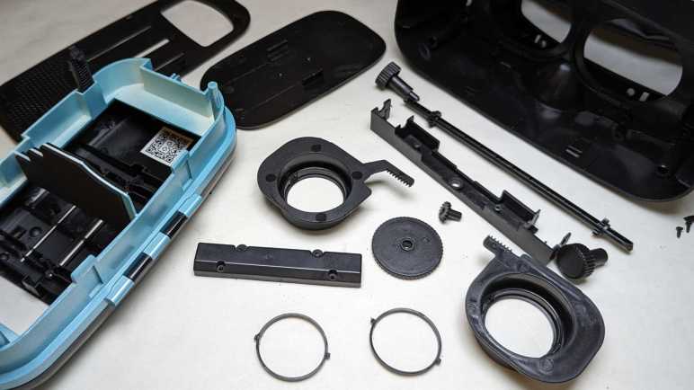
Implementation of focal distance adjustment is far simpler than Gear VR’s implementation, with a single axle rotating a pair of rack and pinion mechanisms. But this is a finicky thing that didn’t work as smoothly as Gear VR’s implementation.
Removing the center cover did not free the rotating axle: it is still held by either side.
But it did allow the axle to flex enough for me to pull off the front. I still couldn’t get to all of the remaining fasteners, though. The focal distance adjustment axle remained stubbornly in the way. My search for fasteners or retention mechanisms came up empty, I concluded it was glued in place.
Two snips with a diagonal cutter and the axle is no longer in my way. I could access all of the remaining fasteners now.
One set of fasteners held the rear of the headset in place.
The other set of fasteners held down the IPD adjustment mechanism: a single pinion gear moving the two eyepieces in opposite directions.
Both eyepieces were removed so I could salvage the lens, held by a retaining ring with two tabs.
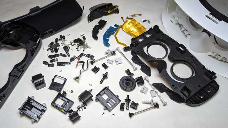
With the headset disassembled, I turn my attention to the controller. Which also looked great on the spec sheet but would frequently lose connection to my phone and felt cheaply made in the hand. (I suppose because it was.)
It runs off a pair of AAA batteries, which I forgot about and left them in this controller and now it is damaged from battery leakage. What matters today for disassembly is the pair of fasteners visible in the battery compartment.
The top piece came free easily, uncovering the button array and a two-axis joystick mounted on the mainboard’s top. A few screws held the mainboard in place.
Removing them freed the mainboard, so we can see the trigger switches board held by another pair of screws.
Removing the trigger button board for a closer look, I see a very straightforward implementation.
Mainboard backside. The biggest chip has the following markings:
This controller was easier to take apart than Google’s Daydream controller, with no glue holding things in. If it had a piece of weight like Daydream did it might feel more substantial in the hand, but that would not have improved the tactile feedback of its buttons.
Mechanically speaking, this headset was more complex than Daydream headset and simpler than Gear VR. Too bad it didn’t work as well as its spec sheet suggested. I think it’s because it tried to do too much. In contrast, Mattel View-Master VR keeps its feature scope constrained and does its job well.
While Google specified a handheld controller to their Daydream VR system, Samsung chose a different solution to Google Cardboard’s limited interactivity: they added controls to the side of their Gear VR headset. Reading that description, I thought they just added a single circuit board with a few buttons. The reality was far more mechanically complex, resulting in a far higher parts count than I had expected.
This is a Samsung Gear VR SM-R322, compatible with a half dozen Samsung devices including the Galaxy S7 phone. I bought this as a present for a friend who had a Galaxy S7. Years later, he retired that phone and donated it to my electronics tinkering. (After resetting and wiping his personal data, of course.) He also returned my present, still unopened.
Since Samsung has already shut down their Gear VR experiment, there wasn’t much I could do with it except to take it apart to see what’s inside. I plan to keep the lenses and nothing else.
Gear VR side controls are dominated by what looks like a four-direction pad but is actually a capacitive touchpad. Off to the side are physical tactile up/down buttons (feels like volume control?) and a back button.
An adjustment wheel at the top changes the distance between its lenses and the device screen. (Focal length.) I estimate its range of motion to be roughly one centimeter. Its implementation turned out to be more complex than I had expected.
The face gasket was held with hook-and-loop fasteners. Peeling it off didn’t reveal any fasteners or likely hiding places for them.
Pop off the front cover for a look the device holding mechanism.
Headset-to-device communication is done via this micro-USB plug, which can slide between two positions indicated by a green dot over either A or B. Most of device holding force is supplied between this clamp and its opposite number, which didn’t have a USB plug. Helping to keep the device in place are small bumpers at each corner.
A thin rubber pad adjacent to those bumpers hid fasteners, one for each corner. That hole next to the Philips-head screw is a part of the focal length adjustment mechanism.
Two additional fasteners were in the middle, hidden under a sticker.
Once undone, the device holder tray can be flipped open though it is still connected to the headset by this cable for USB connection and two of the side buttons. A flexible cable is required to bridge a gap whose size varies based on the focal length adjustment.
Freeing the USB cable required removing a cover to access all electrical connections to the mainboard.
Then the spring-loaded USB connector assembly could be freed and disassembled.
Looking inside the device holding tray, I realized the corner bumpers were more sophisticated than I had expected. I thought each corner was a single piece of squishy rubber, but it’s actually three distinct and individually spring-loaded piece of plastic. Multiply this out to all four corners and we end up with twelve sets of bumpers and springs.
Back to the headset main body, removing its mainboard allowed us to open it up to see the focal length adjustment mechanism.
Rotational motion from the top adjustment knob is transmitted via a series of gears and shafts to all four corners.
A close-up look at a corner mechanism translating rotational motion to linear motion.
Under the mainboard is a piece of black plastic that I had expected to host the capacitive touch pad, but it only had the back button. I can see four wires in this cable, which is double the amount I expected. A simple switch should only need two?
The capacitive touchpad is actually glued to the inside of the enclosure. Its control chip has the following markings:
The glue was tenacious and thus touchpad was damaged during removal. I don’t recall ever seeing this pattern in a capacitive touchpad before.
The final bit of electronics is a sensor that sits looking at the user’s forehead. Its location implies an optical proximity sensor to see if it is being held up to the user’s face.
The lens retention mechanism has three little clips that need a little push to release the lens.
There’s nothing fundamentally complex about adding side controls to a Google Cardboard-style headset. But when we add mechanisms to securely hold phones in a range of sizes plus the ability to adjust distance between lens and screen, we end up with a mechanically complex device with a high parts count. It worked really smoothly, though, perhaps all those parts were necessary for proper operation and going with a low part count design hurts functionality.
User interactivity in Google Cardboard was limited to a single button tapping anywhere on screen. Google decided to address that limitation with their follow up Daydream VR by adding the requirement of a handheld controller to go with the Daydream headset as a complete system.
The small text imprinted on the back of the controller included an FCC ID because this is a Bluetooth device operating over airwaves. Curiously, a search for A4R-D9SCA came up empty on the FCC ID search site. Looking around the internet for other resources, I found a teardown posted by SlashGear. I was disappointed (but not surprised) this device is largely glued together and will be more difficult than the headset to disassemble.
Fortunately, I have the freedom of not caring if I break it, so I started prying. Half of the controller (the palm end) was indeed held by glue. The other half (touchpad end) is designed to flex and so we can click the touchpad, thus it was only held by two clips that allowed a small range of motion.
Focusing on the top panel circuit board, I see a small white tactile button in the middle for clicking, and a chip with the following markings:
Curious what the other side looked like, I used my flush cutters to cut away melted plastic rivets holding the circuit board in place.
We see a grid of diamond-shaped metal pads for the IQS525 to sense our finger position.
The mainboard is held very securely. Not just by several screws, but also by glue. While the glue is brittle and easily cracked, it still put up quite a fight.
By the time I freed the mainboard, it was very bent.
Under that board is the battery and a small piece of metal that couldn’t be a heat sink as it doesn’t touch any of the chips. It’s probably just to add heft to the controller right in the middle of where our palm would be. It is mainly held by some double-sided tape, but it is also in contact with that glue. It takes a bit of effort to pry it free.
The battery is held by a stretch-release adhesive strip, but I have yet to develop the fine touch needed to make those strips work for me. I pulled too hard on this one and it broke. Fortunately, it released enough for the battery to come free. Aided by the fact the enclosure designed a bunch of ribs in the battery tray for a much smaller contact surface than if the enclosure had a smooth flat base. It’s curious we have these ribs and stretch-release adhesive features for easy battery removal, yet it is trapped under a circuit board that was glued in place. Some design criteria must have changed partway through development.
Since this small battery saw barely any actual use or much abuse during removal, I am willing to consider repurposing it in a future project.
Due to the copious amounts of adhesives and glue, this controller was annoying to take apart. In practice it is likely to be impossible to repair as well. The battery was far more difficult to remove than it really needed to be. I expect very few of them have been properly disposed or recycled after retirement.
I’ve decided to dispose all of my 3DoF VR headsets, which I haven’t touched since upgrading to 6DoF VR equipment. They will be taken apart to see how each manufacturer approaches building such a headset and extract their lenses for potential future projects. First up: a Google Daydream VR headset.
Daydream was Google’s effort to evolve from Cardboard. One major difference is the addition of a handheld controller. It has an accelerometer within for 3DoF tracking, a small round touchpad, and four buttons: two on the face and two on the side. Making it a required component means Daydream apps can take advantage of far more interactivity than Cardboard’s single tap.
Another evolution for user-friendliness were the two black nubs towards the center. They make contact with phone screen and register as two touch points. The Daydream app will read their position and adjust display image for proper alignment with the headset, using software smarts to eliminate one user headache. Pretty clever!
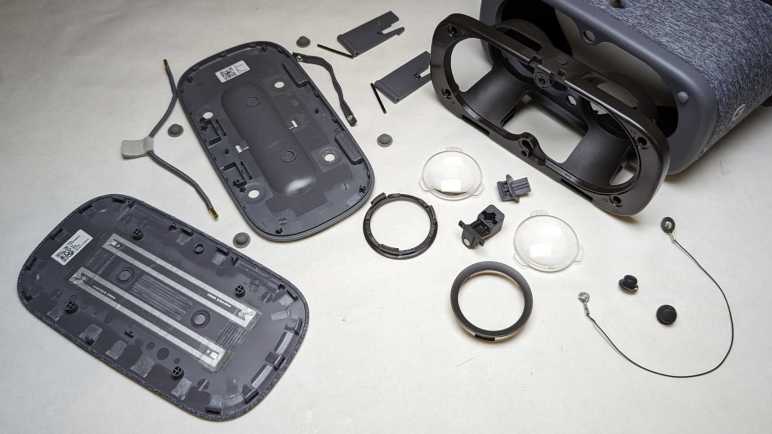
The easiest item to remove was the face gasket, held with hook-and-loop fasteners for cleaning or replacement.
Once removed, seven small Torx (T5) fasteners are accessible for removal.
The retaining mechanism for the front panel is also now accessible. To release them, disconnect the spring and press retaining hooks inward.
Front panel hinges can then be slid free.
I thought there might be fasteners underneath rubber nubs in the front panel. I was wrong.
Brute force prying released the extensive set of plastic clips holding two halves together. Not all of the clips survived this process.
Once those two halves were separated, everything else inside the panel came away freely. Hinge pins, elastic holding straps, etc.
As soon as the phone was inserted into this Daydream headset, it knew to go to Google Play store and download the appropriate Google app. (Another user-friendliness advancement.) I wondered how that was accomplished and the answer are these RFID strips made by Identiv.
Back to the headset, there was one more Torx fastener hiding in a different place and orientation from all the others, up near the top of our nose.
Its removal frees the hook at the top of the headset.
Which then frees up the optical frame. I was surprised to see a length of wire for electrically connecting the two screen alignment nubs.
I’ll keep the wire — and the two nubs — in case I want to play with capacitive touchscreens.
The lenses are clipped in at three points with a simple mechanism.
Tearing down a relatively simple AR beacon was the final step (after the headset and the lightsaber) of dismantling Lenovo’s disappointingStar Wars: Jedi Challenges game for disposal. Since I was still in a teardown mood, I decided to continue dismantling my collection of phone-based headsets. I have quite a collection and, in hindsight, they’ve all been money wasted. Those devices could only react to motion in three degrees of freedom and never approached the immersion of real VR headsets that can track six degrees of freedom. I packed them away after getting my first 6DoF headset, thinking I might find a way to do something creative with the phone-based headsets.
I never got around to devising interesting projects with Google Cardboard (and derivatives) and it’s not going to get any easier in the future. Google officially killed Cardboard in 2021, but by then it was merely a formality. Derivatives (and wannabe successors) like Samsung Gear VR and Google Daydream were abandoned even earlier. With official support discontinued, software support for any potential project ideas also faded away. The first-party SDKs have either gone stale or have disappeared. Third-party support is no better, being removed from tools like Unity and Unreal. And finally, infrastructure support like Samsung Gear VR Store and Google Daydream app have been taken offline. If I want to write code for Google Cardboard/Daydream/Gear VR I would almost have to work on my own scratch, like another long-past-its-prime hardware platform Windows Phone. But this would actually be even more difficult, because I don’t know how to work with these lenses in software in terms of 3D rendering projection math.
Therefore, using them as VR headsets would require more effort than I’m likely to spend. Keeping them intact as VR headsets consume a lot of space with no good payoff I can foresee. Looking at this very simple design, the only reuse possibility I can imagine are those lenses in a non-VR application. At the very least, a bag of salvaged lenses would occupy less space than a bag of obsolete and abandoned VR headsets. With this line of thinking, my phone-based VR headset purge begins. First on the workbench: Google Daydream VR Headset.
A shiny plastic “lightsaber” is the main peripheral of Star Wars: Jedi Challenges and it was fun to take apart. There was another peripheral in the box, a glowing ball beacon to support certain scenarios.
In this beacon’s base is a three-position switch. Center position is off, and moving to either side would illuminate the soft white translucent sphere. One position gives us cyan, the other position magenta. Given this behavior, I guessed the lowest-cost implementation would be a strictly analog system with LEDs connected to a resistor network. Time to open it up and see if my guess is correct.
This beacon uses AA batteries instead of lithium-ion rechargeable.
Product labels live in the AA battery tray.
Unlike the lightsaber, there is no FCC ID here meaning it doesn’t communicate with the phone or the lightsaber over radio waves. There is no USB port or any other hardwired communication. There might possibly be some kind of communication via lights or sound.
Two Philips-head fasteners live under those stickers. Remove those stickers, then two screws, followed by a few plastic clips to separate top and bottom halves.
Wow, my guess of “a few LEDs and a few resistors” was very wrong. This is a surprisingly complex mainboard. I’ve already ruled out radio wave or hardwired data communication. Looking on the board, I couldn’t find anything I recognized as a light sensor for optical communication or a microphone/speaker for audio communication. If this is completely passive, why all this hardware?
Instead of a cyan LED and a magenta LED, in the middle was a full RGB LED capable of arbitrary colors. The surface mount component itself appears identical to the unit illuminating the tip of the lightsaber. Full color capability is not a huge surprise in itself. But in the absence of external communication, how would it know to display another color?
I can see the following markings on the chip in the corner:
S033
PHVG
725Y
Searching on these designations, my first hit was a question about an electronic cigarette. I know nothing about vaping hardware, but I had not expected them to require microcontroller smarts, either. (I’m surprised twice within a short span.) The chip was identified as the STM8S003F3 and a look in its datasheet confirmed the device marking for UFQFPN20 packaging has a first line of S033 matching what I see here.
The STM8S003F3 is a relatively simple 8-bit microcontroller with eight kilobytes of flash program storage and a single kilobyte of working memory. These are modest specs, a fraction of the ATmega328P at the heart of an Arduino Uno, but it is still overkill for a device that just shines a LED in one of two colors.
This beacon must be capable of far more than what I’ve seen it do. Which is highly likely, given my short time spent actually playing Star Wars: Jedi Challenges. But looking at the hardware in front of me here, I don’t see how it could interact with the rest of the system to unleash said capability. Still, it was an interesting look inside. I’m enjoying this particular streak of teardowns so I will continue with the rest of my phone-based headsets.
I was disappointed by Star Wars: Jedi Challenges as a product, thankful I only paid clearance price for it but that also meant I couldn’t demand a refund for a lackluster experience. No matter, I still got enjoyment by taking apart its Lenovo Mirage AR headset to learn how it worked. And now I will take apart the main peripheral: Rey’s Lightsaber.
Production promotion proclaimed this to be a “collectible-grade” lightsaber. I have no idea what that is supposed to mean. Perhaps Disney licensing department has defined categories for their merchandise, but as far as I’m concerned, it’s just marketing fluff.
Fluff aside, I will give it credit for being far more detailed than I had expected. A high-quality shiny chrome finish throughout the device gave it a much more premium look than cheap Halloween costume lightsabers made out of dull gray plastic pretending to be metal. Chrome finish aside, though, this is sadly still just plastic pretending to be metal.
This saber talks to the phone inside the Mirage AR headset via Bluetooth. (When powered on, my phone can see it as a Bluetooth device named “Rey’s Saber”.) FCC paperwork is required for all consumer products sold in the United States that transmit and receive data over any kind of radio frequency including Bluetooth. Such data is public record so armed with an FCC ID (O57AR7651N in this case: O57 is Lenovo, and AR7651N is the Jedi Challenges product) we can go to FCC’s ID search page and see what has been filed for a product. This frequently includes photos of the product in disassembled form, a very useful guide for teardowns. Nothing like a detailed iFixit teardown guide, but we can see the major pieces and look for fastener locations. It cuts down on the fruitless hunting, especially when the fasteners are well hidden, which they were for this saber.
Thanks to the filing document “TempConfidential_Internal Photos_Rev1” PDF, I could see a fastener lined up exactly at the location of a nonfunctional button. It was held with double-sided tape and could be removed to access the Philips-head screw underneath.
Freeing that single screwed allowed the tip to slide out.
If somebody wanted to repurpose this lightsaber as a costume prop, it should be easy to replace the soft translucent white tip with something more appropriately mechanical in appearance.
That translucent white tip is illuminated by this surface mount component.
Backside of this small circuit board indicates it is a trio of LEDs in a single surface mount package, controlled by four wires: one each for green, red, and blue and a common ground.
Returning to the FCC filing PDF, I saw the base had two heat-set inserts to accommodate machine screws and the picture quickly guided me to where they were hidden underneath glued-on rubber pads.
Remove those two to release the base.
Rubber pads hid two more screws.
Removing them allowed the grip to slide off.
Things got trickier from here. Looking at filing pictures I could see a screw is hidden underneath this button, but I couldn’t see a graceful way to access it.
I ended up prying against the four little claws inside the saber in order to release the button, then I could access that screw.
Then I could slide off the center ring section, exposing three final screws holding the exterior in place. Once removed the exterior could slide a fraction of a millimeter but it is not yet completely freed.
A bit of wiggling pointed to this button as the culprit. This is a functional button and that knurled surround hints at a ring I could remove, but that was an illusion. I saw little plastic pieces inside and thought I should pry them free just like I did the previous button.
That was a mistake. Prying the button free damaged both it and the socket it resided in. Now that I could look at its distorted shape, it appears to be designed to be uninstalled with a quarter-turn counterclockwise. I have no idea how I would grip this button (while installed) solidly enough to perform that quarter turn overcoming the little nub designed to resist accidental turning. Maybe a suction cup? I don’t know. What I do know is that it’s now too damaged to be reinstalled with a quarter turn clockwise. I had hoped to tear down this saber nondestructively in case I have an idea for repurposing it, but I have passed that point of no return. Ah well.
Setting that disappointment aside, I can look at saber internals. It is a very thinly populated board with few components.
The black plastic backbone securely holds an electric motor with an eccentric weight on its shaft. This would be good for shaking the saber in our hands to signify battle action.
The black plastic frame also holds this piece of metal that does nothing except add heft to the saber so it feels appropriately substantial when picked up.
Given its weight, I had expected a chunky array of NiMH or even NiCad rechargeable batteries inside, but it’s actually a slab of metal and this thin little lithium-polymer pouch. I would have said it was undersized to drive the tactile feedback motor but I’m no battery engineer.
Several test points are visible adjacent to the battery directly behind the microcontroller. I assume Lenovo/Disney locked down the nRF52832 so we can’t flash our own firmware. Maybe a skilled ARM security researcher could find a way in via glitching the power supply for fault injection, but I don’t know how to do that. The locked-down nRF52832 can be unsoldered and replaced with an unlocked chip, but such tiny BGA chips are also beyond my current skill level.
I didn’t expect to find much in the way of reusable components, and I didn’t. I was surprised at the robustness of the mechanical construction. I had expected to find a single screw and have it fall apart in two halves. I’m glad I found the FCC filing PDF, which made this teardown go smoother and almost nondestructively. Now for a change of pace, I’ll take apart the final hardware component of Star Wars: Jedi Challenges, a simple illuminated AR beacon.
The Lenovo Mirage AR Headset (bundled with Star Wars: Jedi Challenges) was a huge disappointment, now I’m going to extract what entertainment I can from tearing it down. From a mechanical engineering perspective, I was very impressed by what I saw. Unfortunately, robust mechanical design could not overcome fundamental product weaknesses.
Before I started the teardown, though, I was curious how it would enumerate as a USB device. I plugged it into a computer running Ubuntu and here’s what got dumped out via dmesg:
usb 3-1: new full-speed USB device number 3 using xhci_hcd
usb 3-1: New USB device found, idVendor=1f3b, idProduct=1000, bcdDevice= 2.00
usb 3-1: New USB device strings: Mfr=1, Product=2, SerialNumber=3
usb 3-1: Product: AR Head Mounted Device
usb 3-1: Manufacturer: Lenovo
usb 3-1: SerialNumber: 101215-0073
hid: raw HID events driver (C) Jiri Kosina
usbcore: registered new interface driver usbhid
usbhid: USB HID core driver
hid-generic 0003:1F3B:1000.0001: hiddev1,hidraw0: USB HID v1.11 Device [Lenovo AR Head Mounted Device] on usb-0000:00:14.0-1/input0
Looks like it conforms to USB HID standards, but as a “raw” device not obligated to conform to any common peripheral. Since it doesn’t try to pretend to be something common (say, a mouse) we have to know its raw USB communication format in order to communicate with this device. If I still had the app installed on my phone, I could peek at its control schema using a USB reverse engineering tool like Cynthion (formerly LUNA). But I had neither. With my skill level and what I have on hand, I can’t do much except take it apart.
I started with the easiest removal: the head strap which was held by hook-and-loop fasteners.
Next was the phone caddy, the only other user-removable part in this system. Visible in this picture is the short USB cable for the headset electronics to communicate with the phone. I used this headset with a Google Pixel so this is the USB-C cable. The headset came with two other cables: micro-B for other Android phones, and a Lightning for Apple iPhones.
The caddy had to accommodate over a dozen different phones and thus had mechanisms to adjust for different width, height, and thickness.
Working to meet those requirements were a lot of intricate details in the design of these injection-molded parts. (Aided by a few inserts made of stamped sheet metal.)
Next to the caddy slot (and USB port) is a product information sticker.
Reaching the end of user-serviceable parts, I pulled out my iFixit Mako screwdriver kit and started removing fasteners visible on the bottom. (Center fastener was hidden under a sticker.) There were multiple different lengths of fasteners. Some were machine screws and some self-tap into plastic. But with one minor exception, I only needed a single screwdriver bit to drive them all. That must have been a conscientious decision by the mechanical engineering team and I appreciate their effort.
First plastic piece to be removed was the clear front piece, whose removal exposed several more fasteners.
Fasteners were also hidden under dark plastics on the sides, though these wouldn’t be important until a little later.
After removing every fastener I could find, the headset remains stubbornly sturdy. Flexing it in my hands failed to highlight any promising seams to pry against, so I started prying at every seam between different materials. The first clips to release were next to the side buttons.
Following those clips around the perimeter allowed the top to be released and unveil a circuit board and a battery. The circuit board is labeled with Legend_HMD_MB_PCB_V05 2017.08.10. I interpret this to mean: Legend = project code name, HMD = head-mounted display,. MB = motherboard, PCB = printed circuit board, V05 = fifth revision. Followed by date of August 10th, 2017.
Biggest chip on the circuit board is an STM32F205RE microcontroller, built around an ARM Cortex-M3. The next biggest chip is a LFE5U-45F 6MG285C Lattice Semiconductor FPGA. I assume the camera-based object tracking algorithm is implemented in this FPGA. I couldn’t find that specific part number on Lattice web site, perhaps it is an obsolete part? I was redirected to the page for Lattice ECP5 family so I guess it’s one of those. Most of the left third of this board is unpopulated, with footprint for at least one nontrivial BGA part. I wonder what they had planned for that area? That is near the trio of side buttons, perhaps they had plans for other headset designs with different side controls? One possibility is a touchpad and if so that BGA footprint might be a capacitive touch processor.
The bottom of the phone tray caddy area turned out to be a sticker I needed to peel off in order to expose more fasteners.
Once released, we could remove the louvered bottom as well as dark smoke colored side pieces.
Optical reflector assembly fasteners are now accessible.
The optical reflector assembly (laying upside-down in this picture) consisted of three pieces of clear plastic with semi-reflective coatings. One flat sheet spans the entire width, and two curved half-width pieces one for each eye. Looking at the geometry, I now understand how this works and I’m not impressed. I don’t know how much light the coating reflects and how much is transmitted, but using 50% as an example, this is what we would end up with:
Image from phone screen shines down to the flat sheet. 50% of the light is transmitted straight through and lost out the louvers in the bottom of the headset.
The remaining 50% is reflected to the two curved pieces. Of that original 50%, 25% is transmitted through and forwards, lost to the environment. The remaining 25% of that original light is reflected back towards the flat sheet.
The flat sheet reflects 12.5% of original light right back into the phone, where we can’t see it.
That leaves 12.5% of original phone screen light transmitted through the flat sheet into our eyes.
Only a small fraction of light makes it all the way to our eyes, no wonder everything was so dim! This reflector assembly is part of a recurring theme: it is mechanically sound with sturdy mounting, but robust mechanical engineering could not overcome a fundamentally inefficient optical path design.
Now that I understand how it works, I’m not terribly interested in keeping this optical assembly for homebrew AR headset adventures. Also, for accurate projection I need to know the curvature of those two half-width pieces and I don’t have that data. Reverse engineering that information takes knowledge of optics that I currently lack. Can I do something with this (or pieces of it) with the skills I have now? I’ll set this reflector assembly aside for a little bit longer while I think.
Resuming the teardown, I couldn’t find any fasteners holding down plastic pieces surrounding the camera. A little exploratory prying popped them loose: they were held with double-side tape.
Now I could remove the camera assembly. Two cameras are held at a precise distance apart by a metal frame, the only metal structure in the entire headset. Metal rigidity would be useful to maintain distance, but it also serves as heat sink for the pair of cameras.
A trio of Philips-head fasteners hold the camera to the frame. I had hoped for some identifying marks on the back of these cameras, but no luck. The only markers were on the thin ribbon cable. A QR code that scanned out to 8SSC28C19780AXYY7A55567 (no clue) and human readable text as follows:
MDG001-200
SUNNY
B1734
94V-0
2PE
E310562
Searching the web for that information, I learned 94V-0 is an UL standard for flame resistance and probably refers to the FPC (flexible printed circuit) substrate. “Sunny” probably refers to Sunny Optical, a Chinese company for camera modules. Lots of camera modules are listed on their website but I didn’t find a match for any of these numbers. The site had a section for VR/AR products, but the only listing is for an eyepiece lens. Sunny E310562 got a few hits on eBay for camera modules corresponding to other Lenovo products, which makes me feel like I’m on the right track, but they look very different. Not sure what’s going on there. I think I struck out.
The lens is removable. I don’t know enough about small cameras to recognize if it this was a standardized lens mount form factor or something proprietary. I removed the lens hoping to see some identifying markers inside. I saw the imaging sensor array, but no identifiers. This camera was significantly larger than OV2640 popular with electronics hobbyist kits and much larger than what I’ve pulled from phones and tablets. I expect this to be a very capable camera and it’s a shame I can’t repurpose it for robot vision or something.
That was a fun teardown and I learned more than I had expected, including an understanding of this optical reflector’s fundamentally flawed design. But I’m not done yet: this is part of Star Wars: Jedi Challenges and a Jedi needs a lightsaber.
Headphone jacks are disappearing from recent phones, which is a shame. Thanks to global volume, wired earbuds have become simple and effective accessories for audio on-the-go. So inexpensive as to be practically disposable, the price fits with the fact they have a finite and short lifespan. As the wires flex and bend, they eventually break and cause intermittent connections audible as cracks and pops. Which was why this particular set (Monoprice #18591) was retired.
Compact and lightweight, there’s hardly any material here at all to reclaim or recycle. But there’s a small rare earth magnet inside each earbud, and I want to extract them before the remaining carcass heads to the landfill. Similar to what I did to a retired iPad cover case.
These earbuds had been waiting processing for a while, hence the dust.
The soft rubber layer pops off easily. As I recall this was a user-replaceable item. The earbuds came with three sizes. The midsize one is installed by default, with smaller and larger sizes in the package the user can switch to best match the size of their ear canal.
There were no further user-serviceable parts. Everything else is molded or glued together so I had to break things apart with a pair of pliers.
Inside the black plastic enclosure is a shiny metal case for the tiny soundmaker.
Prying off the front metal plate exposes the thin membrane that vibrates with a small copper coil. Inside the center of that copper coil is the magnet I seek.
The magnet is glued to the enclosure, but thankfully the glue here wasn’t very strong. Bending the sheet metal to get more clearance, I was able to reach in with a thin metal tool and pop out the magnet.
Attached to the magnet is a thin metal circle of the same diameter. I think it serves as a spacer, held on by the same not-very-strong glue so I could separate it from the magnet.
Here’s the entire stack disassembled. Circled in red square is the magnet I will keep. Remainder will head to landfill.
I enjoyed exploring leading edge web development with experimental features like magnetometer API and evolving standards like PWA. But learning about the trailing edge also has some value for me. I have a stack of old Windows Phone 8 devices. Microsoft had shut down native app development for the platform as part of its end-of-life treatment, leaving its onboard web browser as the only remaining entry point. Based on Internet Explorer 11, support of which has been dropping from platforms left and right, there’s definitely a clock ticking away if I want to be able to do anything with those phones.
Assuming, of course, those phones don’t decay and die on their own like this Nokia Lumia 520 has done. It’s been a guinea pig to test things like ESA’s ISS tracker web app. When I turned it on recently, it failed to boot and crashed to this blue screen of death. Unlike its desktop Windows equivalent, there are no debug information printed onscreen. Documentation has been purged from Microsoft and Nokia websites as they have disowned these devices. So, it was up to iFixit to preserve documentation on performing factory reset with a hardware key sequence: From powered off state, hold [volume down] and press [power] to start phone. As soon as phone vibrates, release [power]. Once phone boots to exclamation mark, release [volume down]. Press key sequence [volume up], [volume down], [power], [volume down]. Watch spinning gear onscreen for a few minutes.
But performing such a reset on this phone didn’t help, I just ended back at the sad faced blue screen of death. I don’t know what happened to this phone. I hadn’t thought electronics would decay with time, but something on this one has failed in a way I lacked information or tools to diagnose. I powered up my remaining Windows Phones and they were able to boot, so it’s not a common/widespread failure mode. (Yet?) In any case, today this dead phone gets the teardown treatment.
Nokia Lumia 520 was a simple and basic entry-level phone, dating back to the era when batteries were easily accessible and removable by the user. Not so much anymore, which is sad though there are occasional encouraging signs. Popping off the easily-removed blue back cover, we see physical features like a microSD card slot, SIM slot, and headphone jack. All useful features disappearing from modern phones.
The next layer is a black plastic cover held by multiple Torx fasteners and plastic clips. Removing that cover exposes phone mainboard, where we can see the thickest component is the rear-facing camera. It actually sits in the middle of a hole cut out of the circuit board, protruding both in front and behind of the board. (Lumia 520 does not have a front-facing camera.)
Ribbon cable near the top of the device is for touch digitizer input via this Synaptics chip.
Synaptics
S22028
33120155
ACAN310
Sadly, a web search with engraved text failed to return anything useful.
The touch controller communicated with the rest of the phone with ten wires, but they are far too fine-pitched for my current skill level to work with.
It’s a similar story with the LCD, connected to mainboard with twenty wires. Far too few to directly control an 800x480x3 LCD array, these must be data buses communicating with a controller somewhere downstream. At least six of these wires visibly hint at differential signal pairs.
Front and back views of removed mainboard. Full of tiny components, most of which hidden under RF shields, I see only two components (battery connector and vibration motor) that I could realistically repurpose.
With mainboard removed, I see no further fasteners to remove, and no obvious seams.
I knew it was too complex to be a single piece, so I manually twisted the assembly looking for signs of seams between parts. Attacking candidates with iFixit picks allowed me to separate the front panel touch digitizer from display subassembly.
The display assembly is held to its chassis frame with a few strips of adhesives and could be carefully peeled apart.
Freed from its structural frame, the display assembly feels very delicate. It easily flexes and twists to reveal details like these side-emitting LEDs for backlight illumination.
Peeling back foil tape uncovered ultra fine-pitched LCD array control wires embedded between layers of glass.
Trying to separate LCD array from backlight, I unfortunately cracked the glass and destroyed the LCD. I might be able to reuse the LED backlight but it’s going to be a serious challenge finding (and soldering to) those fine wires for LED power.
Goodbye, Nokia Lumia 520. I’m sad I didn’t get around to finding something interesting to reuse you as a whole unit. And your component parts are mostly too tiny for my current skill level to work with. But your death gave me a kick in the pants to get on with my studies. I hope to make use of your surviving contemporaries.
This Christmas themed novelty product “Snowglobe Orange & Gingerbread Gin Liqueur” is an alcohol beverage packaged in a globular glass bottle resembling a snow globe. Contributing to the theme is a small quantity of edible gold flakes in the liquid that can float like snowflakes, illuminated by LEDs embedded in the base. I didn’t care about the alcohol, but I asked (and was given) the empty bottle afterwards so I could remove that LED circuit to see an example of low-cost disposable production.
Each press of the bottom toggles LED power on/off. There may be a sleep timer to turn off LED after some period, but I didn’t test that.
The LED circuit board is surrounded by a circle of soft foam, which is in turn glued to the bottle. It peeled off easily.
Four surface-mounted white LEDs are visible, labeled L1 through L4. Each pair (L1+L2, L3+L4) are in series. The two 3V coin-cell batteries are also in series for 6V power supply. Battery positive terminal is connected to both pairs of LED series at their anode (+) and control chip U1. Battery ground is connected to control chip U1 and nowhere else. U1 has six pins: two pins for power and ground, two for LED cathode (one for each pair), and two more for the switch.
Peeling circuit board away from foam, the two switch terminals are visible. Closing this circuit is the job of a small piece of conductive metal, here still held by the bottom sticker. The metal is a thin springy sheet stamped into a dome shape. Pressing and collapsing the dome closes the switch circuit. Releasing the dome lets it pop back up and open the circuit.
Anything that conducts electricity bridged across those circuit board contacts will toggle LED on/off.
This was designed to be thrown away along with the bottle once the alcohol has been consumed. I’ve tossed the bottle into glass recycle bin and I’m keeping the light, even though at the moment I have no use for a dim battery-powered LED circuit with push on/off.
Using a brushed DC motors is easy: apply voltage, watch motor shaft turn. I’m exploring brushless DC motors and even the cheapest controller from Amazon had features that I hadn’t even known existed. It is far more sophisticated than a DC motor driver (DRV8833) I explored earlier. To make it actually turn a motor, I’ll start simple with the smallest brushless motor I found in my pile of salvaged hardware.
This is a small brushless motor in the spindle of a CD or DVD drive. Based on the fact it is only a few millimeters thick, it was probably salvaged from a laptop optical drive. Lots of wires visible in the pale-yellow ribbon cable. I will need to probe them looking for a set of three or four wires, with a tiny bit of resistance between them, that would indicate coils for the brushless motor.
I probed the set of four contacts closest to the motor, but found no electrical connection between them.
This set of four wires looked promising. They ended abruptly, as if I had cut them off from a larger piece of pale yellow flexible printed circuit. (FPC) I guess the rest of that circuit didn’t look interesting to keep and what they were have been lost to history. I used sandpaper to uncover the copper traces within this cut-off segment. This work was for naught: no electrical connections here either.
This left the large connector of many wires. I noticed the five conductors in the middle are wider than the rest. Each of those led to two contact points on the connector. I started with those and found likely candidates in three of the five wide wires. I’m not sure what the other two were… perhaps power and ground for some other circuit? Whatever they were, I hope they aren’t relevant to my current experiment.
I soldered thin (30 gauge *) wires to each of those points. Using an old AA battery as ~1V source, energizing any two of these wires would result in the motor holding a position. Motor coils confirmed!
A bit of careful cutting and heat-shrink tubing isolated these wires from each other.
After taking apart a hard drive that went to great lengths to be just 5mm thick, I moved on to an SSD whose circuit board of surface-mounted chips were even thinner without even trying. This Intel 320 Series SSD should still be usable today, but it isn’t because of an overzealous security feature.
My Dell Inspiron 15 7577 came with a secure data wipe feature in BIOS and I decided to use it to securely wipe data from this SSD. What was critically missing from its description was that, as part of securing my data, this feature would lock the drive with a password that is never displayed. (“Lock it up and throw away the key.”) This fulfilled the task of securing any data on the SSD, but it made it impossible to reuse the SSD elsewhere. This 300GB capacity SSD cost over $500 in 2012, so I was NOT HAPPY it was rendered unusable. At the time Dell claimed the security feature was Working By Design. Later on, it admitted the behavior was a bug after all and offered BIOS updates to some other computers (not mine) to remove this behavior. Doesn’t matter, I’ve learned my lesson and never used the feature again.
I hung on to this unusable SSD for years, hoping to find a utility that could somehow reset the device and unlock the capacity that Dell overzealously locked away. But now, with new 500GB SSDs available for less than $50, I finally conceded there’s no point.
The thick black plastic shim brought it to 9mm height typical of laptop HDDs but can be removed to fit in spaces designed for thinner 7mm HDDs. It looks bulky next to the 5mm thick WD5000M21K hybrid drive, but that was merely a metal enclosure.
Once removed from its enclosure, we can see an internal circuit board who is barely 3mm thick not counting the SATA connector.
The brain in charge of this operation is Intel’s own PC29AS21BA0 controller.
Data is stored across 20 Intel 29F16B08CCMEI flash memory chips, 10 on the front side and 10 on the back. I hypothesize they are each good for 16GB of raw storage. 20 of them together would give 320GB of raw storage, 300 of which is accessible to user and 20 reserved for SSD housekeeping.
Hynix H55S5162EFA is probably a bit of dynamic memory used by the controller chip to do its job. Intel sold its flash memory division to Hynix, so technically speaking this entire device is now Hynix.
The whole point of secure data wipe (and lock) is to render all data safely inaccessible, so I should be good to stop. But why pass up a chance to play? Just like my previous decommissioned SSD, I’m going to remove those flash chips with my paint-stripping hot air gun. This blunt tool is unsuitable for electronics work if we want delicate devices to work again. But in this case, if the heat should damage a chip beyond repair, that would be a feature and not a bug.
A few minutes later, I had a loose jumble of flash memory and other chips. Even if the heat gun hasn’t destroyed the chips completely, anyone who wants to steal my data will need to figure out which chip went in which location. (I recommend they find a different hobby.)
For contrast with the old Toshiba laptop hard drive I just took apart, I decided to follow up with this Western Digital WD5000M21K. This is a hybrid device with both a spinning magnetic platter and flash memory solid-state storage. In theory it is the best of both worlds offering large-capacity (500GB) storage and solid-state drive performance for cached data, all packed in an impressively compact SFF-8784 form factor. It is only 5mm thick! The mechanical engineers must have been fighting for fractions of millimeters designing its innards.
In practice, its performance was abysmal. It was nowhere near SSD level and felt even worse than contemporary HDDs. Its performance was utterly blown away by a M.2 SATA SSD (in an SFF-8784 adapter card) which, because they were just small circuit boards, were effortlessly more compact on top of better performance. Dropping SSD prices have eliminated the niche of compact mechanical hybrid drives. Ending this line of evolution to sit alongside VHS+DVD players in history as transitionary products with a limited shelf life.
One thing that caught my attention was a sticker covering the entire top surface of this device, and it wasn’t even very densely printed with information. As I would learn later, this sticker is not merely cosmetic.
Most product information was actually printed on a sticker on the other side of the device, surrounding the motor where we can see three wires implying a delta style winding. This drive’s control board is much smaller than the older Toshiba drive, even though it had to include a SanDisk-branded chip providing its 8GB of flash memory (“SSD”) cache. Its size was helped by the compact SFF-8784 style connector. A standard SATA connector would have required almost half of the volume of this entire control board.
Returning to the top side, I removed the sticker and saw why it covered everything: it’s a part of this drive’s airtight seal. WIth top sticker gone, an ~1mm gap surrounding the voice coil magnet assembly is now open to outside air.
Most of the Torx fasteners were T2, except for the one at the center of the platter which is even smaller. I assume it is a T1, but I don’t know for sure as I don’t have a driver. I’m using iFixit’s Mako Driver Kit and the smallest Torx bit is a T2. Not even their larger Manta kit has a T1.
Of course, that’s not going to stop me. As I’m not worried about putting it back together, or metal particle contamination, I have the option of drilling off the tiny screw head today. I might not always have that option, though, so to be prepared I found and ordered a driver set (*) because it claimed to include T1.
Once drilled out, I could remove the thin metal top lid and saw a single platter within. (I would have been astounded if they could pack multiple platters in here.) It has a an off-platter parking spot very similar to the Toshiba laptop drive, but it doesn’t have the mystery latch mechanism. After that point I was pretty stuck. I could not figure out how to free the bearing from the voice coil arm. I could not find a way to disassemble that stack. And I could not figure out how to free the platters. For the platters, it appears I need a special wrench that engages with the eight dimples on the spindle and use it as leverage to turn against the four surrounding slots.
As an amusing size comparison, here’s the compact WD5000M21K next to the spindle motor assembly from a 3.5″ sized WD800 hard drive. It’s an impressive feat of engineering, packing all these mechanical components within 5mm of thickness. But technology moves on, and SSDs are far thinner by nature.
(*) Disclosure: As an Amazon Associate I earn from qualifying purchases.
Removing a rather large sticker label unveiled just one hidden screw.
After removing those screws, the lid came off easily.
I was surprised to find two platters was packed in this drive less than a centimeter thick representative impressive miniaturization at work. One difference between a desktop drive and this laptop drive is the read-write heads are physically pulled off the platter in parked position. I was under the impression HDD read-write heads are far too fragile for transition a gap between mechanical pieces or rubbing against anything other than a cushion of air. Seeing this tells me they’re not as fragile as I had thought, but I don’t know what the actual engineering constraints involved.
On the opposite end of the pivot, beyond the voice coil actuator, is this mechanism whose purpose I don’t fully understand. The pivoting metal arm could slot into a sharp hook next to the voice coil, keeping the read-write head away from the platter. But how does it know when to engage or not? It works in conjunction with the white plastic part, but I couldn’t figure out how the whole mechanism works together. My best guess is that we have a clever mechanism that would lock the pivot safely in place until the voice coil actuated pivot performs effectively a “secret knock.” Taking advantage of inertia and momentum, the right sequence of motion would release the lock. To verify this hypothesis, I would need to reassemble the drive and see if I can power it up, but by the time I thought of doing so, I had already passed the point of no return.
Because with the mystery latch removed, it was easy to remove the read-write head assembly and once I did, I could not put it back into place.
Flipping it over, I see a hex nut holding the entire stack together.
Loosening and removing the nut allowed disassembly of the entire stack.
I was surprised to find both platters were held by a single screw. Platters for large desktop drives always had multiple fasteners to ensure their platters could not rotate out of place. With a single screw, we don’t have that mechanical guarantee. I guess it’s just friction preventing these platters from rotating relative to each other or the spindle.
I was pretty impressed at how thin and compact this laptop hard drive was, but hard drive engineers have done even better than this.
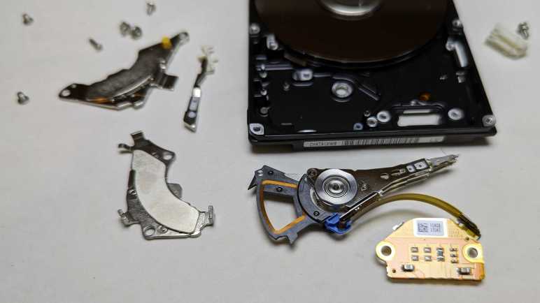
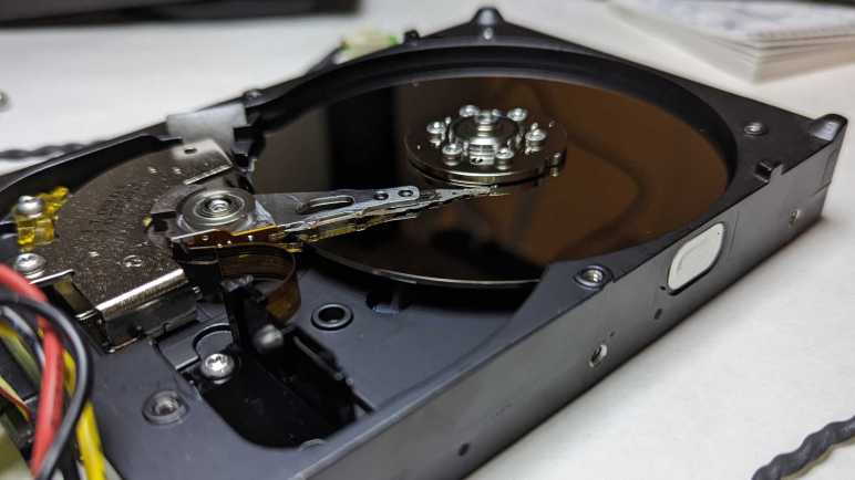
I’ve taken apart countless numbers of 3.5″ desktop hard drives like a Western Digital WD800, but I haven’t taken apart many (any?) 2.5″ laptop drives. There used to be a significant price premium for laptop components, an extra cost that I didn’t need to pay for my own needs. This started changing a few years ago: increasing power efficiency requirements and benefits of miniaturization meant small and power efficient components no longer demand a huge price increase, and nowadays laptops outsell desktops. Also, dropping prices of flash memory solid-state drives meant a lot of laptop-sized 2.5″ hard drives got replaced. With terabyte SSDs available for well under a hundred bucks, I can’t think of any reason why I’d ever want to use a 250GB laptop sized hard drive again, so I’m taking apart this Toshiba HDD2D90.
On the bottom I see four wires going into the spindle motor, which I now know to be a brushless motor with “Wye” style winding.
Closest to the motor control contacts is a chip with Texas Instruments logo and text 7CCN5NTA G4 TLS2502.
Chip with largest surface area was set at an angle relative to everything else. I don’t recognize the logo offhand, but a brief search with PSC acronym found Taiwan-based Powerchip Semiconductor Corp and a matching logo. I didn’t find an exact match for text A2V64S40CTP 747AFD1N but similar model numbers designated memory chips.
Spansion was acquired by Cypress Semiconductor which was itself acquired by Infineon Technologies. After multiple mergers, it was pretty hopeless trying to find details on a FL040A005 74699043. But Spansion’s main product line were flash memory, so this is probably a chunk of flash holding configuration, calibration, and drive-specific information such as remapping of bad blocks.
In between the DRAM candidate and flash memory candidate is a large chip with an old Marvell logo and text 8816717-TFJ1 FT15241.2 0747 C0P TW
My failure to find much of any information on the above chips were disappointing, but at this point no longer surprising. I continued onward to mechanical disassembly.
I looked over the control circuit board for a Western Digital WD800 hard drive and failed to find any documentation relating to chips I found onboard. Oh well. Maybe I’ll have better luck with another drive. For this drive, I continue on to familiar territory: take it apart to marvel at all those mechanical wonders within. As a side effect, this will also make all data stored on this drive functionally inaccessible.
The only tricky part with disassembly is that two of the Torx screws holding lid in place were hidden under the label sticker.
Inside we see a single platter. I’m pretty sure 2002 was recent enough for multi-platter drives, which would mean 80GB was not the highest capacity model in this product line even when it was new.
A translucent yellow bracket limits possible range of motion with read-write head. A small magnet is embedded on one end, but I don’t know its design intent. Perhaps it held the head in place when there’s no power? This bracket is held by a single screw and had to be removed before the read-write head can pivot far enough to clear the platter.
Visible in this picture under the read-write head voice coil is one of two very powerful magnets buried inside this hard drive, the other one is mirror-image on top and already removed in this picture. I have yet to figure out how to nicely separate the magnets from the thick steel cage they are glued(?) to.
Once cleared I could remove the read-write head and platter. There was a pleasant surprise when the platters were removed: I saw three more screws holding the motor in place. Previous HDD teardowns found motors press-fit into the aluminum and impractical to remove. This was the first brushless hard drive motor spindle I could easily remove and store away for potential future projects. Learning more about brushless DC motors is on my to-do list, and I will need motors to experiment with.
This is just the latest in a series of desktop-sized 3.5″ HDD I’ve taken apart. What I haven’t done much of is taking apart their laptop-sized counterpart 2.5″ HDD.
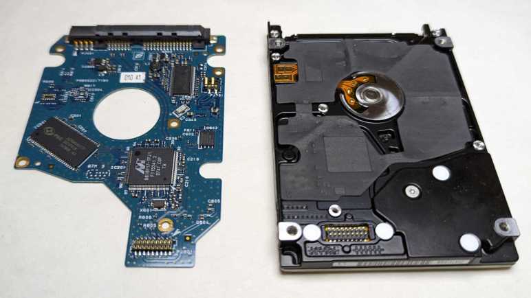
Putting a hard drive spindle motor’s control signals under an oscilloscope was instructive, even if I don’t yet understand everything that’s going on. Perhaps I could find some documentation to demystify the magic? I looked for hints on the hard drive control circuit board, which told us this 80GB drive dated from 2002 via “WDC (C) 2002” printed in the lower-left corner.
Motor control wires led to this chip, which has a ST Microelectronics logo. Unfortunately, putting these visible identifiers “L6278 17E H99SF0335” into ST.com site search came up empty. Either my search skills are pathetic, ST website database doesn’t go back that far, or this chip is something ST made exclusively for Western Digital under a proprietary contract. What’s certain is that I’m not going to learn more about this particular brushless motor controller. Oh well, I’ll continue my sightseeing tour.
Next chip over has a Marvell logo. And just like the ST chip, searching for “88C5540-LFE G472261.2 0339 B2S” came up empty.
Infineon TLE4417 is not listed on their own web site, but other sites (mostly trying to sell me some chips) say it is a voltage regulator.
If true, it makes sense to have voltage regulation close to the main controller: a WDC WD70C22.
A controller needs some working memory, which is where this Samsung K4S161622E-TC60 DRAM chip comes in.
I didn’t learn very much on this pass, but as I learn more about electronics, I hope future examinations will be more instructive and less of a just-for-fun sightseeing tour like this one. That is yet to be seen, in the meantime I retread familiar ground to take apart this hard drive’s mechanical components.
[UPDATE: Sprite took a stab at hard drive controller hacking some time back. Lack of datasheet documentation was a deal-breaking barrier for me, but not for the experienced hardware hacker.]
This device looks ancient but Fantom Drives appears to be still around today. Or possibly a company has acquired rights to that name and logo for doing business. The website lists a few internal M.2 SSDs but most of the product line are external USB storage drives. This is likely an early product of that line.
Size of this enclosure is consistent with a single 5.25″ floppy (or CD-ROM or DVD) drive bay. However, the front faceplate is empty with no slot for a disk.
Around the back we see a plug (IEC 60320 C13/C14) for power and a USB plug (type B) for data. A power switch and cooling fan rounds out the plate. I found the fan curious, because I don’t see any grille for intake or exhaust on this enclosure. Airflow would have been limited at best.
I see four screws on this plate. Two of them holds the fan in place, and the other two probably holds the USB data translation system in place. Neither look like a way for me to open up the box.
Four screws are visible on the bottom, and again they don’t look like something that’ll let me open the enclosure. They probably hold the storage device within.
I’m sure the warranty is long gone on this device, but I’m thankful for this “Warranty Void if This Seal is Broken” sticker because they would have placed it in a location critical to disassembly. Which is where I should start.
After the sticker was removed, the dark plastic clips on either side could be removed, allowing top and bottom enclosure halves to separate. Inside the enclosure we see… a standard 3.5″ hard disk drive looking pretty small inside that enclosure. It has a capacity of 80GB, giving an idea of how old this thing is. Nowadays we can buy cheap microSD cards with more capacity.
Another hint of its age is the antiquated parallel ATA interface used by this drive. I remember working on old PCs, fighting these huge and unwieldy cables. I do not miss them. Modern SATA (serial ATA) is so much easier to work with.
The spindle motor on this hard drive caught my attention: it is connected with four wires and not three like the hard drive motor I tried to turn into a generator. Could this be a pair of windings for two independent sets of coils? If so, I might try to run this thing using a stepper motor driver just to see what happens.
As for the electronics, I don’t know if I will ever find use for a board that translates between USB2 and PATA, two old and slow interfaces. The power supply is more likely to find reuse. I have a sizable stockpile of wall warts including several units with 12V DC output and several with 5V DC output. However, this particular power supply might come in handy if I ever need 12V and 5V together.
I thought the GMKtec NucBox3 looked interesting (at least on paper) as candidate ROS brain, so I ordered one (*) for a closer look despite some skepticism. All pictures on that Amazon listing look perfect, I suspected they were all 3D computer renders instead of photos of an actual product. There’s a chance the actual product looked very different from the listing.
The good news: the product is real and for the most part, as depicted in the listing. I find good fit and finish on its plastic enclosure. There is one downside: fingerprints show up very clearly. I had to wipe down the case pretty aggressively for these pictures and I still see greasy smudges. Well, at least you know these aren’t renders! One instance where oily fingerprint smudges are a feature, not a bug.
I see two brass heat-set inserts on the bottom of the case which will be useful for mounting this little box somewhere. They look very small but this is a small lightweight box so it would probably suffice.
Here we also see where actual product differed from product listing rendering. The company website page for NucBox3 showed an access panel to upgrade memory or storage.
But there’s no such access panel on the real thing, and it’s not clear how to get inside without one. Documents in the box consisted of a minimal warranty card in the box and no instruction manual. No matter, the lack of a convenient access panel or a manual shall not deter me from getting inside for a look.
Hiding fasteners under glued-on rubber feet is a common and effective technique. These four fasteners are not symmetrical so, even though the box is a square, we need to remember correct orientation to reinstall.
Without a convenient access door for upgrades, I wasn’t sure what else would differ from listing picture. I was afraid memory and storage would be soldered-in parts, but I was relieved to find they were standard DDR4 RAM and M.2 2280 SSD as advertised. They’re just a tiny bit harder to access without the panel.
Judging by its M.2 keys, we have the option to upgrade this factory-installed SATA M.2 SSD to a higher-performing NVMe M.2 SSD if needed.
What appears to be empty threaded holes (marked with circles) are actually used to secure the CPU heatsink from the other side. (There’s a fourth one under RAM module and not visible in this image.) Four fasteners (marked with squares) secure the motherboard and must be removed to proceed.
The headphone jack protrudes into the enclosure, so we must tilt the mainboard from the opposite side for removal. But we have to be careful because we are limited by length of WiFi antenna wires.
A block of foam keeps WiFi antenna connectors in place, peeling it back allowed the connectors to be released. The antennae themselves appear to be thin sheets glued to the top of the case, similar to what I’ve salvaged from laptops. How securely were they held? I don’t know. I didn’t try to peel them off.
Freed of WiFi wires, I could flip the mainboard over to see a big heatsink surrounded by connectors. As chock-full of connectors as this product already is, I was surprised to see that there are still several provisions for even more connectors on the circuit board. I’m also very fascinated by connectors used here for USB3, HDMI, and DisplayPort. I usually see them oriented flat against the circuit board as typical of laptop mainboards, but without design pressure to be thin, these connectors are standing upright. This is a tradeoff to fit more connectors on the edge of a circuit board, but each connector must go deeper to obtain the necessary mechanical strength to withstand use.
Looking in from the side, the heatsink appears to have a flat bottom. This is good news if I want to mount a different heatsink on this board, possibly with a fan. The flat bottom means I don’t have to worry about sticking out to make thermal contact with other chips or have to cut a hole to clear protrusions. If I want to mount to the same holes, I will have to drill four holes which unfortunately are irregularly spaced but not an insurmountable challenge. All that said, I’m more likely to just point a fan at this heatsink if heat proves to be a problem.
Using this computer as robot brain also means running it on battery power. Nominal power requirements are listed as 12V up to 3A. My voltmeter measured the factory power adapter output at 12.27V. But what can this thing tolerate? I found this chip directly behind the DC power barrel jack, but a search for DC3905 WK1MEG (or WX1MEG) didn’t turn up anything definitive. Texas Instruments has a LP3905 and Analog inherited Linear Technology’s LT3905. Both chips are designed for DC power handling, but neither footprint matches this chip. This might not even be the power management chip, I’m only guessing based on its proximity to the DC barrel jack.
As far as I know, the highest voltage requirement on this PC are USB ports at 5V. On the assumption that nothing on this machine actually needs 12V, then all power conversion are buck converters to lower voltage levels. If true, then this little box should be OK running directly on 3S LiPo power (Three lithium-polymer battery cells in series) which would range from 12.6V fully charged to 11.1V nominal to 10V low power cutoff. I’ll use the power brick that came in the box to verify everything works before testing my battery power hypothesis.
(*) Disclosure: As an Amazon Associate I earn from qualifying purchases.