Pinout of LCD Salvaged From AT&T CL84209

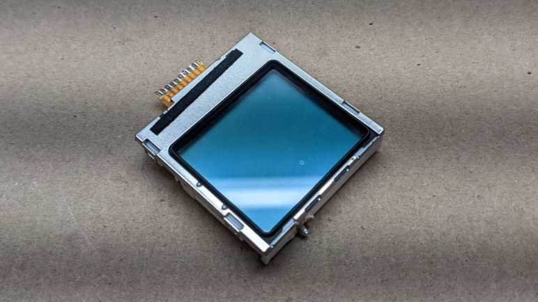
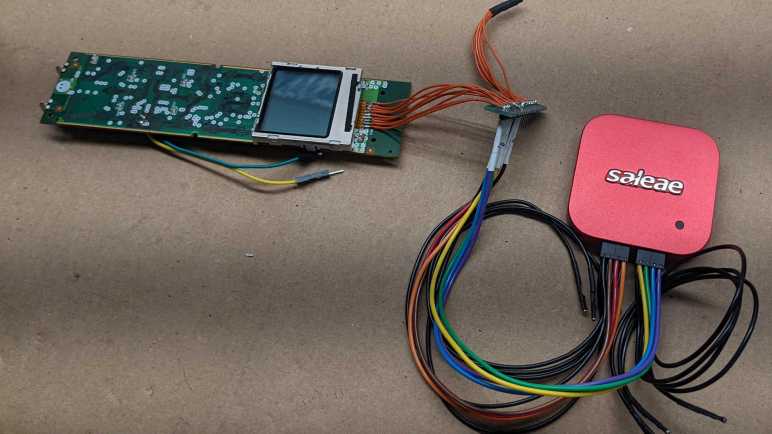
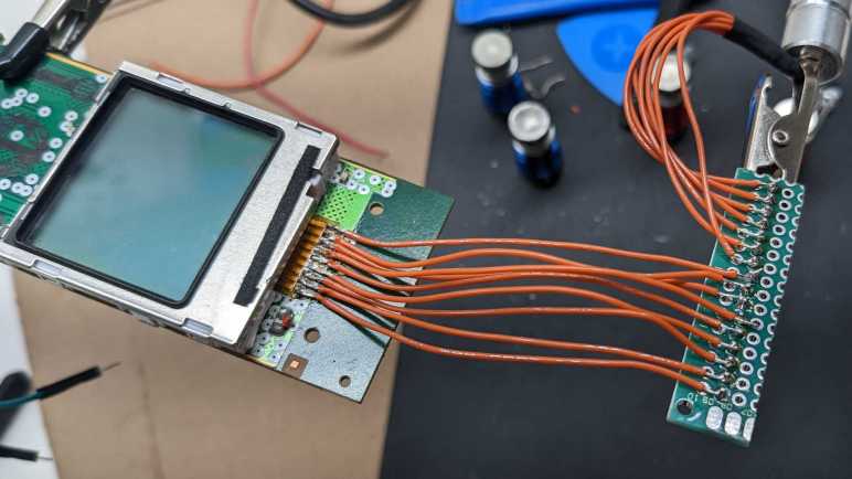
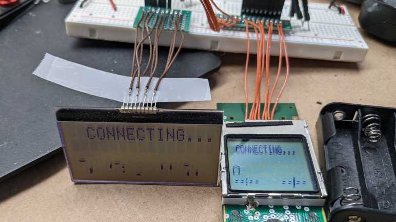
When I retired my landline phone connection, I also retired my home phone. It was an AT&T CL84209 phone with built-in digital answering machine. I had a base station and though it supported multiple cordless handsets I had just a single handset. Without a landline, I took the entire system apart keeping a few parts for potential later use. Among the stuff I kept were two custom LCD units. One LCD was freed from the base station circuit board. I wanted to keep its backlight as well, but I accidentally destroyed it while trying to free it from the system. The other LCD was in the handset, and I kept it attached to its circuit board because I didn’t want to accidentally destroy another backlight.

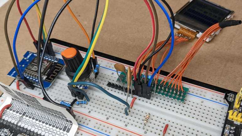
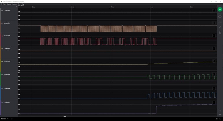
They sat in my pile of salvaged parts for several years, until a few weeks ago when I took them out and started playing with them. I thought I could find some official documentation on these display units, but nothing came out of searches using every identifier I could find on these devices. Fortunately, thanks to the still-working handset circuit board and a logic analyzer, I figured out enough to control them from an ESP8266 Arduino program. This page is a summary of my findings.

Electrical

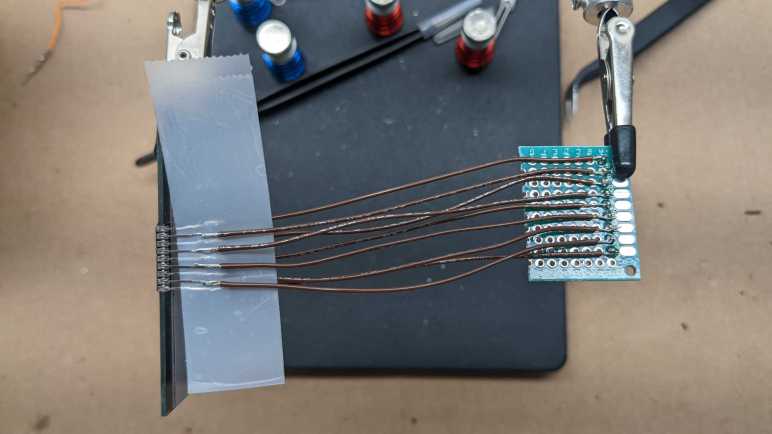
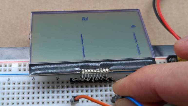
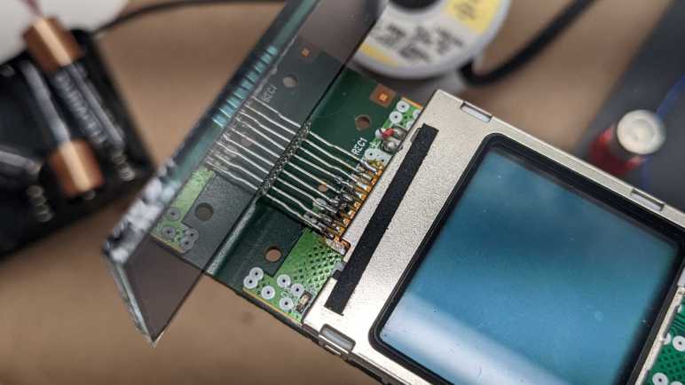
Both LCDs have nine hardware interface connections. Base station LCD uses pins, handset LCD shown above uses an FPC. I’ve numbered them 1 through 9 counting left to right as we are looking at the display. Despite the different physical form factor, electrically speaking they respond identically.

PinNameAdditional Notes
1EnableWe can make it always enabled by tying it high: use a 1kΩ pull-up resistor connected to pin 5 (+3.3V)
2SCLI2C clock logic level measured +3.3V, don’t know if it is +5V tolerant.
3SDAI2C data logic level measured +3.3V, don’t know if it is +5V tolerant.
4GroundRelative to pin 5
5VccSupply +3.3V to this pin.
0.82uF capacitor between this pin and pin 6 (Vboost)
6VboostOutput pin of built-in boost converter. Measured at +5.4V.
0.82uF capacitor between this pin and pin 5 (Vcc)
7VLCDHLCD segment voltage (high) 8kHz square wave from Vcc to Vboost
0.82uF capacitor between this pin and pin 8 (VLCDL)
8VLCDLLCD segment voltage (low) 8kHz square wave from 0V to Vcc
0.82uF capacitor between this pin and pin 7 (VLCDH)
9Voltage measured to match Vboost
Appears not connected to anything else on handset circuit board.

Digital

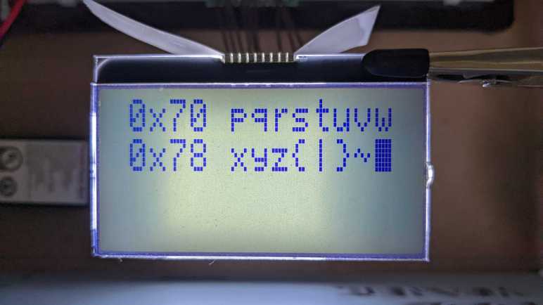
Both LCDs are I2C devices with an address of 0x3E. There are two types of messages:

  • Configuration set of 8 messages. Values were copied from logic analyzer capture and played back. Their exact meanings are unknown.
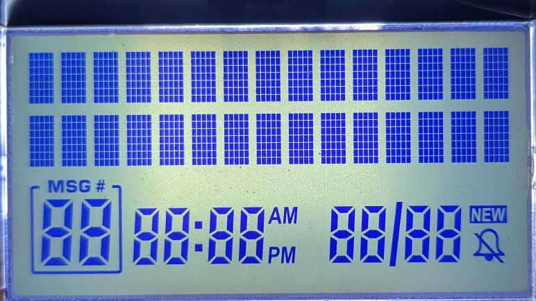
  • Data set of 3 messages. First message includes 15 bytes of alphanumeric data for the first line, second message for the second line, and the third message has 16 bits of digital data toggling state of custom LCD segments. (Which are different between LCDs.)

See the following pages for details:


Source code of software written to help with this investigation is publicly available on GitHub.

CL84209 Handset LCD Disassembly

I’ve mapped out the custom segments that occupy the lower half of this LCD, from the handset of an AT&T CL84209 cordless phone system. With that knowledge in hand, I wanted to dig a little more into this subassembly. When I removed it from the handset circuit board, I saw tantalizing hints of identification information that was mostly illegible through distorted plastic.

Four small sheet metal loops stamped in as part of the top metal shield held this assembly together. Once I popped those four loops freed of the tabs molded into the bottom-most piece of plastic, I could lay out all of its layers.

From left to right (bottom to top) we have:

  • Glossy injection-molded plastic bottom layer that is also most of the structural support.
  • Thin matte sheet of plastic.
  • Thicker (~1mm) clear sheet of plastic acting as conduit to distribute light from the single LED.
  • Thin frosted sheet of plastic acting as diffuser.
  • Glass LCD assembly with built-in I2C controller somewhere under the black blob.
  • Rubber surround (glued).
  • Topmost metal shield.

And now the objective of the exercise: a clear view of everything printed at the bottom of this handset LCD. Printed on a sticker is the following:

GWMS7728B
09470315313

Printed on the Flexible Printed Circuit (FPC) is:

7728-FPC-B-A152-4709

I see the logo of stylized “LCD” on both the FPC and etched into glass.

I saw the same logo on the base station LCD. And whereas that module was designated 6334, this one is clearly designated 7728 based on that number being repeated three times: etched into a layer of glass, on the white sticker, and also on the FPC connection.

This is a lot of additional information! Unfortunately, more information doesn’t guarantee success. Armed with this additional data, I still failed to find any details on this LCD module. But I’ll leave them here as a record hoping that my search skills will improve enough in the future to find something. But for today, I have to concede that I’ve tried everything I know. Lacking an official reference, I can only summarize all of my guesses about this device.

CL84209 Handset LCD Segment Map

Now that I’m properly driving this salvaged LCD, using its own voltage boost converter, I’ll map out its custom segments. The two lines of 15-character text uses the same character set as the LCD used in the base station of this AT&T CL84209 cordless phone system, but one space off from each other. On the lower half of the screen, this handset LCD has a different set of segments than the base station LCD. Fortunately, as they both respond to the same control protocol, I could use the same ESP8266 Arduino program to interactively select individual segments and write down which segment respond to which bits.

Comparing with the base station LCD segment map, there are some differences with obvious causes. For example, a battery gauge makes sense for the battery-powered handset. The battery outline segment (12) was an extremely informative element when I analyzed the digital control traffic, because it had been blinking on/off to signal low supply voltage and seeing that bit toggling on and off helped me zero in on the segment control bits. And now that I’m thinking about it, perhaps a blinking outline explains why 64 (outline around count of messages) and 100 (the actual “MSG#” text) are two separate segments. This was a design decision that puzzled me when looking at the base station LCD, but now I understand it gives the option of keeping “MSG#” on while the border blinks.

This handset LCD has a few additional custom segments, but two fewer 7-segment numeric digits. However, the hour tens digit of its clock area is thankfully a fully controllable 7-segment display, versus the base station LCD where all three horizontal lines were the same segment drastically limiting the digits it could display.

Numbering-wise, I see the “use 5 bits then skip 3” pattern. For example: 8, 9, 10, 11, 12 were used, then 13, 14, and 15 were skipped. I assume this has something to do with the segment/common convenience of wiring but couldn’t guess more without the chart like I had for Sanyo LC75853. Like the base station LCD, this handset LCD also skipped a byte entirely. Except in this case, it skipped the first byte (the first used bit was bit 8) instead of the final byte.

Putting together this segment map concludes the software side of exploring this LCD, I will now resume physical/mechanical exploration by taking apart this display assembly.


Source code for this investigation is publicly available on GitHub.

LCD Driver Has Own Voltage Boost Converter After All

I took apart an AT&T CL84209 cordless phone system and kept one of the handset’s circuit boards attached to its LCD unit. This allowed me to power up the circuit board and probe how its main processor controlled what’s shown on the LCD. I then took the LCD off of its board to take a closer look at the related circuitry.

Probing data indicated there was +5.2V on one of the LCD pins, and I had guessed it was supplied by a voltage boost converter somewhere else on the circuit board. I learned what they usually look like from the time I dug into the circuit board for a laptop screen, which included a boost converter to power its white LED backlight. On this handset circuit board, I see at least one assembly of an inductor next to a diode close to a capacitor, all the elements I now associated with a boost coverter.

But when I traced the phone handset circuit board, I didn’t find a +5.2V line going to the LCD. I found only a pair of capacitors. One of which connected the two square-wave generating pins (7 and 8) and another capacitor connected the +5.2V line to the +3.3V line. (Pins 5 and 6.) I don’t recognize what this arrangement does, but I could replicate it on my breadboard and see what happens.

The analog capture showed what happened: We now see pin 6 sit at 3.3V immediately upon initial power-up and rise up to +5.4V in response to the first I2C configuration message. Finally matching the pattern I saw on the original capture. This is amazing! The LCD driver chip only needs a +3.3V power supply and from that it generates its own +5.4V. There must be a built-in voltage boost converter with inductor and diode (or their functional equivalents) internal to work alongside an external capacitor. I thought I had learned enough about boost converters to recognize them when I see them, now I know I’m wrong. Earlier I had put a capacitor between the boost converter output line and ground, and that didn’t do what it did when I put the capacitor between boost output and +3.3V. I clearly have more to learn more about boost converters. But at least now I’m finally driving this LCD properly.

Unsoldering CL84209 Handset LCD

After mapping out the segments on the LCD salvaged from the base station of an AT&T CL84209 cordless phone system, I have reached the limits of what I can do in the absence of additional information. It has been wonderfully instructive to have a handset from the same system with its own LCD. I found that both LCD respond to the same command protocol, so I could power up the handset circuit and watch what happens under a logic analyzer then try to replicate the same behavior for the base station LCD. Now it is time for me to remove the LCD from the handset circuit board. I wanted to do so for two reasons:

  1. I don’t really want to keep the entire handset circuit board. It is designed to talk to a base station that no longer exists.
  2. It might be hiding some useful secrets underneath the LCD. I have a working knowledge of how all the pins work, but I might learn more from probing the circuit board independent of the LCD.

A bit of time with the solder station and I have separated the LCD to see that there’s… almost no components hidden underneath.

Just a single side-illumination LED in the upper right corner marked LED3. It feeds into a backlight mechanism much less sophisticated than a Fire tablet’s backlight.

But now we can see copper traces on this side of the circuit board. I was happy to see that my arbitrary left-to-right pin numbering matched what’s silkscreened here, purely by accident! I had thought pin 1 or 5 could be the power supply, and decided 1 was enable and 5 was supply. Now I get confirmation because 1 is a very narrow signal trace and 5 is a much thicker power trace. 2 and 3 were also thin digital signal lines for I2C, and 4 is connected to a big grid-patterned plane consistent with ground.

Those were great confirmations of my earlier guesses, but even better is information about the rest of the pins. The surprise was that pin 9 appears to be connected, because I had thought it was one of the capacitors I saw on the back side. Another surprise is that pin 6, which I thought would connect to a +5.2V supply, seems to connect only to one of four vias (marked by white circles) going to the other side of the circuit board.

Following those four vias to the other side, I find a pair of capacitors. Now that the LCD has been unsoldered, my multimeter could measure their capacitance: the one on the left read 823nF and the one on the right 775nF. Looking over popular capacitors on Digi-Key, these might be 0.82uF +/- 10% capacitors. But even more importantly: now that I can see the traces, I understand one capacitor bridges the +3.3V line and the +5.2V line, and the other bridges the two square wave lines. My electronics knowledge isn’t good enough to know what this means. But once I replicated this part of the circuit, I saw a voltage boost converter in action.

CL84209 Base Station LCD Segment Map

I have generated a printable lookup chart for the character set of an unknown LCD controller. This chip is embedded inside a black blob along the top edge of an LCD I salvaged from the base station of an AT&T CL84209 cordless phone system. The character set dictates what is rendered in two lines of 15-character alphanumeric text, each character is a dot matrix 5 pixels wide and 7 pixels tall. Below these two lines is a set of custom segmented LCD that can be controlled with 16 bytes, but there appear to be far fewer than 16*8 = 128 segments to control. A segment map will tell us which segments correspond to which bits.

I don’t have the datasheet for this chip, so I don’t know how it numbered its segments. I decided to mostly follow the precedence set by Sanyo LC75853 by numbering both bits and bytes in least-significant-first order. The difference for this map is that while LC75853 started counting from one, I’m going to start counting from zero.

My first attempt at mapping out these segments toggled them on/off alongside the character set data. When displaying characters starting with 0x00, I turned on all the segments whose number has zeroth bit set. For the character set starting with 0x10, I turned on all the segments with the next bit set, etc. In theory I could look at the on/off pattern as it cycled through 0x00 to 0x70 and determine its binary number. I also printed out the bit pattern to Arduino serial console, which looks like this:

0 1 10101010 10101010 10101010 10101010 10101010 10101010 10101010 10101010 10101010 10101010 10101010 10101010 10101010 10101010 10101010 10101010 
1 10 11001100 11001100 11001100 11001100 11001100 11001100 11001100 11001100 11001100 11001100 11001100 11001100 11001100 11001100 11001100 11001100 
2 100 11110000 11110000 11110000 11110000 11110000 11110000 11110000 11110000 11110000 11110000 11110000 11110000 11110000 11110000 11110000 11110000 
3 1000 0 11111111 0 11111111 0 11111111 0 11111111 0 11111111 0 11111111 0 11111111 0 11111111 
4 10000 0 0 11111111 11111111 0 0 11111111 11111111 0 0 11111111 11111111 0 0 11111111 11111111 
5 100000 0 0 0 0 11111111 11111111 11111111 11111111 0 0 0 0 11111111 11111111 11111111 11111111 
6 1000000 0 0 0 0 0 0 0 0 11111111 11111111 11111111 11111111 11111111 11111111 11111111 11111111 
7 10000000 0 0 0 0 0 0 0 0 0 0 0 0 0 0 0 0 

In theory this can work, in practice I quickly got tired flipping through images and decoding binary numbers by hand. That was a lot more work than having a quadrature encoder knob to interactively select segments to activate. I had avoided wiring in extra components out of laziness, but between manual binary decoding and soldering, I decided a bit of soldering was the easier path towards this segment map:

This map clearly showed this particular segment allocation used less than 5/8 of available segments. Starting from position zero, we would have five bits for five segments (0, 1, 2, 3, 4) then three bits that were unused. (5, 6, 7) Then five more segments (8, 9, 10, 11, 12) and three unused bits (13, 14, 15). This repeats until the final set of five (120, 121, 122, 123, 124) which were also unused.

I was surprised that segment 9 (“MSG#” title for message count) was a separate segment from 4, the rectangular border around message count. I had expected them to be a single segment.

I was also surprised and annoyed at segment 27, which lights up all three horizontal lines of the hour tens digit for the clock plus the lower left vertical segment. For a clock it made sense to restrict the tens digit to 1 or 2. But if so, why did they bother with segment 26 which isn’t useful for either of those digits? I had hoped maybe I could use it as a generic numeral display and not a clock, by leaving 65 and 66 (AM/PM) inactive. But segment 27 means I could only display 1, 2, 6, and 8. I have not yet thought of an interesting non-clock usage under those restrictions.

Obtaining a full segment map marks the end of investigating this base station LCD, I will now try to do the same for the handset LCD starting with its disassembly.


Source code for this investigation is publicly available on GitHub.

CL84209 Base Station LCD Character Set

After a look at the similarities and differences between two LCDs salvaged from an AT&T CL84209 cordless phone set, I was ready to start controlling one myself to get more data. Earlier probing indicated that I2C communication on the handset was 3.3V, so I’m going to use an ESP8266 because it is also a 3.3V part. The Arduino platform should be a good (enough) starting point, using its Wire library to recreate the I2C control messages I saw sent to the handset LCD.

After a quick test program to verify things worked as expected, I wanted to dump out the character set built inside this LCD controller. Since the character data is sent one byte per character, there are potentially 256 different characters in the font. Dealing with these powers-of-two numbers, I like to keep such information lined up with their hexadecimal values. The LCD can only print up to 15 characters per line, so I couldn’t print these in 16 characters batches. As a next best thing, I dropped down to 8 characters per line along with their starting hexadecimal value. A for() loop cycled through 16 such screens once per second, so I could see the entire character set cycle through.

This is one of the sixteen steps in the cycle. The first line shows characters from 0x70 to 0x77, and the second line from 0x78 to 0x7F. Using workbench lighting, I had trouble trying to photograph the screen without glare. So, I switched to backlighting the LCD using one of my salvaged LED backlights. I took a picture for each of the 16 sections with the intent to edit them together, but the slightly undersized backlight made it difficult. The center section of the screen is noticeably brighter than the edges, which makes it difficult to set a threshold to generate a nice monochrome reference chart. I had to consult Emily Velasco for some photo-editing tips. (I have now added “burn” & “dodge” to my photo editing toolbox.) After some very informative experimentation in GNU Image Manipulation Program I have a reference sheet suitable for printing. Using this chart, I could see that 0x7F is a solid block that activates all pixels of a 5×7 dot matrix, which I will use to as part of an “turn everything on” program to help map out its adjacent segmented region.


Source code for this investigation is publicly available on GitHub.

Handset LCD versus Base Station LCD (CL84209)

I have two LCD units salvaged from an AT&T CL84209 cordless phone system. One from the base station, and one still attached to a handset circuit board. The handset could still be powered up and ran, which helped me figure out how to interact with the base station LCD’s digital logic and analog voltage supply pins. Connecting them in parallel was a bad idea in many ways, but the risky experiment paid off telling me they both responded to the same I2C address and displayed similar but not identical things. Now that I have them side by side again, with some confidence I’m not damaging them while doing so, I have time to take a closer look at the similarities and differences.

Both of these LCDs have two lines of dot-matrix display on top, and a custom segmented LCD area below that. Each of the two lines consist of 15 characters, each character a dot matrix 5 pixels wide and 7 pixels tall. Its I2C control data indicates pixel-level control is not possible, since we only send a byte of data for each character. This is apparently tailored for alphanumeric information and not a full graphics display.

Curiously, given that both LCDs have two lines of 15 characters each, they seem to be one space off from each other when given identical control messages as they are here. For the base station LCD, we see two spaces in front of “CONNECTING…” and no space behind. In contrast, the handset LCD has that text centered on screen with one space in front and behind. If one of these screens had 15 characters and the other had 16, I could understand rendering one space off. But they both have 15 characters, so why would they do this?

The segmented area appears to be completely different between these two LCDs. Looking at the I2C traffic, 16 bytes were sent for 16*8 bits = up to 128 potential segments for control. Some of those bits go unused, as neither of these LCDs have 128 segments. For the handset LCD, I count 10 segments used for “–:– –/–” and an 11th for the battery icon. The same control bits just result in a nonsensical jumble of segments on the base station LCD, but I count 11 active segments in that jumble. It’s obvious they don’t have the same segments, but perhaps they use a similar subset that would be easiest to wire up in a LCD. I expect to get a better understanding once I start controlling this LCD with my own code.

LCD Behavior Between 5V Power Supply Candidates

There were nine pins on an LCD salvaged from an AT&T CL84209 cordless phone system. I found two candidates for its +5V power supply pin, but an experiment found that they both seemed to work. I doubt these are both +5V supply pins, as I expect the manufacturer would have removed unnecessary redundancy in the interest of cost. I hypothesize that one of them is the actual +5V supply pin, and the other one allowed +5V to leak through the circuit as an accidental side effect. Trying to guess which is which, I returned to recording analog behavior with my Saleae Logic 8.

For reference, here’s the behavior of handset LCD start-up that I want to replicate for pins 6-9. (Channels 4-7.)

The first experiment was to turn on the system without connecting any of the four mystery pins.

Channel 5 picked up 3.3V from elsewhere in the circuit. Channel 4 less so at 3V. The other two pins would sporadically spike up to one of those two voltages. This is definitely wrong, but I wanted to rule out the possibility this mystery LCD controller had a built-in voltage booster.

The next experiment was to put +5V (well, 4.8V) on Channel 4.

This looks much better. Channel 5 and 6 behavior looks correct, or at least close enough to my eyes. I don’t see anything that makes me think “Hmm, maybe this pin needs an external inductor, resistor, or capacitor.” Such as channel 7, who is trying and failing to hold 5V so I think it needs an external capacitor.

Then I switched +5V over to channel 7:

Channels 5 and 6 are again working roughly as expected, which explains why LCD segments look good no matter where +5V comes in. However, I see a weird multi-step behavior on channel 4 that is not ideal. Out of my options, I think I should put +5V on channel 4 and put a little capacitor (100nF ceramic) on channel 7:

Yeah, I think that’s my best approximation to the ideal behavior. The only difference I see is that, on the original data, channel 4 started with 3.3V then jumped up to 5V upon startup. It seems to be under LCD startup control, but I don’t see how. Maybe there’s something contributing elsewhere on the circuit board? I know there are still mysteries on this circuit buried underneath the handset LCD, something I intend to investigate later. For now, I hope putting +5V on pin 6 (channel 4) before initialization would not damage the LCD, because I plan on doing that for further exploration. Starting with a comparison between these two LCDs both responding to I2C 0x3E.

LCD in Parallel Test Round 2: 5V Power

There were nine pins on this LCD unit salvaged from an AT&T CL84209 cordless phone system. I think I’ve figured out five of them: 3.3V supply, ground, enable, I2C clock, and I2C data. The remaining four are still unknown but I noticed a correlation between their start-up behavior and the first control message sent to its I2C address of 0x3E. Perhaps those pins are not all input pins?

To get more data, I’m going to repeat the experiment of connecting two LCDs in parallel. One still mounted on remnant of a CL84209 handset circuit board, and the other was a bare module from the base station. The first time I tried this harebrained scheme, I connected all nine pins. Both displays ran, but at much lower contrast than usual.

This time, I won’t connect all the pins. Power supply, ground, and enable pins should be safe to connect in parallel. I2C data and clock lines are designed to connect to multiple devices in parallel, so electrically speaking it should be fine as well. But I2C is not designed to have two devices responding to the same address connected together. The protocol has no provision for such conflict resolution and usually I2C address conflict leads to chaos. The only reason we can get away with it this time is because these two screens respond identically (or close enough) so there aren’t conflicts to resolve.

With five out of nine pins connected in parallel, I will experiment to see what happens when I selectively connect the rest. For reference, here is the behavior recorded from the handset running standalone: Channels 4 and 7 should rise to 5V, channel 5 should be an 8kHz square wave between 3.3V and 5V, and channel 6 should be another 8kHz square wave from 0V to 3.3V in phase with channel 5.

Looking at this plot, I think I need to connect at least a pin to serve as a 5V power supply. Pin 6 (channel 4) and pin 9 (channel 7) are both candidates for 5V supply, since they both rise to 5V once things started up. Before the startup procedure, pin 6 (channel 4) received 3.3V as soon as the system received power, while pin 9 (channel 7) stayed at 0V until the startup procedure. Based on this difference, I think pin 6 (channel 4) is the better candidate to try, so I added a jumper wire to connect that to the handset circuit board.

It’s alive! And better yet, display contrast on both screens appears normal. Not faded-out as I saw in the previous parallel test with all nine pins connected.

Normal display contrast supports the hypothesis that the 8kHz voltage square waves were used for LCD segments, and furthermore this test implies those square waves were generated by the onboard controller. When these two LCDs were connected in parallel, their 8kHz voltage waves interfered with each other and lowered contrast on both. But if this is true, why do these signals need to be brought out as externally accessible pins? Why not just leave them internal? I don’t have a good guess for that.

As an additional data point, I disconnected pin 6 and connected pin 9. If my hypothesis is correct that pin 6 is the 5V power supply, disconnecting it and putting 5V on pin 9 should mean the display stays blank. Nope! My hypothesis was wrong or at least incomplete. When I disconnected pin 6, the display went blank as expected. But when I connected pin 9, the display came back to life. Both pin 6 and pin 9 could apparently serve as 5V power supply. Which one should I use? Perhaps taking another set of analog traces could provide some insight.

LCD Analog Activity Started By Digital Signal

I feel I have a working understanding of the I2C control messages necessary for controlling an LCD salvaged from an AT&T CL84209 landline phone system. But that is only part of the puzzle, because this LCD had input/output pins beyond I2C clock and data lines: there were four more pins to figure out. Represented by channel 4-7 in this logic analyzer trace:

Upon system power-up, one started at 3.3V and the others at 0V. Roughly two seconds after power-up, they come alive with two of them going up to 5.2V and the other two generating ~8kHz square waves. One between 0V and 3.3V, the other between 3.3V and 5.2V. I had assumed I would have to build circuitry to mimic these voltage values, but maybe I wouldn’t.

When zoomed in to when these pins became active, I could see the analog activity was immediately preceded by activity on the I2C bus. Comparing the timestamp against the list of decoded I2C messages, I found the I2C message visible on this graph is actually the very first set of messages sent to the LCD at address 0x3E.

This implies the LCD is not just a passive receiver of these signals, but an active participant who started something in response to the first initialization command sent over I2C bus. What we see here is some combination of functionality onboard the embedded chip, and some contribution from the circuit board. But I have no guesses at the division of labor between them. I assume the circuit board must contribute something to the process, otherwise the embedded controller could have just kept things internal and not incur the manufacturing cost of bringing those pins out.

I looked to the Sanyo LC75853N LCD controller datasheet I previously referenced for a different device to see if it had a counterpart to these pins. I note the OSC pin that required an external resistor and capacitor, and the VDD1 and VDD2 pins that required external voltage supply. None of these explanations fit the two pins that rose to 5.2V. The square wave between 0V and 3.3V might be an external oscillator, but I don’t know what that means for the other square wave between 3.3V and 5.2V.

On a quest for more data, I am going to try wiring these two LCDs in parallel again. The previous time was a risky experiment done in ignorance armed only with the fact I had very little to lose. This time I’m a little better informed which I hoped should translate to lower risk on the second try.

Examining Control Data for LCD at I2C Address 0x3E

My Saleae Logic 8 listening to the communication traffic on the I2C data bus of an AT&T CL84209 cordless phone headset heard thousands of messages within ten seconds of startup, addressed to ten different device addresses. I only cared about the messages related to its LCD screen and, fortunately, that data stood out and now I know this LCD is an I2C device with address of 0x3E.

Curious if knowing the I2C address will help me find more information on this LCD, I went online and… didn’t have much luck. Adafruit organizes a list of their I2C product addresses, but as of writing there’s nothing listed for 0x3E. I found the JHD1313 LCD module online, whose AiP31068 controller is an I2C device on address 0x3E. This chip is controlled with a series of command words, which is a control byte followed by a data byte. Different from the pattern I see on my Saleae decoded data, where character data is sent consecutively without command bytes in between. (Also, the datasheet annoyingly doesn’t give its I2C device address in hexadecimal or decimal form, only in binary form “011 1110” in the serial interface protocol chart.)

Empty-handed from this detour, I returned to my Python program parsing Saleae-decoded output. Out of 2569 captured messages, only 143 of them (5.57%) were addressed to 0x3E. This is a much more manageable number. Looking at that set, I found there were many two-byte messages and a few of the longer 18/19 byte messages.

The sequence of two-byte messages is almost identical throughout the capture, only difference is that the very first instance is one message shorter. (It omitted the final 0x00,0x02.) After that, the whole sequence repeats once every second. Lacking datasheet, I’m calling this the configuration sequence.

write to 0x3E ack data: 0x00 0x39 
write to 0x3E ack data: 0x00 0x1C 
write to 0x3E ack data: 0x00 0x70 
write to 0x3E ack data: 0x00 0x5F 
write to 0x3E ack data: 0x00 0x6C 
write to 0x3E ack data: 0x00 0x0C 
write to 0x3E ack data: 0x00 0x02 (Omitted from initial startup)

Shortly after this is sent, three lines of display data are sent. The capture included three variations. The first one is sent only once, immediately after the initial configuration sequence is sent:

write to 0x3E ack data: 0x80 0x81 0x40 0x20 0x20 0x20 0x20 0x20 0x20 0x20 0x20 0x20 0x20 0x20 0x20 0x20 0x20 0x20 
write to 0x3E ack data: 0x80 0xC1 0x40 0x20 0x20 0x20 0x20 0x20 0x20 0x20 0x20 0x20 0x20 0x20 0x20 0x20 0x20 0x20 
write to 0x3E ack data: 0x80 0x40 0x40 0x00 0x00 0x00 0x00 0x00 0x00 0x00 0x00 0x00 0x00 0x00 0x00 0x00 0x00 0x00 0x00 

The first two lines are all spaces, and the third line is all zeros. I interpret this as the “clear screen” for this LCD.

Afterwards, we have two variations of display data with “CONNECTING…” text. The first one:

write to 0x3E ack data: 0x80 0x81 0x40 0x20 0x43 0x4F 0x4E 0x4E 0x45 0x43 0x54 0x49 0x4E 0x47 0x2E 0x2E 0x2E 0x20 
write to 0x3E ack data: 0x80 0xC1 0x40 0x20 0x20 0x20 0x20 0x20 0x20 0x20 0x20 0x20 0x20 0x20 0x20 0x20 0x20 0x20 
write to 0x3E ack data: 0x80 0x40 0x40 0x00 0x00 0x10 0x02 0x01 0x04 0x00 0x10 0x00 0x04 0x01 0x00 0x02 0x10 0x04 0x00 

Differs from the second one by only a single bit in the third line, 0x00 vs. 0x10:

write to 0x3E ack data: 0x80 0x81 0x40 0x20 0x43 0x4F 0x4E 0x4E 0x45 0x43 0x54 0x49 0x4E 0x47 0x2E 0x2E 0x2E 0x20 
write to 0x3E ack data: 0x80 0xC1 0x40 0x20 0x20 0x20 0x20 0x20 0x20 0x20 0x20 0x20 0x20 0x20 0x20 0x20 0x20 0x20 
write to 0x3E ack data: 0x80 0x40 0x40 0x00 0x10 0x10 0x02 0x01 0x04 0x00 0x10 0x00 0x04 0x01 0x00 0x02 0x10 0x04 0x00 

This is consistent with handset LCD behavior blinking the “battery low” icon in the custom segmented LCD area. From here we can tell the first two lines are alphanumeric text, and the third line are bits for segmented LCD control where 0 is clear and 1 is active.

Looking at the screen, I see the battery icon blinking once a second. (Half second on, half second off.) Given this, I had expected to see the two variations of display data to alternate. Instead, it’s usually two of one style followed by one of the other. This mystery was solved once I looked at the timestamps: once every second, the configuration sequence is sent immediately followed by the current display state. Even if the display state hadn’t changed from the previous display update. In between these configuration sequences, the battery icon state is toggled every half second without sending the configuration sequence.

Thanks to Saleae Logic software and a bit of Python, I feel I’ve gained a working grasp of digital control communication for this LCD. I don’t know what any of those control flags individually mean, but I wouldn’t need to fully understand them if I just wanted to send alphanumeric data and toggle segments. Outside of these digital signal pins, there’s still the unknown of analog voltage pins. But looking at the timeline, I noticed an interesting correlation.

Cordless Handset LCD is I2C Device

I’m working to understand how to control the LCD on the handset of an AT&T CL84209 landline phone system, and I started by observing the behavior of its eight IO pins (plus one pin already established to be ground) using the analog mode of my Saleae Logic 8 analyzer. Two pins were immediate candidates for a serial data pin and its corresponding clock pin, so I switched my analyzer to digital mode observing those two pins specifically.

Mouse hovering over the clock line, the analyzer software told me it started at a frequency of 7.2kHz and then sped up to 100kHz during the startup sequence. 100kHz is very promising, because it matches “Standard Mode” speed of I2C. The previous LCD controller I played with used a proprietary Sanyo protocol called CCB, but I’m hopeful this unknown chip uses Philips I2C. So in the spirit of “be sure to check the easy thing first” I activated I2C protocol analyzer built in to Saleae’s software. This presented a stream of decoded bytes and no sign of error.

Good news: it is indeed I2C!

Bad news: within less than ten seconds of powerup, there are 2569 captured and decoded messages. That is a lot of raw data to wade through when I don’t datasheets to make sense of it all. But the situation isn’t quite as bad as it initially looked. While I’ve tapped pins directly connected to the LCD, that doesn’t mean all the data we see on those lines are relevant. I2C is a data bus for multiple devices to communicate, and I see multiple addresses listed in the I2C decoder output.

I wanted to filter messages by address, but I failed to find such an option in Saleae software. Instead, I copied the data output into a Jupyter notebook and wrote a bit of quick-and-dirty Python to parse them. There were ten unique I2C addresses in this output:

{'0x52', '0x51', '0x50', '0x56', '0x3E', '0x53', '0x54', '0x55', '0x4B', '0x57'}

Scrolling through the decoder output, traffic to address 0x3E stood out because they were the longest. Many of these I2C messages had only one or two bytes, but some messages to 0x3E were much longer. The long messages have a pattern, they come in sets of three: two 18-byte messages followed by one with 19 bytes.

write to 0x3E ack data: 0x80 0x81 0x40 0x20 0x43 0x4F 0x4E 0x4E 0x45 0x43 0x54 0x49 0x4E 0x47 0x2E 0x2E 0x2E 0x20 
write to 0x3E ack data: 0x80 0xC1 0x40 0x20 0x20 0x20 0x20 0x20 0x20 0x20 0x20 0x20 0x20 0x20 0x20 0x20 0x20 0x20 
write to 0x3E ack data: 0x80 0x40 0x40 0x00 0x00 0x10 0x02 0x01 0x04 0x00 0x10 0x00 0x04 0x01 0x00 0x02 0x10 0x04 0x00 

These messages won’t have enough bits to control individual dots on the dot-matrix display. However, they might contain alphanumeric data for the LCD controller to use a font lookup table. Again, in the spirit of trying the easy thing first, I compared the first line of data against an ASCII chart.

0x800x810x400x200x430x4F0x4E0x4E0x450x430x540x49ox4E0x470x2E0x2Eox2E0x20
[?][?]@[space]CONNECTING...[space]

“CONNECTING…” is the first line displayed on the LCD! We have a winner, time to dig into traffic addressed 0x3E for this I2C LCD.

Cordless Handset LCD Power-Up in Saleae Analog Mode

I have the remnants of a cordless handset from a AT&T CL84209 landline phone system. It can still power up enough to put “CONNECTING…” on its LCD and I want to learn how to talk to that LCD myself. To do this I’ve attached wires to that LCD so I could probe its control signals with my Saleae Logic 8 analyzer.

Before I get to the digital signal analysis, though, I need to be sure I’m listening on the correct lines. This is why I connected all eight potential data lines (plus the one known ground I probed earlier) to watch them all at once with my Saleae running in analog mode. This is a secondary capability for the device and while it cannot replace a real oscilloscope it is nevertheless very useful to me as I only have a cheapo single channel oscilloscope with unreliable voltage levels. While I might buy a real multi-channel oscilloscope in the future, it is unlikely to be an eight-channel unit.

Here is the handset power-up sequence, and roughly eight seconds after power is supplied:

When I probed with a voltmeter, pin 1 (channel 0) and 5 (channel 3) were candidates for 3.3V input power. With this graph, I see square wave dips in channel 0 that indicate an enable signal, so pin 5 is +3.3V. Which makes some sense as it is adjacent to ground on pin 4.

After pin 1 enable signal stayed high, right around the 2 second mark, something significantly happens where we saw activity on channels 4-7. Here is a zoomed in view of that time period:

Pin 3 (channel 2) looks like data bits clocked by pin 2 (channel 1). I’ll look at them more closely later in digital analysis mode.

We also see the beginnings of startup on remaining four pins of unknown:

  • Pin 6 (channel 4) had 3.3V as soon as power is applied to the system, and later it jumps up to 5.2V and stays there.
  • Pin 7 (channel 5) likewise had ~3.3V immediately upon power up, and when pin 6 jumps up to 5.2V it oscillates between 3.3V and 5.2V.
  • Pin 8 (channel 6) started out flat at 0V, but would oscillate between 0V and 3.3V.
  • Pin 9 (channel 7) started out flat at 0V, but would jump up to 5.2V and stay there.

The two oscillating pins are both square waves and they move in phase. (Rise and fall at the same time.) The period from one rising edge to the next is about 125us, translating to 8kHz.

Zooming out on the timescale, I see no signs of data modulation on these pins:

I think these are voltages applied to LCD segments. It would be easy for me to replicate pin 8 square wave of 0V to 3.3V with a 3.3V microcontroller like ESP8266, but it’s not clear how I would replicate pin 7 square wave between 3.3V and 5.2V. A headache I will set aside for later.

The relationship between pins 6 and 9 is puzzling. Since pin 6 had 3.3V immediately upon powerup, and its voltage started rising before the other three pins, I thought it was the best candidate for a 5.2V power supply rail. My hypothesis was that it is connected to a boost converter external to the LCD that would pump the 3.3V up to 5.2V. The counterargument is the fact that pin 9 reached 5.2V before pin 6 did, so I’m not sure what’s going on.

While I think over the analog voltage startup behavior puzzle, I switched my logic analyzer to digital mode (what it’s designed for) for a look at the digital data and clock lines.

Preparing Cordless Handset LCD for Logic Analysis

I’ve decided to take another look at a pair of LCD units salvaged from an AT&T CL84209 landline phone system. I have a bare LCD from the base station, and an LCD still attached to the remnants of a cordless handset. I had wired those two LCDs in parallel, a crazy roll of the dice that paid off in knowledge that those two LCDs use the same communication protocol. Now I am armed with a logic analyzer (Saleae Logic 8) and intend to get more details.

The first step is to attach wires to the handset LCD so I could probe communication traffic, similar to how I attached the bare LCD earlier but with less risk and higher chance of doing something useful. I recycled the bundle of wires I had used to perform the same task on a Toyota tape deck faceplate, which had more wires that I folded out of the way for this project. Having done similar tasks a few times, I’m starting to think about buying PCBite probes that promise to let me skip this soldering task. But I’m not yet at the point where I expect to use them enough to justify the expense.

There are nine pins on this LCD, which given my lack of official datasheet I’ve arbitrarily numbered from left to right as shown in the picture above. Earlier I had probed these connection points with a voltmeter while the handset circuit board was running. All of the pins appear to be safely within Saleae logic analyzer 25V limit relative to ground, which I determined to be pin 4. That left 8 pins I don’t understand and conveniently, my Saleae has 8 inputs so I could connect them all and not have to make decisions on which pins to omit. Once connected, I could take my first look with the Saleae in analog mode.

LCD Exploration Unwinds Back to CL84209

In my electronics teardown and salvaging adventures, I kept a few segmented LCD units with the intent to learn about them later. After I watched Joey Castillo’s Remoticon presentation on LCDs, I decided it was time to take some LCDs out of my pile and start learning how to use them.

In hindsight, I undertook this adventure in backwards order. I couldn’t make heads or tails of my first attempt, and the second didn’t fare much better though it gave me enough information to infer those two LCDs both came from an AT&T CL84209 wireless landline system. The third attempt was a car tape deck I managed to power up, but it was too advanced of a system and wouldn’t help me learn LCDs basics. The fourth item was an LCD salvaged from a food thermometer, but I had problems trying to attach wires to this display. I was finally successful on the fifth try, obtaining full control over a simple segmented LCD salvaged from an electric blanket controller.

After that success, I started unwinding my stack of failures. A bit of hackery and a lot of patience allowed me to map out the food thermometer LCD on my second try.

With these two examples of low-level LCD control, I returned to the tape deck and learned how to work at a higher level with its LCD controller. I even learned a new communication protocol (Sanyo’s CCB) and programmed an Arduino Nano to speak its language.

Obtaining a full understanding of how to interface with the faceplate was very satisfying. Two key factors made it possible: the LCD controller’s datasheet, and a Saleae logic analyzer.

Armed with this experience, I will now return to where I started: to the mystery LCD units salvaged from an AT&T CL84209 landline phone system. I found nothing to identify their LCD controller, so I would have to go without a datasheet. However, I do have one valuable datapoint: a risky experiment proved that while those two LCDs were different, they do communicate with the same protocol. This is enough of a starting point for me to dive in with my logic analyzer.

Risky Parallel LCD Test Surprisingly Worked

I briefly surveyed LCD controllers popular with hobbyist projects, hoping to find something that might match my mystery salvaged LCD units on hand. No luck. If my intention is to build a project with LCD screen, I should go and buy one of those popular units. But the point of the exercise is to try reusing salvaged electronics, so I stared at my two LCD units some more while thinking of Emily’s observation that they both had nine interface pins and the hypothesis they share a common command set.

I know for sure they aren’t identical. For starters, the two modules are different sizes. And while they both have nine interface connection; they are physically different. The bare LCD module has pins, and the headset LCD module is soldered to its circuit board with a segment of FPC (flexible printed circuit). Holding the bare LCD’s pins up to those soldered joints, I had an idea: what if I wired both LCDs together in parallel by soldering the bare LCD pins to the existing FPC pads?

The first thought was to dismiss it as a stupid idea. There were too many reasons why it wouldn’t work even if the devices have a common interface. If they were SPI devices, they would conflict on the MISO pin. If they were I2C devices, the two devices probably have different addresses, and the bare LCD wouldn’t do anything. Or if they had the same address, there would be conflict as they both tried to ground I2C control lines at the same time. LCD controllers like the PCD8544 had internal LCD voltage generators. Wiring two boost converters in parallel risks creating a feedback cycle that overshoots limits and destroy components. And if their wiring were completely different, I risk short-circuiting VCC to ground, or possibly connecting one of the boosted higher voltage lines to something that could not tolerate such voltage. And I’m sure there are other risks that didn’t come immediately to mind.

But despite all those risks, the thought refused to go away. After a day of “but what if?” ringing around in my head, I decided these were salvaged components that I would eventually discard if I couldn’t figure them out. (Or even if I could, if I’m being honest.) Basically, I didn’t have anything to lose by throwing the dice and trying parallel wiring.

I powered on the handset LCD and, after a few seconds, the screen came up. It was quite faded compared to earlier, so something in this circuit is unhappy with the parallel screens. But at least I didn’t kill it outright.

With a mental drum roll, I tilted my head to look at the other screen and… wow! I see something!

Both screens are very faded compared to what I’ve seen them earlier, but they are both nominally working while wired in parallel which is amazing! Seeing same text on both indicates the alphanumeric portions are common. The segmented portions below “CONNECTING…” are, however, different between the two displays.

The faded contrast tells me something is overstressed, so I quickly powered down after taking these pictures and de-soldered the second LCD. Powering the board back up restored normal contrast on handset LCD implying there was no permanent damage.

While there doesn’t seem to exist a popular common protocol for nine pin LCDs, at least these two are in common with each other. From a historical perspective, their commonality implies the bare LCD was salvaged from the base station for the wireless handset. From a reverse engineering perspective, having two devices with a common protocol meant I could leave the handset LCD intact for probing. I could then test my guesses with the bare LCD connected to another microcontroller. From a reuse perspective, it means if I’m successful figuring these guys out, that work could be utilized on two displays and not just a one-off. I could work on this project, but instead I decided to dig up another LCD that should be easier to decipher.

Hobbyist-Friendly LCD Controllers

When I dug up my collection of salvaged LCDs, I had expected to find bare arrays that I could power directly. But the first two units I probed turned out to have a controller embedded in the display. The good news is that I wouldn’t have to worry about complex multiplexing AC signals, the bad news is that the problem shifts to deciphering a digital communication protocol. With this switch, I decided it would be wise to pause and take a look at existing information on LCD controllers.

I’m excluding controllers dealing with large LCD arrays like those on computer and television screens, or even modern high resolution touchscreen phones, as they have signal requirements that exceed my current electronics skill. I’m starting at the lower end of the spectrum where they are accessible to the electronics hobbyist. The field appears to be dominated by two classics: the PD8544 and the HD44780. Both of these designations refer to specific products, but due to their popularity, they have become de facto generic names covering the many clones and compatible controllers that also exist.

Anyone who remembers Nokia’s classic snake game has spent time staring at a PCD8544-controlled LCD. Sometimes called the Nokia 5110 LCD, after the phone that introduced faceplate customization. PCD8544 was the brains literally behind the dot matrix screen on classic Nokia phones. Once the market moved to large touchscreens, a lot of Nokia phones were retired, making these screens easily and cheaply available for hobbyists. The bad news is that old Nokia bricks are no longer found in a drawer in every house, it’s been too long. The good news is that the display can still be purchased in a hobbyist-friendly breakout board format.(*) There exists multiple Arduino libraries for drawing to such a screen. Reading Adafruit documentation, I see there are eight pins in the interface instead of nine on the screens I have. I had hoped maybe my screen is closely related to a PCD8544 with an extra pin for some additional feature, but if so, pin orderings have been switched around as the VCC and GND pins are further apart. Fortunately the PCD8544 datasheet is widely available (here’s a mirror hosted by Adafruit) so it gives me an idea of what data stream for a SPI-controlled LCD looks like.

The other LCD controller targeted by several different Arduino libraries is the HD44780, an LCD dot matrix display tailored for showing alphanumeric characters. Making it very popular for devices that need to show a few words to the user, anything from household appliances to industrial machinery. It’s not technically a graphics display, but it can be hacked to show graphics via “custom fonts”. This ability to range from easy text output to complex graphics hacks make them a good choice for hobbyist projects, as they are sold in project-friendly format and easily affordable (*). Another (admitted flawed) metric of popularity is that somebody saw fit to write a Wikipedia page for HD44780, an honor granted to few other LCD controllers.

Could my salvaged display be a HD44780 compatible unit? First glance says no: the typical wiring requires 16 pins. A closer look gave me a bit of hope, as two of those pins may be absent for units without built-in backlight, bringing it down to 14 pins. There’s also a 4-bit operation mode, dropping it down to 10 pins. Removing just one more pine would bring it down to 9, but even then, it requires four data lines and my display uses two. For this reason I don’t expect much resemblance between my salvaged LCD controller and a HD44780. There are many other Arduino libraries for different LCD modules, but I didn’t know how to further narrow down the possibilities. Aside from laboriously searching through every pinout diagram in documentation, which I’m not inclined to do right now.

Looking at my other favorite prototyping ecosystem, ESPHome also has support for the Nokia-popularized PCD8544, though not the HD44780. Other units supported under their Display Components umbrella are mostly I2C and SPI devices plus a few UART controlled units sprinkled in between. They all use fewer than nine pins. However, they did remind me of the SPI protocol which makes me think my salvaged LCD may be a SPI unit. The two data lines may be MISO and MOSI pins. (The PCD8544 appears to be a SPI device without MOSI.)

A web search for “nine pin LCD” found this electronics StackExchange question titled Do 9 pin LCD modules have a standard interface? Sadly, the answer appears to be “No”. The specific example in this thread was identified as a UC164904, which is a SPI device plus extra pins like two for LED backlight control. As my particular unit had an external backlight, it is definitely not a UC164904.

If information on my LCD unit is to be found online, I will need to be more specific than “it has nine pins”. But if they both have nine pins, perhaps they’re controlled the same way? I tried the easiest (and pretty risky) test that came to my mind and was surprised when it worked.

Landline Answering System Handset LCD (CL84209)

For years I’ve been salvaging LCD from electronics I took apart for fun, and I’m finally getting around to playing with them. The first example was too much of a mystery for this beginner to tackle, so I set it aside and dug up another unit from my salvage pile.

This LCD is still attached to its circuit board, which gives me more information to work with. Most everything else are gone, but I can see clear indications of a keypad underneath the screen. Two large metal contacts at the bottom hint at a rechargeable device.

A sticker on the back side gave me definitive information of “Model#: CL84209”. That quickly led to a long-discontinued product: a landline phone system that has an answering machine built-in the base station and supports multiple remote wireless handsets we can place elsewhere in the house.

Amusingly, the best picture I found was from an eBay listing of its product box. The circuit board on hand is consistent with wireless handsets visible in that picture. Since I was on eBay, the “related items” list included some replacement batteries for this handset. It appears to be two NiMH AAA-sized battery cells in series, which preemptively answered what would have been my next question for powering it up.

I connected two rechargeable NiMH AA cells in series and wired that to the handset’s battery terminals. After a few seconds for system startup, I’m rewarded with an active and running LCD displaying “CONNECTING…” as this handset makes its futile attempt to connect to its base station. This is a pretty good starting point. Leaving the phone running, I probed the nine pins exposed above the display. Lacking official documentation, I arbitrarily numbered them left to right:

Their voltage readings relative to battery negative were:

  1. 3.33V rock solid.
  2. 3.1 – 3.3 V, jumps around at semi regular intervals.
  3. 2.9 – 3.3 V, also jumping around.
  4. 0V
  5. 3.2 – 3.3 V
  6. 6.55 V
  7. 4.92 – 4.94 V
  8. 1.66 V
  9. 5.59 V

From this information I inferred that there are boost converters on this circuit board to deliver these voltages from the 2.4V nominal power of a pair of NiMH batteries. Pin 4 is the only candidate for GND pin. The steady 3.33V of pin 1 makes it the best candidate for Vcc, with the runner-up candidate of pin 5 which is also 3.33V but not as steady. Pins 6 and 9 were unexpected, I hadn’t considered the possibility a LCD might need to be fed multiple voltage planes, but it sure looks that way right now.

I then switched to my cheapo single-channel oscilloscope, which is no longer reliable in voltage ranges but still useful for visualizing waveforms. Pins 2 and 3 receive bursts of square waves that indicate data pins, explaining their voltage variation. Pins 7 and 8 have regular square waves that are consistent with clock pins, but since I have just a single channel oscilloscope, I don’t know how the two signals relate to each other. It is weird to me that they show up as two very different voltage ranges on the voltmeter. The rest of the pins didn’t look very interesting under an oscilloscope in the ~millisecond range, though it’s possible they are changing either much slower or faster than that time range or need other conditions to change.

I guess the next thing to do is to connect at least pins 2 and 3 to a logic analyzer to dump the raw data, but I have no confidence I can make heads or tails of the raw bit stream. I see no identifying markers on this particular LCD, either. It’s possible some information is blocked by the circuit board, but I’m not yet ready to risk destruction of this LCD pulling it off this circuit board. Bouncing ideas off Emily Velasco, she called attention to the fact that both this LCD (on a circuit board) and the earlier LCD (without a circuit board) both had nine interface pins. Maybe there is a popular common LCD controller with nine interface pins? Time for a bit of research.

Mystery Desk Phone LCD

After learning some basics of driving small segmented LCD units from Joey Castillo’s Remoticon talk, I started digging through my pile for LCDs I had salvaged in past teardowns because I thought I would play with them later. “Later” is now.

I chose this as the first candidate because it had metal pins for connectivity instead of the elastomeric “zebra strip” commonly used for LCDs. (Like the LCD in a food thermometer I recently took apart.) I hoped metal pins meant it would be easier to work with. I vaguely remember salvaging this unit from a landline office desk phone using my paint-stripping heat gun. I have little memory of the rest of the device, but I clearly remembered this screen had a LED backlight whose plastic bits melted out of shape when I tried to salvage it. Rendered useless by my mistake, I discarded the backlight. I have better tools and skills to remove that sort of stuff now, but that’s history so moving on.

Like I said I wasn’t terribly meticulous when salvaging this LCD, so I’m missing a lot of information about it. I didn’t write down the make and model of the phone or noted any information about the circuit board. (Useful for determining ground pins and such.) And now I’m faced with essentially a black box as there were minimal markings on the LCD.

One corner had a logo with “LCD” in the middle. Could it be the logo of a manufacturer who believes that the fact they make LCDs is more important than their own name? Seems odd but stranger things have happened. (U.S. Robotics made no robots but was named because founders were fans of Issac Asmiov.) Next to that logo is a number 6334 that might be a model number but that is too generic for me to find anything online.

Another corner had information etched into the glass. I read them as:

A200910072(R)
0944851649

The nature of this information implies something that changes rapidly instead of a make and model. 20091007 conceivably stands for a production date of October 7th, 2009. The second row may be a serial number. None of which, sadly, helped me find more information about it.

Below the etched layer, I think I see “1B” which is likely on the same layer as “LCD 6334” earlier.

I then decided to probe these pins with an “AC” signal as per Joey Castillo’s talk. I thought it would be helpful to solder them to a set of 0.1″ pitch breadboard compatible header pins. With nine pins, I had hoped this was a very simple segmented LCD status indicator. Maybe a few phone-appropriate icons like “on hold”.

Probing various combinations of pins, the most response I could get out of the device is captured in this photo, and only for a few seconds before it faded out. I see a “PM” that would be appropriate for a clock, and a single trapezoid that could be a 7-segment numerical display to go with that clock. But more significantly, I see hints of a large dot matrix display with four separate lines of seven segments each. The information visible here implies a far more complex display than what could be multiplexed with just nine pins. This is not a bare LCD with pins for an external driver, there must be a controller chip under the black blob of epoxy.

But if that is a controller chip, how did I manage to darken a few elements by probing with AC? A wild guess is one of these two pins (leftmost or rightmost) is a data clock pin. Absent actual connection to VCC or GND, the chip was running on the minimal power flowing on those two pins. After a few seconds in the absence of an actual ground, some internal element became saturated and stopped working. If I wait a few minutes for that condition to fade, I can reapply these pins and light up the same elements again. So the good news is that I don’t think I broke the LCD, but I certainly wasn’t running it under any semblance of control.

I don’t think I can do much more with this LCD right now. More skilled hardware hackers have techniques to tease out roles for these nine pins, but that is beyond my skill at the moment. I thought reverse engineering might be easier if I could probe the associated circuit board, so I pulled out an LCD still attached to its board.