At this point in my adventures with a retired Canon Pixma MX340 multi-function inkjet, I have a rudimentary understanding of the asynchronous serial communication between its main board and its control panel. To help fill in remaining gaps in my knowledge, I want a tool that can recognize the patterns I’ve identified and alert me whenever it sees something outside of those patterns.
At a hardware level, I want this mechanism to listen in on data transmitted in both directions: from main board to control panel, and from control panel to main board. This is the default operating mode for an oscilloscope and a logic analyzer, which I’ve used to date. But if I want to build something with commodity hardware I will probably use hardware UARTs. They have provision to connect in a RX/TX pair of wires. If I want to use standard UART peripheral to listen to both directions, I will need two UART and connect their RX wires to each of two directions. Their TX wires would be left unconnected as I will not inject data into either path.
At a software level, I want to describe the patterns I’ve observed so far on each channel. For the control panel to main board wire, this means watching the button matrix report every 9.2ms. It means looking for 0x20 sent as acknowledgement to main board commands. If anything else comes up, it will need to raise an alert in some way. Ideally it can dump out the unexpected data as well, but if not I can still use the logic analyzer to capture and analyze those events.
Similarly, the other wire carrying signals from main board to control panel will need to recognize the two-byte command sequences I’ve recorded to date, plus the 196-byte bulk transfers for LCD screen update. I want be alerted in case of command sequences I haven’t seen yet. Or if a bulk transfer isn’t 196 bytes or otherwise not fitting in the LCD screen update pattern.
The capability I wish for here doesn’t feel particularly exotic. While my reverse-engineering project might not be a mainstream scenario, such capabilities would be useful for verification and testing. Useful for ensuring devices on either end of an asynchronous serial link is behaving according to spec. The challenge is whether I can figure out the right keywords to find such a thing.
I’ve been looking at communication between control panel and main board of a Canon Pixma MX340 multi-function inkjet. Comparing electronic traffic against user visible behavior, I associated a particular pattern with a LCD screen update. Turns out it transmitted the entire screen buffer, something I was able to visualize thanks to Microsoft Excel.
With Excel’s help counting and demystifying the screen update payload, I have a pretty good grasp on the shape of the data I captured in six basic scenarios:
The control panel (more specifically the NEC K13988 chip on board) transmits a report on button matrix data every 9.2ms. Upon initial power-up, this is a two-byte sequence. One of the main board initialization procedure turns off the second byte, so it’s usually a single byte report.
Almost every command from the main board is a two-byte sequence, which is acknowledged by the K13988 with a single byte 0x20.
I’ve seen one exception to the two-byte pattern, a bulk transfer used for LCD screen update. It starts with a two-byte command: 0x06, then 0xC4 representing the length of 196 bytes. Once that is acknowledged with 0x20, a large transfer of the declared length occurs. The K13988 doesn’t acknowledge 0x20 until 196 bytes have been transferred. (It continues transmitting button matrix data every 9.2ms while transfer is underway.)
While I’ve deciphered a few of the two-byte commands, most of them are still mysterious and I know my list is still incomplete.
In the “known unknowns” category are two of the LEDs. The control panel has four LEDs total, and I’ve traced two of them (power and alarm) to wires under direct main board control. The other two (WiFi and “Memory/In Use”) are under control of the K13988 and I haven’t figured out which commands manage their state.
Then there are the “unknown unknowns” category: the six scenarios I captured with my logic analyzer represented the several activities transitioning from one machine state to another, but they add up to less than a minute. The machine must have other states outside of what I’ve captured.
What I’d like to do next is to set up something to monitor the serial communication stream. I want to teach it to recognize the patterns I now recognize, and alert me if something happens outside of those patterns. How might such a thing be implemented?
I’m poking around inside a Canon Pixma MX340 multi-function inkjet, and I’ve identified a burst of data as its main board updating what’s shown on the control panel LCD screen. After exporting data captured by my logic analyzer to Microsoft Excel, it was easy to see the number of bytes in this transmission without laboriously counting it manually. Thanks, Excel!
After that success, I looked at my spreadsheet and thought I might be able to go further. This control panel uses a monochrome pixel LCD screen, and the number of bytes is roughly on par with what it would take to represent the frame buffer using one bit per pixel. Earlier I thought about writing a program to read those bytes and render them on screen, but I think I can accomplish something similar in Excel with less coding effort.
Excel has extensive charting tools and maybe there’s a way to draw a bitmap, but I’m thinking much lower tech than that. Excel can conditionally format cells based on criteria. So if I could get one cell to represent one bit then conditionally format that cell, that would turn each cell into a pixel.
The first step is to parse the logic analyzer capture data (Example: “0x44”) which Excel interpreted as text by default. I found Excel’s HEX2DEC() function, but it doesn’t want to deal with the “0x” prefix. I had to strip it out myself with RIGHT() function to pull out the rightmost two characters. After the string has been interpreted as a hexadecimal number, I could perform a bitwise AND operation with BITAND(). I repeated this eight times, one for each bit. I manually typed in the values used for each operation: 128, 64, 32, etc. knowing full well there’s very likely a more elegant way to do this. I decided manually typing in eight values is faster than researching an incrementally better way.
I copied this set of eight cells, each representing one bit in the byte, across all 1020 rows of my spreadsheet. And finally, I selected those eight columns and applied a conditional formatting rule: every cell whose value is greater than zero should be formatted as black text on black background.
That turned my eight columns into graph paper. I adjusted column width so each cell is close to a square, and started scrolling through to see the results. It looked like a reasonable bitmap, not random noise, but my brain didn’t recognize anything until I scrolled down to this section. This shape (I think it represent ink levels?) is shown on the control panel screen. I’m definitely on the right track here.
The data transmission is sent in five 196 byte chunks, so I zoomed out in Excel and snipped these five screenshots in each of those sections. Ah, I see why I didn’t immediately recognize the text: the way I did it in Excel gave me a rotated and flipped orientation. Time to pull them into a photo editor for some cropping, transforming, and aligning.
This is quite conclusive: the burst of bytes represent the LCD screen frame buffer. The raw bytes describe an image 196 pixels wide by (5 chunks * 8 pixels per byte = ) 40 pixels tall.
Looking at the actual LCD, I can see there’s only one more addressable pixel under the lowest part of “paper”, so lowest 6 pixels in the byte array are cropped. I can’t tell if it is cropped in width as well, as there’s far more room between that large “01” on the right and the right edge of the screen. Making it difficult to count accurately so that question is inconclusive for the moment. I’ll come back to this open question after I make an effort to understand what else is being transmitted on these wires.
I’m learning the internal workings of a Canon Pixma MX340 multi-function inkjet. At the moment, my attention is on data communicated between its main board and its control panel. My Saleae Logic 8 logic analyzer could pull out the raw bytes, but it doesn’t tell me what those bytes meant. The biggest question mark right now is: how to interpret the data burst I associate with a LCD screen update? I researched and decided a custom high-level analyzer (HLA) extension to Saleae Logic was not the way to go.
Since I’m a software developer by nature, I started thinking about writing code to help me decipher this data. I started thinking about wiring a microcontroller in parallel with the Saleae Logic Analyzer to pick up the asynchronous serial data. This might be the start of an interesting project down the line, but not for right now. I still don’t know enough about this data stream, so there will be a lot of trial-and-error. Uploading a new program to a microcontroller only takes 20-30 seconds, but that time adds up if I’m doing a lot of trial-ing and error-ing.
Since Saleae Logic 2 has already parsed the data, I could export that data to a file for further processing. Python should be a good choice here. A Jupyter Notebook would allow quick experimentation, with each iteration taking an eyeblink versus 20-30 seconds. Saleae Logic 2 can export the data as a CSV file, which is easily imported into Pandas for manipulation and processing in Python.
Then I realized I was overthinking the problem. If Saleae Logic 2 exports to CSV, the first thing I should do is try examining the information with the King of CSV Processing: Microsoft Excel.
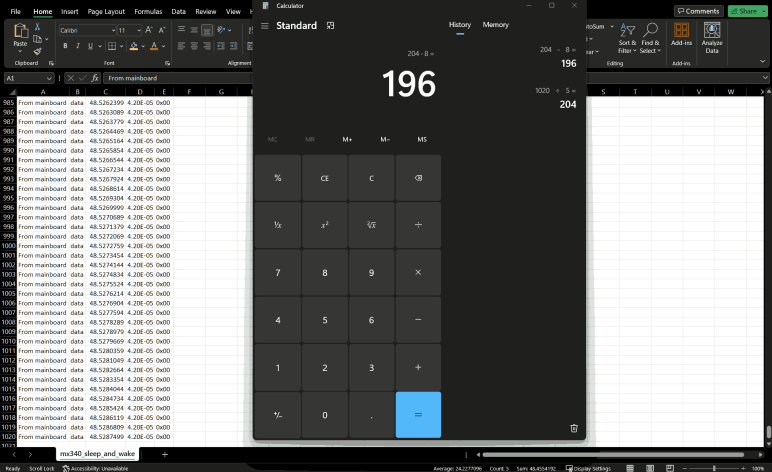
I exported the capture data for LCD screen sleep and wake, because I now recognize the sleep and wake commands. Removing them leaves just the bytes for a single screen update. I scroll down to the bottom of the spreadsheet and saw there were 1020 rows. Earlier examination found a screen update is sent in five chunks. So 1020/5 = 204 bytes per chunk. Each chunk starts with a command sequence of four 2-byte commands. 204-8 = 196 bytes of data per chunk. 196 can be factored a number of different ways: 2*98, 4*49, 7*28, or 14 squared. None of those possibilities immediately jumped out at me.
I’ve been examining the internal communication of a Canon Pixma MX340 multi-function inkjet, between its main board and its control panel. After examining what happens when the system goes into standby, I have one more trace from my initial batch of captures: a relatively simple “screen saver” mode.
Once the system is brought out of stand by and turned on, it will wait for the user to do something. If no user actions are taken, a few things happen. After just a few seconds of inactivity, it does something mechanical with the print carriage. It’s on my to-do list to better understand that later. A few minutes after that, the LCD screen goes blank. This is different from a full system standby, because the rest of the printer remains powered on. (The power LED and WiFi LEDs are still glowing, for example.) I wanted to catch this transition and see if there are any similarities to the full standby sequence.
When the LCD went blank, my logic analyzer captured a single two-byte sequence 0x04 0x75. This was very short! And very good news, because that left no ambiguity. 0x04 0x75 was indeed part of the system standby sequence, and now I have definitive proof it is a “go to sleep” command.
With the screen deactivated, I pressed a button and saw the button matrix reporting value change. Approximately 40ms after the report with new value, I saw 0x04 0xF5. 4.5ms after that, I see the LCD screen update data burst pattern. Looks like 0x04 0xF5 is a “wake up” command. Going back to review the system power-up sequence, I see 0x04 0xF5 was sent after the first LCD screen update pattern. At first I was disappointed because it contradicted the “wake up” observation, but then I remembered the first LCD screen update only lasted about 100ms before the second burst of screen data. Too short to represent data expected to be seen by the user. I had hypothesized that first update cleared the screen and this observation actually supports rather than contradicts the hypothesis: it makes sense for the system to send data to clear the screen, then wake up the screen for display. Ensuring the user is never presented with a screen filled with random uninitialized bits in memory.
Summary
0x04 0x75 = stop displaying frame buffer data on screen
0x04 0xF5 = begin displaying frame buffer data on screen
It’s still tentative and a tiny fraction of all the commands streaming across this channel, but I’m pretty happy I managed to decipher this much. It exceeded my expectation when I started this teardown project. I’m learning as I go! The next step will be to figure out what tools will help me gain further insight into this data, and I don’t think a custom Saleae Logic extension will help here.
I’m looking over data sent between control panel and main board of a Canon Pixma MX340 multi-function inkjet, and there were many mystery bytes sent during its power-up sequence. I hoped there wouldn’t be as many new things in the process of going from “On” to “Standby”.
Pressing the power button itself is absent from this logic analyzer capture file, because the power button is wired directly to the main board and not part of the button matrix reported every 9.2ms. But I could see activity in response. All transmission from the main board was acknowledged with 0x20 from the control panel, who also continued sending button matrix status every 9.2ms until the chip was put into standby.
0x0E 0xFD
(4ms)
LCD screen update to show the user “Ending…”
(2136ms)
0x0E 0xFD
(27ms)
0x04 0x75 and 0x04 0xB4.
(59ms)
0x04 0x34
(19ms)
0x04 0x14
(19ms)
0x04 0x0E
(109ms)
0x04 0xEE and 0x0E 0xDC
Chip enable pin drops to ground, putting the control panel’s NEC K13988 chip to sleep.
Comparing these bytes against what I’ve seen to date, I noticed 0x0E 0xFD shows up a lot. It was among the initialization sequence when the chip is powered up from standby, and sent again after the initial LCD screen update. Here it is sent both before and after the screen update. Other than that, the only repeat I noticed is 0x04 0x34. It was the final element in the power-up initialization burst of 13 two-byte sequences. However, none of its adjacent neighbors showed up again here.
I didn’t expect to find much commonality between powering up and shutting down. If something does show up in both (0x0E 0xFD), I will tentatively infer its purpose as more general than these specific events. Other than that, I really couldn’t draw much in the way of conclusions on what these bytes mean. I expected this kind of frustration when I started this project, but it still doesn’t feel great. Fortunately, I have an easier one to help make me feel a little better: the LCD “screen saver” blank state.
I’m using my Saleae Logic 8 logic analyzer to examine internal communication of a Canon Pixma MX340 multi-function inkjet. When the user plugs in the power cord, there was a tiny bit of internal activity even though nothing is visible to the user. I will now compare that against the communication traffic triggered by a user press on the power button.
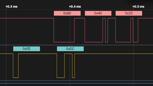
I had hoped to see some of the same things I saw during power cord plug-in happen during turn on as well, as that would reinforce the observation they are critical to startup. Indeed, roughly 15ms after enable pin was raised, there was a two-byte report of 0x80 0x40 again. This makes me confident we can look for that as the control panel’s first “I’m awake!” response after being enabled.
About 9.2ms later (another match from earlier observations) another 0x80 0x40 was reported. But it started just after the main board sent its own two-byte sequence 0xFE 0xDC. During plug-in I saw the main board send the same 0xFE 0xDC sequence, but in that case it didn’t start until just after the second 0x80 0x40 report from the control panel. Conclusion: Timing of 0xFE 0xDC is not dependent on control panel’s second report.
Since this 0xFE 0xDC transmission caught the control panel while it was in the middle of making its second 0x80 0x40 report, it appended its 0x20 acknowledgement immediately afterwards. Conclusion: the main board would not be confused if its 0xFE 0xDC transmission is immediately followed by a 0x40, it is still valid to send 0x20 acknowledgement afterwards.
After that exchange, there were twelve two-byte transmissions from the main board to the control panel, each acknowledged with a 0x20.
Main board to control panel
Control panel acknowledgement
0x0E 0xFD
0x20
0x0D 0x3F
0x20
0x0C 0xE1
0x20
0x07 0xA1
0x20
0x03 0x00
0x20
0x01 0x00
0x20
0x0E 0xFC
0x20
0x04 0xD5
0x20
0x04 0x85
0x20
0x04 0x03
0x20
0x04 0xC5
0x20
0x04 0x34
0x20
Given that the control panel just woke up, these bytes probably set configuration registers on the NEC K13988 chip. I don’t know what they all do, but the first observable effect is in the reporting data sent by the control panel every 9.2ms. Before this exchange, it would send two bytes 0x80 0x40. After this exchange, it dropped the second byte and sent just 0x80. Two such reports were sent before the next main board transmission, 0x04 0x74.
20ms later, a set of four two-byte transmissions were sent.
Main board to control panel
Control panel acknowledgement
0x04 0xF4
0x20
0x04 0x44
0x20
0x04 0x81
0x20
0x04 0x04
0x20
Again I don’t know what these mean exactly, but I noticed these all started with 0x04 as their first byte. Looking at the previous sequence of twelve bytes, the final five also started with 0x04 but none of the second bytes repeated.
After that, all was quite for about 109ms, just the regular report of 0x80 from the control panel every 9.2ms. Then the main board sent one more two-byte sequence: 0x04 0x42. After that was acknowledged, I saw a pattern I recognized: a blast of bytes to update LCD screen content starting with 0x04 0x4D, 0x04 0xC8, etc. After the sequence completed, there was one more two-byte sequence I hadn’t seen before: 0x04 0xF5. Adding to the pile of unknowns: why did this screen update needed a 0x04 0x42 preamble and 0x04 0xF5 appendix?
Another 112ms later, the main board sent 0x0E 0xFD.
Another 19ms after that, there was another blast of LCD screen content. This time, there were no 0x04 0x42 preamble, nor 0x04 0xF5 suffix.
It was a relatively long wait of 669ms until the next main board transmission: 0x0E 0xFF acknowledged with 0x20. 145us later, 0x0E 0xFF was sent again and acknowledged again. More unknowns: Why did this need to be sent twice in rapid succession?
Whatever its purpose, another LCD screen update followed 65ms later. No preamble for this one, but it was followed by 0x0E 0xFF yet again.
An even longer 1695ms (1.7 seconds) later, there was another LCD screen update transmission. This had had no extra prefix or extra suffix and, after this transmission completed, I saw only the 9.2ms button matrix report for several seconds. I stopped the capture and trimmed the data to end after this transmission.
Summary
When the user presses the power button, there were a little over three seconds of activity of data sent by the main board, each acknowledged by the control panel with 0x20:
(24ms)
13 two-byte sequences.
(17ms)
0x04 0x74
(20ms)
4 two-byte sequences.
(109ms)
0x04 0x42
LCD screen update
0x04 0xF5
(112ms)
0x0E 0xFD
(19ms)
LCD screen update
(669ms)
0x0E 0xFF twice
(65ms)
LCD screen update
0x0E 0xFF
(1695ms)
LCD screen update
(steady state)
There are four LCD screen update sequences in this capture, but the user only sees three distinct display updates. Given there was only 115ms between the first and second update, that first update didn’t stay on screen long enough to convey any useful information for human eyes. Hypothesis: the first update is a “clear screen” sequence, something to investigate later. Right now I want to look at the mirror transition of dropping from powered-on to standby.
I’ve taken a first look at control panel LCD screen update data transmission for a Canon Pixma MX340 multi-function inkjet. The bursts of data are too much for me to digest just yet, I’ll revisit that challenge later. For now, I will look at data transmission through some of this machine’s other state transitions.
I might as well start at the beginning and look at what happens when I first plug the power cable into the machine. There’s a short burst of activity (not visible to the user) before it goes into a standby state. Roughly 15ms after the chip enable signal (cyan channel 3 above) the control panel reported two bytes: 0x80 and 0x40. I’ve established 0x80 as the button matrix “no buttons pressed” report, leaving 0x40 as the mystery unknown.
When sitting in powered on steady state, button matrix reports are sent every ~9.2ms. That happens here as well: another 0x80 0x40 sequence was sent ~9.2ms after the first. After the second report, the main board responds with two bytes: 0xFE 0xDC, meaning of which is unclear for now. The control panel responds with 0x20, which I’ve seen as an acknowledgement in other trace contexts.
It appears in this initial startup state, the control panel NEC K13988 chip sends two bytes in its report. The 0x80 (no buttons pressed) and 0x40 (??). Somewhere along the line, that second byte is no longer sent as part of its regular ~9.2ms report. It might be the 0xFE 0xDC byte sequence I saw here, but I will need more data to puzzle out what’s going on.
Less than 0.1ms after the acknowledgement 0x20 was transmitted, the chip enable pin drops to ground and there’s no further activity until the machine is brought out of stand by and turned on.
Listening in to serial communication between circuit boards of a Canon Pixma MX340 multi-function inkjet, I think I have a handle on how the control panel reports button presses to the main board. Some of these button presses trigger updates to information shown on the control panel LCD screen, which gave me a first look at what that involved.
Pressing right/+ button at the home screen incremented a number on screen representing number of copies to be made. Pressing left/- afterwards triggered another update as the number was decremented. For each of the two screen updates, I observed similar behavior. It starts with four two-byte sequences from the mainboard, each followed by a single byte 0x20 from the control panel which is probably an “OK” acknowledgement.
After that, a large number of bytes were sent from the mainboard. I didn’t find a way to ask Saleae Logic to count the number of bytes for me. (I hope I don’t end up counting manually) But at least it was easy to measure the time interval for this transmission: 14ms. At 250000 baud 8E1, that can’t be more than (0.014 seconds * 250000 symbols per second / 11 symbols per byte) = 318 bytes. Plus I saw a few pauses in between this data transmission, so it wasn’t transmitting at full speed. Looking at powers of two numbers, I think 256 bytes is a good candidate. At the end of this burst of bytes, there was another 0x20 acknowledgement from the control panel.
[UPDATE: I’ve figured out the burst is 196 bytes long, shorter than the 256 I guessed. 196 decimal is 0xC4 hexadecimal, which explains the fourth two-byte transmission. 0x06 0xC4 must mean “I am about to send you 196 bytes”]
This pattern (four two-byte sequences, followed by a large number of bytes) was repeated five times.
Transmission from main board
Acknowledgement by control panel
0x04 0x4D
0x20
0x04 0xC8
0x20
0x04 0x30
0x20
0x06 0xC4
0x20
[… 196 bytes …]
0x20
0x04 0xCD
0x20
0x04 0xC8
0x20
0x04 0x30
0x20
0x06 0xC4
0x20
[… 196 bytes …]
0x20
0x04 0x2D
0x20
0x04 0xC8
0x20
0x04 0x30
0x20
0x06 0xC4
0x20
[… 196 bytes …]
0x20
0x04 0xAD
0x20
0x04 0xC8
0x20
0x04 0x30
0x20
0x06 0xC4
0x20
[… 196 bytes …]
0x20
0x04 0x6D
0x20
0x04 0xC8
0x20
0x04 0x30
0x20
0x06 0xC4
0x20
[… 196 bytes …]
0x20
Looking at the four two-byte sequences, they differed only in the second byte of the first pair. I’ve highlighted this byte in the table above. Perhaps this is an address of some sort, and if so I find it interesting the values are not consecutive from one iteration to the next.
I haven’t figured out how I’ll analyze the burst of data. A few hundred bytes is too unwieldy to examine in a linear capture timeline, I’ll have to think about what other tools I could bring in. [UPDATE: Microsoft Excel to the rescue.] Despite that open question, this established a baseline pattern for comparison against other machine states.
I have my Saleae Logic 8 logic analyzer set up to listen in on the communication between control panel and main board of a Canon Pixma MX340 multi-function inkjet. After picking a few scenarios to record, I decided to start by looking at its steady-state behavior. I expect this to provide a baseline I can compare against for examining state change behaviors. I think I can get my baseline behavior from the trace where I pressed four buttons, as there should be plenty of steady-state information between my button presses.
Here’s a snapshot of steady-state behavior under the oscilloscope. Channel 1 (yellow, main board to control panel) is held high, transmitting no data. Channel 3 (cyan, control panel enable) is held high to keep the K13988 chip active. The only activity here is on channel 2 (magenta, control panel to main board) where a short burst of activity occurs every 9+ milliseconds.
Zooming in, it looks like a simple square wave.
When interpreted as 250000 baud 8E1 serial data, this pulse represents a single byte of data with value of 0x80. Saleae Logic software measured interval of these pulses at 9.2ms apart, and a different value is conveyed if a button is pressed.
Button Pressed
Value reported every 9.2ms (Hexadecimal)
(None)
0x80
OK
0xC9
Right/+
0xCA
Left/-
0xCB
Back
0x93
Looking at these values, I noticed “OK”, “Right/+” and “Left/-” generated consecutive values, but “Back” was very different. Looking at the button matrix I mapped out earlier, I see the three consecutive values were all associated with pin 1. This increases my confidence in my button matrix, and this reported value is probably the button’s position in that matrix.
This button matrix state is sent every 9.2ms, even if there’s additional communication between the main board and control panel. For example, during the ~70ms required to update information displayed on the LCD screen, button matrix state is still sent in between all the display data acknowledgements.
My Saleae Logic 8 logic analyzer has tapped into the communication lines between main board and control panel of a Canon Pixma MX340 multi-function inkjet. The asynchronous serial data decoder is now configured to 250000 baud 8E1 to match. (Or if it’s not 250000 baud, it’s at least close enough.) It’s time to get some data to analyze!
First I started with power cycle scenarios:
Plug in the power cable, watching the power-up sequence transitioning to standby state. From earlier oscilloscope traces I know the NEC K13988 chip on the control panel is briefly enabled by the mainboard. This should be a relatively short sequence to analyze, and hopefully enough to understand the minimum required sequence to start the K13988. There is no visible activity on the LCD screen during this sequence so that’s not expected to be part of this picture.
Push the power button, watch transition from standby to on. This enables the K13988 and displays several different things on the LCD screen in rapid succession. I expect to see the K13988 initialization again, plus a lot more to initialize the rest of the control panel. There should be a LCD initialization sequence here, and several screen frame buffer updates. This is expected to be the longest and most complex sequence to analyze.
Push the power button again, watch transition from on to standby. This should be a slightly shorter sequence. There’s one LCD screen update to show “Ending…” as the printer goes to standby, then the screen and K13988 drops off to sleep.
Then I added the following scenarios:
While in on state and at the home menu, I pushed four buttons in sequence: “OK”, which gave me an error beep and no screen update. “Right”, which did trigger a screen update, incrementing the number of copies. “Left”, which was another update decrementing the number. Finally “Back”, which is again an error beep and no screen update. This gives me activity for four different button presses, two of which triggered screen updates but two did not.
While in on state and at the home menu, I left the machine alone until it put the LCD screen to sleep. Then I pushed a button to wake the screen back up. This capture should have the commands to deactivate the LCD while still keep K13988 active, followed by commands to wake up the LCD. I will be curious to see if a full LCD screen update frame buffer is sent as well.
While in standby state, I lifted the scanner imaging head off of its track then pushed the power button. This will cause a failure of its homing sequence and trigger an error display screen, toggling LCD text between “Printer error has occurred” and “5011”. Capturing this sequence will show LCD screen update without any noise from user input.
If anyone else is curious, these logic analyzer capture files are up on my GitHub. As a first pass, I don’t expect the these captures to answer all the questions I have. Heck, I’m not even confident they’ll make sense. But I can always come back to capture different activity. For now, they’re good enough to serve as a starting point and establish a baseline.
Using an oscilloscope, I looked at the communication between the main board and control panel of a Canon Pixma MX340 multi-function inkjet. I’ve tentatively identified the communication protocol as asynchronous serial. Manually decoding the waveform, it looks like eight data bits are followed by an even parity bit and a stop bit, a configuration represented by shorthand 8E1. The transmission speed is roughly double that of common speed 115200 baud, so in the neighborhood of 230400 baud. This is enough of a starting point for me to hand off decoding duties to my Saleae Logic 8 (*).
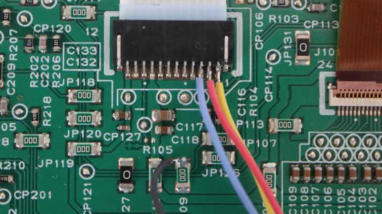
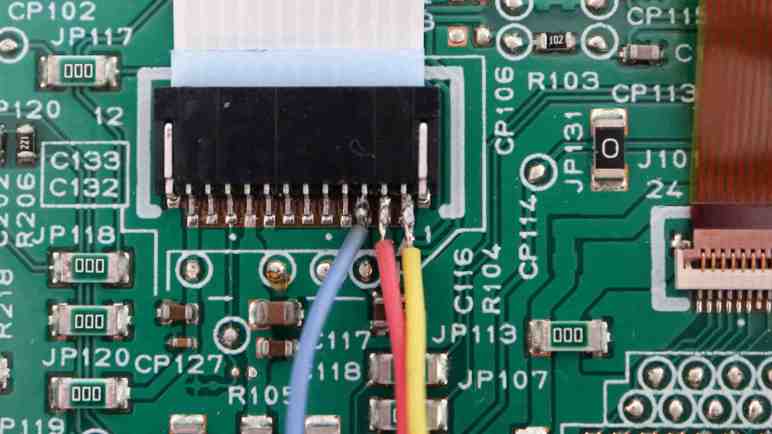
The logic analyzer came with two sets of wires, four channel per set. It also came with tiny springy gripper probes designed to hook onto thin wire and/or IC legs. They work well but for this project I expect to flip the control panel over frequently. Switching between pushing buttons in the front and probing its circuit in the back. Small spring-loaded clips won’t be reliable as I move the circuit board around, so I’ll crimp my own connectors to wires that I will solder directly to the circuit board. This was pretty easy because Saleae designed the Logic 8 with standard 0.1″ spacing connectors. Letting me use stuff I bought for earlier projects. I pulled out my assortment of 0.1″ connectors (*) that included the 2×4 type I need for this project, a crimping tool I would recommend (*) and spools of thin 30-gauge wire with flexible silicone insulation. (*)
I followed color precedence set by Saleae’s wiring, because that color coding carries into their Logic 8 software and I didn’t want to get confused by color mismatches. This makes for a pretty odd subset but should be fine for my purposes. I only connected a single ground wire, thinking that should be sufficient for this project. I can put in more later if I’m wrong.
I copied the color scheme used with my oscilloscope probes, so again the color stays consistent in my brain. Yellow = main board to control panel. Red = control panel to main board. Blue = chip enable. The biggest difference is that the oscilloscope probes had an alligator clip I could attach to the metal chassis for ground. Here I had to solder the ground wire. Instead of fussing with the 1mm pitch connector, I soldered the ground wire to one of the zero ohm resistors serving as jumper. (JP109)
Setting Saleae protocol analyzer to decode serial data at 230400 baud 8E1 resulted in parity and frame errors. Zooming in to one such error, I saw the analyzer helpfully plotted dots where it sampled data bits. The misalignment between those dots and data pulses told me 230400 was the wrong baud rate. These samples also provided timing information between high-low and low-high transitions, giving me a range of times from 3.9us to 4.1us. Going with 4us as the intent gives 1000000/4 = 250000 baud.
I have never encountered baud rate of 250000 before, but that’s what seems to makes sense to my logic analyzer. It might still be a touch off… that parity bit at the end is slightly off center of the associated bit. Maybe it’s 249000 baud? I can fine-tune as I go. It’s not a common baud rate but Canon engineers didn’t have to use a common baud rate. Canon made both the main board and control panel, they can use whatever baud rate they want. What data is getting transmitted? Well, that’s what I’m going to try to find out starting with a few select samples.
I’ve got the control panel of a Canon Pixma MX340 multi-function inkjet on my workbench, hooked up to my oscilloscope. I’ve located the three wires used for communication between the main board and the control panel circuit board. Monitoring activity of these three wires with my oscilloscope, two of the pins are behaving as communication lines one in each direction and the third has been tentatively identified as a Chip Enable signal for the NEC K13988 chip on board the control panel circuit board.
Before oscilloscope observation, I didn’t know what those three wires were. I thought the best guess was SPI with clock, MOSI, and MISO. I felt I2C was less likely due to its official design intent of communication on the same circuit board, it’s not as robust for running across long ribbon cables. But since I saw no clock signal on any of these three wires, synchronous protocol like SPI and I2C are ruled out. I don’t know any asynchronous protocols aside from old school serial, so I hoped that was it. I went back to my first tutorial of asynchronous serial published by Sparkfun for comparison against my set of oscilloscope traces.
Here was the transmission from control panel to main board, reporting the press of “Back” button. (Leftmost of four buttons under the LCD screen.) Horizontal scale is 5us per grid here, and each state is held for less than one grid. Five of them seem to fit nicely in four grids, so call it 4us per bit. If I interpret this graph as serial data, I would get: 0 for the start bit, 11001001 for 8 data bits, 0 would represent an even parity bit, and a final 1 bit as stop bit. This is consistent with serial. Repeating the exercise with my remaining button press traces, they all had patterns that made sense as 8E1 serial data.
As for the speed, 115200 baud is pretty common for microcontroller projects I’ve examined. 1/115200 = 8.68us, about double the time for each of these bits, implying this is double that speed in the neighborhood 115200 * 2 = 230400 baud. So I will try interpreting this data as 8E1 serial data at 230400 baud and see how far I get.
I have hooked up my oscilloscope to the control panel circuit board of a Canon MX340 multi-function inkjet, watching communication between the inkjet main board and the control panel. Updating information shown on the LCD screen involved too much data for me to decipher on the oscilloscope, far more than the amount of data reporting button status. But there’s one more communication wire between the main board and control panel, with comparatively little activity. I think this third wire is “Chip Enable” for a NEC K13988 chip on the control panel.
Here’s an oscilloscope capture of the first second and a half after I plugged the printer in. There was a bit of activity on all three communication wires in the final 100ms of this chart.
Zooming in, channel 1 (yellow line) has been established as the wire used by the mainboard to send LCD screen updates. It makes sense for the main board wire to be the first to rise up to 3.3V and the last to fall in this sequence. Channels 2 and 3 came up to 3.3V together and shortly after that, channel 2 showed a pulse representing data sent from K13988 to main board. After that, things go quiet again.
But “2 and 3 together” is not literally simultaneous. Zooming much further in, I can see channel 3 started rising first and channel 2 didn’t start rising until after channel 3 rose above 1.6V. A similar thing happens when the printer wakes up out of stand by.
On the other end of the process, here’s a trace when the printer goes into standby. A few bytes of data were communicated between the main board and the K13988. Then channel 3 drops to ground, followed by channel 2 dropping to 2.5V.
All of the above activity are consistent with a “Chip Enable” signal on channel 3. Upon plugging in the printer, the main board wakes up the control panel’s NEC K13988 chip. After hearing acknowledgement data from the K13988, the main board drops it off to sleep. When the user presses the power button to bring the system out of standby, pin 3 wakes up the NEC K13988 and stays at 3.3V DC until time to go to sleep again.
I’ve been looking at the control panel circuit board from a Canon Pixma MX340 multi-function inkjet. I have found the pins used for communication between the main board and control panel, and connected them to my oscilloscope. The first discovery was the line used by the control board to report button status back to the main board.
Here is a sample of communication activity on that line, reporting the user has pressed the “OK” button. (Rightmost of four buttons below the LCD screen.)
When I press a button that is not valid for the current menu, I hear an error beep. In this error case, information on the LCD does not change and nothing happens on pin 1 (yellow line). But if I press a valid button causing a change on screen, I see a digital serial communication wave form on the oscilloscope screen. A lot more of it.
I had to zoom out to get an idea of how much more. Whatever it is, it takes around 72ms to complete. Notably, it takes the same amount of time no matter what changed on screen. It doesn’t matter if I change only a single digit or navigate to an entirely different menu. If there’s any change, there will be ~72ms of activity on pin 1. This puts an upper limit on screen refresh rate of (1000/72) = 13.89 frames per second. Too slow for video games (no Doom for this screen) but perfectly fine for an inkjet control panel.
Transmission time of ~72ms would cover multiple cycles of pin 2 keyboard update data. This means keyboard status could change in the middle of a screen update, though again this lack of responsiveness is not a concern for an inkjet control panel.
To try to get some context as to the magnitude of data involved here, I went back to looking at data on pin 2. It looks like each bit takes roughly 4us to transmit. A millisecond would allow 1000/4=250 bits to be transmitted. 250 bits * 72 milliseconds = 18,000 bits. I look at the LCD and it looks like each character is represented by 8×16 pixels and there’s room for two lines of 28 characters each. 8*16*2*28 = 7168 which is less than half of that wild guess.
That was only a rough estimate. Screen update data isn’t necessarily transmitted at the same rate as keyboard data. Some of that data will be transmission overhead, so on and so forth. But getting the rough magnitude is informative for some broad strokes. If refreshing the entire screen took very little data, I could infer the mainboard is probably sending ASCII character values. But the quantity involved here meant the main board is probably not doing that. There’s more than enough to be transmitting the entire LCD screen frame buffer as a raw bitmap. It also meant manually decoding this data on my oscilloscope is a hopeless task. Thankfully, I now have tools to help tackle such things. Before I do, though, there’s still one more wire to examine under the oscilloscope.
The control panel of a Canon Pixma MX340 multi-function inkjet has only one significant microchip. It is marked NEC K13988 and I’ve traced through how it is connected to the rest of the circuit board. Among these connections are two communication channels. One to the main board, and one to the LCD screen. I decided to look at main board communication first, wiring up those three pins to see how it looks under my Siglent oscilloscope. Since they were pins 1-3 on the circuit board connector, it was easiest to wire them up to channels 1-3 on the oscilloscope.
I saw a little bit of activity when I plugged in the printer, before I turned it on. Pin 2 came up to about 2.5V DC, and pin 1 came up just a little higher for 300ms before dropping back. About one second later, pin 1 came up to 3.3V, followed a few tens of milliseconds later by pins 2 and 3 together. A few tens of milliseconds after that, pin 3 dropped to ground and pin 2 dropped to 2.5V at around the same time. Then pin 1 dropped to ground, and all three lines stayed that way (pin 1+3 ground, pin 2 at 2.5V DC) for the printer standby state.
When I pressed the power button to turn on the printer, there was a flurry of activity I don’t understand yet, but it quickly settled to this state:
This is what it looks like when the printer is on with data on the LCD screen, but nothing else happening. Pins 1 and 3 stay at 3.3V DC with no activity. Pin 2 (magenta line) sends something at regular intervals. A little over 9ms between pulses, or at the oscilloscope measured rate at 108.439Hz.
Zooming in on the pin 2 state, it looks like it dips to ground for about 33us.
Pressing a button triggers a change on pin 2 activity. For this exploration I tried the four buttons under the LCD screen, starting with the above trace representing the back button.
Pressing left arrow/- generated trace above.
Pressing right arrow/+.
And pressing OK.
These snapshots make pin 2 look like a digital serial communication data stream describing user input to the main board. It’s a short enough burst I can probably decode the values by hand [UPDATE: I decoded them by hand.] but right now I want to look at other pins first.
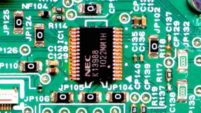
I’m looking at a Canon Pixma MX340 multi-function inkjet’s control panel circuit board, and I’m slowly peeling back the curtain on its implementation details. After tracing through the circuitry to label every pin on the connector for communicating with the main board, I turned my attention to the biggest component on the board: a 30-pin chip marked with NEC K13988. I didn’t have any luck finding an official datasheet describing this chip so I have to infer its functionality by how it is connected to everything else on the circuit board.
Starting with the just-deciphered main board connector, I found three wires connected to K13988 which probably meant some sort of digital serial data communication. (Data, Clock, and…?) K13988 also communicates with the LCD screen with five wires, but I don’t have a good candidate on 5-wire protocols. I’ll look at that later.
Also provided by the main board are power and ground. The power line is relatively straightforward, but there were several K13988 pins indirectly going to ground via a component labeled NF104. NF104 is tiny and lack markings other than the NF104 label. I believe Canon engineers would have used common prefix if it was a resistor (R), a capacitor (C), or a fuse (F). I don’t know what the NF prefix means and it’s not on Wikipedia’s list of common reference designation prefix.
Two pins control LEDs indicating WiFi and Memory/In Use. Two pins go to a component X1. I associate the form factor with crystal oscillators, and this one was marked with 6.1AKSSOHT. I don’t know how to interpret that in terms of an oscillator frequency.
Eleven pins are wired to a matrix of buttons. Tracing them took me all around the circuit board. I lost track several times and unknowingly jumped to a different trace, leading to conclusions that made no sense and had to be redone. It took a few tries to generate this table. Accuracy is still dubious, but it is at least consistent and plausible. I’m not sure if convention is to call this 4 rows and 7 columns, or 7 rows and 4 columns. They read status of 27 buttons not under direct main board control. (One short of maximum possible combination of 7*4=28 buttons.) I color-coded them in this table, but I’m not sure if that actually makes it any more readable. The ordering of buttons in this list corresponds to the order in which the copper traces visited them, starting from the K13988. Example: starting from K13988 pin 1, following that trace will reach SW220 first, then SW213, then SW207, and finally SW227.
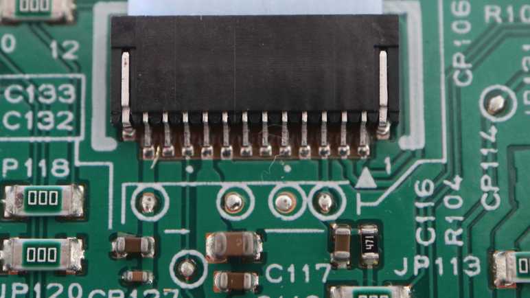
There was no shortage of surprises as I’m learning from the control panel circuit board of a Canon Pixma MX340 multi-function inkjet. I followed a wire that I thought supplied power to multiple components, found it powered just a single LED, then realizing the LED on/off is actually controlled by a transistor further down the line. Weird! Fortunately the remaining pins on this connector (for ribbon cable to main board) were easier to understand, enough for me to generate a medium-confidence pinout chart.
Connector to main board pin 11 was soldered to a trace that went under the connector and out the top side. Tracing its path through a zero-ohm jumper resistor (JP117), a few check points (CP102, CP112), an unpopulated capacitor position (C110) and a 220 ohm resistor (R101) I arrived at the “Stop” button (SW101) at the control panel’s far right edge. Canon engineers decided a user trying to stop something in a panic should have a direct line to the main board bypassing the NEC K13988 intermediary.
Connector to main board pin 3 was connected to a capacitor (C116) to ground typical of a decoupling capacitor, and a 470 ohm resistor (R104) typical for LED current limiting. Upon initial examination I thought it might lead to one of the LEDs, but I’ve accounted for all LEDs by now so I know it isn’t that. I traced its route through CP114 and CP126 to arrive at K13988 pin 29.
Connector to main board pin 2 and pin 1 traveled side-by-side, but received slightly different treatments. Pin 2 signal had to travel through a 100 ohm resistor (R103) while pin 1 signal did not. Pin 2 also had a capacitor (C115) to ground while the pin 1 equivalent position (C114) is unpopulated. When they reached the K13988 chip, main board connector pin 1 signal went to K13988 pin 16, and main board pin 2 went to K13988 pin 18.
Pin numbering is right-to-left in the picture, as per arrow and number 1 printed adjacent to the right end of the connector. There is also a dot every 5 pins to aid in counting. After tracking down all of these traces, I repeated the exercise with pins connected to the K13988 chip.
I’m examining the control panel of a Canon Pixma MX340 multi-function inkjet, and I found an interesting mix. Most of the buttons and such are managed by a NEC K13988 chip on the circuit board, but a few select items like the power button and nearby LEDs have direct connections to the main board.
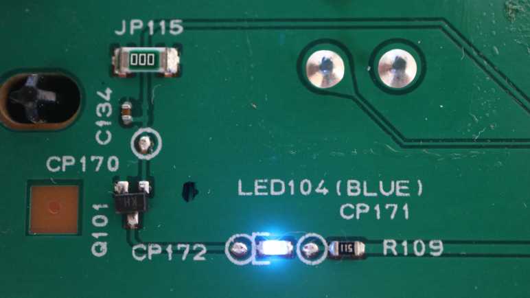
That discovery meant I’ve got most of the main board connector pins identified, and I thought I’d finish the job. Starting with pin 12, furthest away from the K13988 chip. On my first pass I identified it as a 5.5V DC power supply, and I was curious what needed the burly power of a nice thick copper trace. I followed it down and left to a bright blue LED.
Well, technically it went to a 510 ohm resistor (R109) and check point (CP171) before reaching LED104. This LED shines into a clear plastic light guide to illuminate the “WiFi” sign on the front panel. Since I’ve established the WiFi module is connected to the main board, I thought it made sense the main board would control whether this WiFi sign is lit. But that’s not what’s going on here! The circuit continues through another check point (CP172) to a transistor (Q101) that controls whether or not to connect the other end of the LED to ground. The control signal voltage travels through a check point (CP170), buffered with a capacitor (C134) and circles back into the heart of the circuit board. I followed it all the way back to pin 2 of K13988.
This is very curious, because it implies the K13988 is responsible for turning this LED on or off by controlling the transistor. If that’s the whole picture, it wouldn’t have been terribly difficult to replace R109 with a lower resistance value and connect it to the 3.3V DC power plane that already existed on this board. I found no other branches for the 5.5V line, so there must have been a reason why they ran a separate 5.5V DC wire on the ribbon cable just for this LED. Does this LED draw too much power for the existing 3.3V DC power plane? Maybe the main board reserves the ability to turn it off by cutting power?
This project to trace main board connector pin 12 actually raised more questions than it answered. Fortunately there weren’t too many other mysteries attached to remaining main board connector pins.
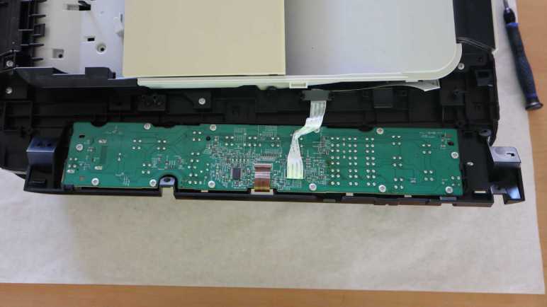
I’m exploring the control panel from a Canon Pixma MX340 multi-function inkjet. To help navigate my journey, I took multiple close-up photos of copper traces on the circuit board and stitched them together. With my new detailed atlas in hand, my first journey is the power button and nearby LEDs.
Mechanically, the control panel is built from multiple layers of injection-molded plastic. Here is the second layer that bridges between facade in front and circuit board behind.
Pre-built buttons with integrated LED exist, but Canon didn’t use one here. They made their own using a custom clear plastic piece serving as both light guide and the thing user actually pushes. On the circuit board it’s a standard button with an adjacent standard LED.
That’s all great, but the focus today is tracing their circuit on the back. I inferred the NEC K13988 chip is responsible for reading most buttons on this control panel, but I thought a few critical items likely bypassed the NEC chip and are routed directly to the main board ribbon cable. The power button is a great candidate: routing that directly to the main board gives Canon the option of powering down the NEC K13988 chip while in standby mode.
The power button has four legs. Two of them are soldered to the ground plane, and a third has its own island not connected to anything else. That leaves a single signal wire that travels across half the circuit board. Near the mainboard connector, it meets up with resistor labeled R100 and marked with 221 (220 ohms), then continued on to main board pin 7. Hypothesis confirmed!
Adjacent to the power button is the power LED, and again one leg is soldered to ground. The other leg goes to check point CP142, unpopulated capacitor C119, and resistor R110 marked 101 (100 ohms) then traveled alongside the power button trace all the way to main board pin 6. Since the main board is responsible for the power button, it made sense it also has control of power LED.
The “Alarm” LED is set up much the same way: one leg to ground, other leg to check point CP143, unpopulated capacitor C120, and resistor R111 also marked 101 (100 ohms). Then it jumped over a trace with JP1 before meeting up with the power LED trace all the way to main board pin 5. It is no surprise the main board has direct control of the error indicator LED.
In comparison, the “In Use/Memory” LED was implemented differently. One leg taps into the always-on 3.3V DC voltage plane from main board pin 9. The other leg disappears underneath K13988. Determining exactly which K13988 pin is responsible for sinking “In Use/Memory” LED is a future exercise. Right now I have learned enough to fill in a few entries from the earlier incomplete table of main board connector pins, and I want to work towards filling in the rest.
[UPDATE: After investigation, this post has the table fully filled in.]