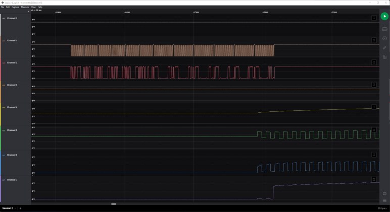
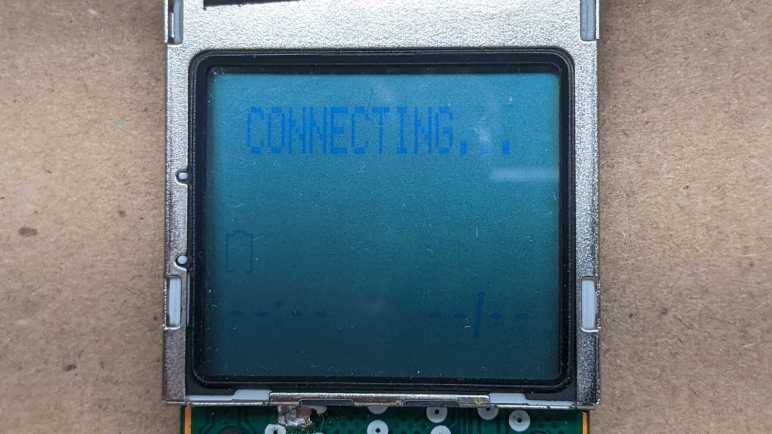
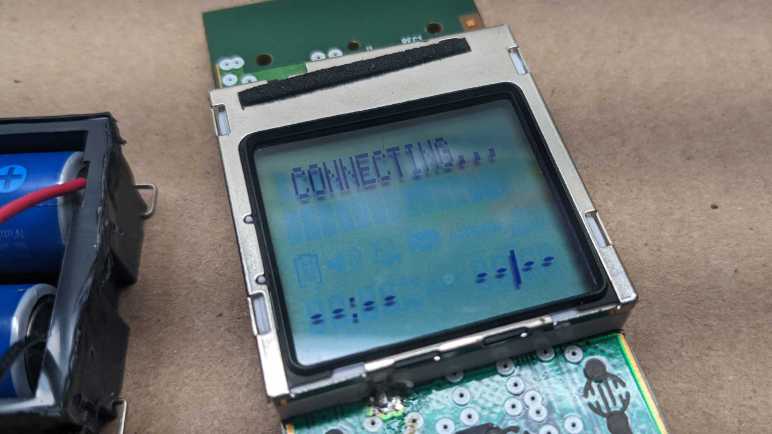
I’ve been examining the internal data communication of a Canon Pixma MX340 multi-function inkjet, trying to understand the data sent between its system main board and its control panel. Out of all the data sequences I’ve captured and analyzed, the LCD “screen saver” deactivation/reactivation sequence was the easiest to understand. Others were more difficult, though I still think I’ve picked up bits and pieces. Enough to form a foundation from which to make more detailed observations.
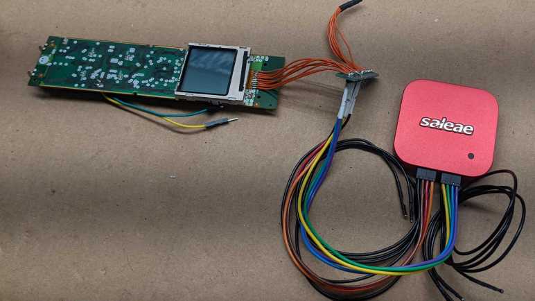
But how would I go about such observations? There’s enough data involved that scrolling through the timeline of my Saleae Logic 8 analyzer software and decoding things manually is not practical. I need to bring additional tools into the problem. This is not an unusual task and Saleae has some provisions for users to parse and understand data captured by their logic analyzers. It is possible to write custom extensions for their Logic 2 analyzer software, plugging in our custom processing. For my specific scenario, where I want to apply context to a stream of decoded data, the type of extension is are called High-Level Analyzer (HLA) because it sits in the processing above the low-level asynchronous serial decoder.
I like the idea of writing a bit of Python code to leverage all the infrastructure that already existed in Saleae Logic 2 software. Unfortunately, as I read into their documentation, I realized it would fall short of my needs for this specific project in two important ways.
The first shortfall is a HLA can only process data from a single channel. This means a HLA can be configured to interpret bytes from main board to control board. (“This is a burst of data to update LCD screen”.) Or it can be configured on the channel sending bytes from control board back to main board. (“This 0x80 value means no buttons are currently pressed.”) But if I want to look at both channels (“This is a LCD update, followed by a single byte 0x20 as acknowledgement sent in return”) I’m out of luck. Multi-channel HLAs are a long-standing feature request that, as of this writing, is still not available.
The second shortfall is a HLA’s output is pretty much restricted to adding text annotation on the Saleae data timeline, or logging text to the developer console. I want to be able to parse the LCD screen data into a bitmap shown on screen, and I found no such facility to do so within Saleae Logic’s Extension framework.
There must exist software tools that I can leverage to perform the analysis I want, but so far I have failed to think up the correct keywords to find them online. I may have to roll my own. In the course of researching how to do so, I expect to learn the techniques and terminologies that help me find the right software making my own project superfluous. It wouldn’t be the first time I’ve done that, but at the end I would have learned what I want. That’s what matters.
And you know what else I’ve done many times in the past? Overthinking a problem! I could get started without writing any code, by using a tool I don’t usually associate with my electronics projects: Microsoft Excel.