Canon Pixma MX340 Control Panel Data Communication: Plug In

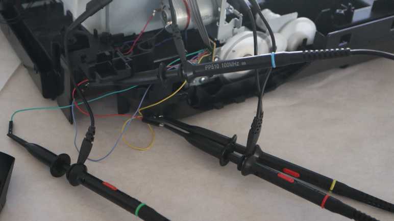
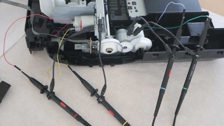
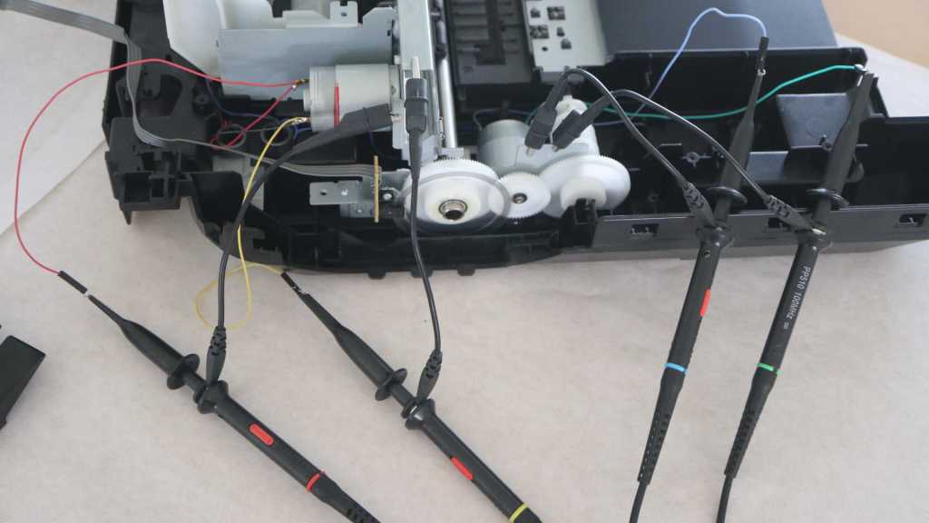
I’ve taken a first look at control panel LCD screen update data transmission for a Canon Pixma MX340 multi-function inkjet. The bursts of data are too much for me to digest just yet, I’ll revisit that challenge later. For now, I will look at data transmission through some of this machine’s other state transitions.

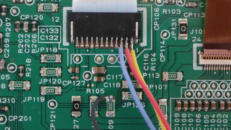
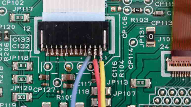
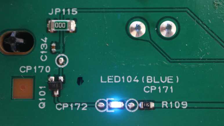
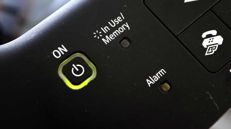
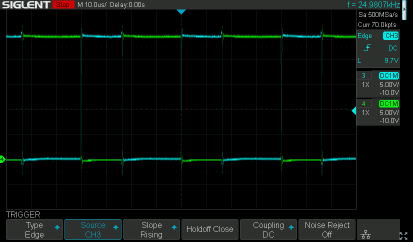
I might as well start at the beginning and look at what happens when I first plug the power cable into the machine. There’s a short burst of activity (not visible to the user) before it goes into a standby state. Roughly 15ms after the chip enable signal (cyan channel 3 above) the control panel reported two bytes: 0x80 and 0x40. I’ve established 0x80 as the button matrix “no buttons pressed” report, leaving 0x40 as the mystery unknown.

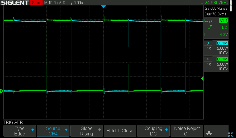
When sitting in powered on steady state, button matrix reports are sent every ~9.2ms. That happens here as well: another 0x80 0x40 sequence was sent ~9.2ms after the first. After the second report, the main board responds with two bytes: 0xFE 0xDC, meaning of which is unclear for now. The control panel responds with 0x20, which I’ve seen as an acknowledgement in other trace contexts.

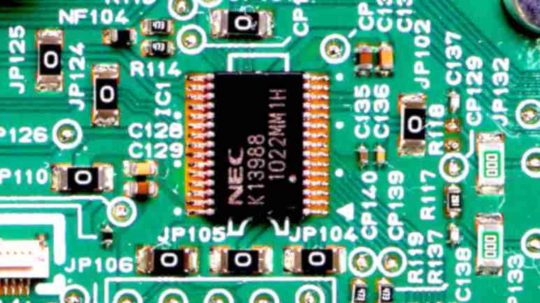
It appears in this initial startup state, the control panel NEC K13988 chip sends two bytes in its report. The 0x80 (no buttons pressed) and 0x40 (??). Somewhere along the line, that second byte is no longer sent as part of its regular ~9.2ms report. It might be the 0xFE 0xDC byte sequence I saw here, but I will need more data to puzzle out what’s going on.

Less than 0.1ms after the acknowledgement 0x20 was transmitted, the chip enable pin drops to ground and there’s no further activity until the machine is brought out of stand by and turned on.


This teardown ran far longer than I originally thought it would. Click here to rewind back to where this adventure started.

Canon Pixma MX340 Control Panel LCD Screen Update First Look

Listening in to serial communication between circuit boards of a Canon Pixma MX340 multi-function inkjet, I think I have a handle on how the control panel reports button presses to the main board. Some of these button presses trigger updates to information shown on the control panel LCD screen, which gave me a first look at what that involved.

Pressing right/+ button at the home screen incremented a number on screen representing number of copies to be made. Pressing left/- afterwards triggered another update as the number was decremented. For each of the two screen updates, I observed similar behavior. It starts with four two-byte sequences from the mainboard, each followed by a single byte 0x20 from the control panel which is probably an “OK” acknowledgement.

After that, a large number of bytes were sent from the mainboard. I didn’t find a way to ask Saleae Logic to count the number of bytes for me. (I hope I don’t end up counting manually) But at least it was easy to measure the time interval for this transmission: 14ms. At 250000 baud 8E1, that can’t be more than (0.014 seconds * 250000 symbols per second / 11 symbols per byte) = 318 bytes. Plus I saw a few pauses in between this data transmission, so it wasn’t transmitting at full speed. Looking at powers of two numbers, I think 256 bytes is a good candidate. At the end of this burst of bytes, there was another 0x20 acknowledgement from the control panel.

[UPDATE: I’ve figured out the burst is 196 bytes long, shorter than the 256 I guessed. 196 decimal is 0xC4 hexadecimal, which explains the fourth two-byte transmission. 0x06 0xC4 must mean “I am about to send you 196 bytes”]

This pattern (four two-byte sequences, followed by a large number of bytes) was repeated five times.

Transmission from main boardAcknowledgement by control panel
0x04 0x4D0x20
0x04 0xC80x20
0x04 0x300x20
0x06 0xC40x20
[… 196 bytes …]0x20
0x04 0xCD0x20
0x04 0xC80x20
0x04 0x300x20
0x06 0xC40x20
[… 196 bytes …]0x20
0x04 0x2D0x20
0x04 0xC80x20
0x04 0x300x20
0x06 0xC40x20
[… 196 bytes …]0x20
0x04 0xAD0x20
0x04 0xC80x20
0x04 0x300x20
0x06 0xC40x20
[… 196 bytes …]0x20
0x04 0x6D0x20
0x04 0xC80x20
0x04 0x300x20
0x06 0xC40x20
[… 196 bytes …]0x20

Looking at the four two-byte sequences, they differed only in the second byte of the first pair. I’ve highlighted this byte in the table above. Perhaps this is an address of some sort, and if so I find it interesting the values are not consecutive from one iteration to the next.

I haven’t figured out how I’ll analyze the burst of data. A few hundred bytes is too unwieldy to examine in a linear capture timeline, I’ll have to think about what other tools I could bring in. [UPDATE: Microsoft Excel to the rescue.] Despite that open question, this established a baseline pattern for comparison against other machine states.


This teardown ran far longer than I originally thought it would. Click here to rewind back to where this adventure started.

Canon Pixma MX340 Control Panel Button Status Report

I have my Saleae Logic 8 logic analyzer set up to listen in on the communication between control panel and main board of a Canon Pixma MX340 multi-function inkjet. After picking a few scenarios to record, I decided to start by looking at its steady-state behavior. I expect this to provide a baseline I can compare against for examining state change behaviors. I think I can get my baseline behavior from the trace where I pressed four buttons, as there should be plenty of steady-state information between my button presses.

Here’s a snapshot of steady-state behavior under the oscilloscope. Channel 1 (yellow, main board to control panel) is held high, transmitting no data. Channel 3 (cyan, control panel enable) is held high to keep the K13988 chip active. The only activity here is on channel 2 (magenta, control panel to main board) where a short burst of activity occurs every 9+ milliseconds.

Zooming in, it looks like a simple square wave.

When interpreted as 250000 baud 8E1 serial data, this pulse represents a single byte of data with value of 0x80. Saleae Logic software measured interval of these pulses at 9.2ms apart, and a different value is conveyed if a button is pressed.

Button PressedValue reported every 9.2ms
(Hexadecimal)
(None)0x80
OK0xC9
Right/+0xCA
Left/-0xCB
Back0x93

Looking at these values, I noticed “OK”, “Right/+” and “Left/-” generated consecutive values, but “Back” was very different. Looking at the button matrix I mapped out earlier, I see the three consecutive values were all associated with pin 1. This increases my confidence in my button matrix, and this reported value is probably the button’s position in that matrix.

This button matrix state is sent every 9.2ms, even if there’s additional communication between the main board and control panel. For example, during the ~70ms required to update information displayed on the LCD screen, button matrix state is still sent in between all the display data acknowledgements.


This teardown ran far longer than I originally thought it would. Click here for the starting point.

Canon Pixma MX340 Control Panel Logic Analyzer Capture Targets

My Saleae Logic 8 logic analyzer has tapped into the communication lines between main board and control panel of a Canon Pixma MX340 multi-function inkjet. The asynchronous serial data decoder is now configured to 250000 baud 8E1 to match. (Or if it’s not 250000 baud, it’s at least close enough.) It’s time to get some data to analyze!

First I started with power cycle scenarios:

  1. Plug in the power cable, watching the power-up sequence transitioning to standby state. From earlier oscilloscope traces I know the NEC K13988 chip on the control panel is briefly enabled by the mainboard. This should be a relatively short sequence to analyze, and hopefully enough to understand the minimum required sequence to start the K13988. There is no visible activity on the LCD screen during this sequence so that’s not expected to be part of this picture.
  2. Push the power button, watch transition from standby to on. This enables the K13988 and displays several different things on the LCD screen in rapid succession. I expect to see the K13988 initialization again, plus a lot more to initialize the rest of the control panel. There should be a LCD initialization sequence here, and several screen frame buffer updates. This is expected to be the longest and most complex sequence to analyze.
  3. Push the power button again, watch transition from on to standby. This should be a slightly shorter sequence. There’s one LCD screen update to show “Ending…” as the printer goes to standby, then the screen and K13988 drops off to sleep.

Then I added the following scenarios:

  1. While in on state and at the home menu, I pushed four buttons in sequence: “OK”, which gave me an error beep and no screen update. “Right”, which did trigger a screen update, incrementing the number of copies. “Left”, which was another update decrementing the number. Finally “Back”, which is again an error beep and no screen update. This gives me activity for four different button presses, two of which triggered screen updates but two did not.
  2. While in on state and at the home menu, I left the machine alone until it put the LCD screen to sleep. Then I pushed a button to wake the screen back up. This capture should have the commands to deactivate the LCD while still keep K13988 active, followed by commands to wake up the LCD. I will be curious to see if a full LCD screen update frame buffer is sent as well.
  3. While in standby state, I lifted the scanner imaging head off of its track then pushed the power button. This will cause a failure of its homing sequence and trigger an error display screen, toggling LCD text between “Printer error has occurred” and “5011”. Capturing this sequence will show LCD screen update without any noise from user input.

If anyone else is curious, these logic analyzer capture files are up on my GitHub. As a first pass, I don’t expect the these captures to answer all the questions I have. Heck, I’m not even confident they’ll make sense. But I can always come back to capture different activity. For now, they’re good enough to serve as a starting point and establish a baseline.


This teardown ran far longer than I originally thought it would. Click here for the starting point.

Canon Pixma MX340 Control Panel Meet Saleae Logic 8

Using an oscilloscope, I looked at the communication between the main board and control panel of a Canon Pixma MX340 multi-function inkjet. I’ve tentatively identified the communication protocol as asynchronous serial. Manually decoding the waveform, it looks like eight data bits are followed by an even parity bit and a stop bit, a configuration represented by shorthand 8E1. The transmission speed is roughly double that of common speed 115200 baud, so in the neighborhood of 230400 baud. This is enough of a starting point for me to hand off decoding duties to my Saleae Logic 8 (*).

The logic analyzer came with two sets of wires, four channel per set. It also came with tiny springy gripper probes designed to hook onto thin wire and/or IC legs. They work well but for this project I expect to flip the control panel over frequently. Switching between pushing buttons in the front and probing its circuit in the back. Small spring-loaded clips won’t be reliable as I move the circuit board around, so I’ll crimp my own connectors to wires that I will solder directly to the circuit board. This was pretty easy because Saleae designed the Logic 8 with standard 0.1″ spacing connectors. Letting me use stuff I bought for earlier projects. I pulled out my assortment of 0.1″ connectors (*) that included the 2×4 type I need for this project, a crimping tool I would recommend (*) and spools of thin 30-gauge wire with flexible silicone insulation. (*)

I followed color precedence set by Saleae’s wiring, because that color coding carries into their Logic 8 software and I didn’t want to get confused by color mismatches. This makes for a pretty odd subset but should be fine for my purposes. I only connected a single ground wire, thinking that should be sufficient for this project. I can put in more later if I’m wrong.

I copied the color scheme used with my oscilloscope probes, so again the color stays consistent in my brain. Yellow = main board to control panel. Red = control panel to main board. Blue = chip enable. The biggest difference is that the oscilloscope probes had an alligator clip I could attach to the metal chassis for ground. Here I had to solder the ground wire. Instead of fussing with the 1mm pitch connector, I soldered the ground wire to one of the zero ohm resistors serving as jumper. (JP109)

Setting Saleae protocol analyzer to decode serial data at 230400 baud 8E1 resulted in parity and frame errors. Zooming in to one such error, I saw the analyzer helpfully plotted dots where it sampled data bits. The misalignment between those dots and data pulses told me 230400 was the wrong baud rate. These samples also provided timing information between high-low and low-high transitions, giving me a range of times from 3.9us to 4.1us. Going with 4us as the intent gives 1000000/4 = 250000 baud.

I have never encountered baud rate of 250000 before, but that’s what seems to makes sense to my logic analyzer. It might still be a touch off… that parity bit at the end is slightly off center of the associated bit. Maybe it’s 249000 baud? I can fine-tune as I go. It’s not a common baud rate but Canon engineers didn’t have to use a common baud rate. Canon made both the main board and control panel, they can use whatever baud rate they want. What data is getting transmitted? Well, that’s what I’m going to try to find out starting with a few select samples.


This teardown ran far longer than I originally thought it would. Click here for the starting point.

(*) Disclosure: As an Amazon Associate I earn from qualifying purchases.

Canon Pixma MX340 Control Panel Communication Appears To Be Serial

I’ve got the control panel of a Canon Pixma MX340 multi-function inkjet on my workbench, hooked up to my oscilloscope. I’ve located the three wires used for communication between the main board and the control panel circuit board. Monitoring activity of these three wires with my oscilloscope, two of the pins are behaving as communication lines one in each direction and the third has been tentatively identified as a Chip Enable signal for the NEC K13988 chip on board the control panel circuit board.

Before oscilloscope observation, I didn’t know what those three wires were. I thought the best guess was SPI with clock, MOSI, and MISO. I felt I2C was less likely due to its official design intent of communication on the same circuit board, it’s not as robust for running across long ribbon cables. But since I saw no clock signal on any of these three wires, synchronous protocol like SPI and I2C are ruled out. I don’t know any asynchronous protocols aside from old school serial, so I hoped that was it. I went back to my first tutorial of asynchronous serial published by Sparkfun for comparison against my set of oscilloscope traces.

Here was the transmission from control panel to main board, reporting the press of “Back” button. (Leftmost of four buttons under the LCD screen.) Horizontal scale is 5us per grid here, and each state is held for less than one grid. Five of them seem to fit nicely in four grids, so call it 4us per bit. If I interpret this graph as serial data, I would get: 0 for the start bit, 11001001 for 8 data bits, 0 would represent an even parity bit, and a final 1 bit as stop bit. This is consistent with serial. Repeating the exercise with my remaining button press traces, they all had patterns that made sense as 8E1 serial data.

As for the speed, 115200 baud is pretty common for microcontroller projects I’ve examined. 1/115200 = 8.68us, about double the time for each of these bits, implying this is double that speed in the neighborhood 115200 * 2 = 230400 baud. So I will try interpreting this data as 8E1 serial data at 230400 baud and see how far I get.


This teardown ran far longer than I originally thought it would. Click here for the starting point.

Canon Pixma MX340 Control Panel Chip Enable (NEC K13988)

I have hooked up my oscilloscope to the control panel circuit board of a Canon MX340 multi-function inkjet, watching communication between the inkjet main board and the control panel. Updating information shown on the LCD screen involved too much data for me to decipher on the oscilloscope, far more than the amount of data reporting button status. But there’s one more communication wire between the main board and control panel, with comparatively little activity. I think this third wire is “Chip Enable” for a NEC K13988 chip on the control panel.

Here’s an oscilloscope capture of the first second and a half after I plugged the printer in. There was a bit of activity on all three communication wires in the final 100ms of this chart.

Zooming in, channel 1 (yellow line) has been established as the wire used by the mainboard to send LCD screen updates. It makes sense for the main board wire to be the first to rise up to 3.3V and the last to fall in this sequence. Channels 2 and 3 came up to 3.3V together and shortly after that, channel 2 showed a pulse representing data sent from K13988 to main board. After that, things go quiet again.

But “2 and 3 together” is not literally simultaneous. Zooming much further in, I can see channel 3 started rising first and channel 2 didn’t start rising until after channel 3 rose above 1.6V. A similar thing happens when the printer wakes up out of stand by.

On the other end of the process, here’s a trace when the printer goes into standby. A few bytes of data were communicated between the main board and the K13988. Then channel 3 drops to ground, followed by channel 2 dropping to 2.5V.

All of the above activity are consistent with a “Chip Enable” signal on channel 3. Upon plugging in the printer, the main board wakes up the control panel’s NEC K13988 chip. After hearing acknowledgement data from the K13988, the main board drops it off to sleep. When the user presses the power button to bring the system out of standby, pin 3 wakes up the NEC K13988 and stays at 3.3V DC until time to go to sleep again.

If this hypothesis is correct, that is great news. It meant I don’t have to worry too much about that particular wire as I try to decode data on the other two lines.


This teardown ran far longer than I originally thought it would. Click here for the starting point.

Canon Pixma MX340 Control Panel LCD Updates Under Oscilloscope

I’ve been looking at the control panel circuit board from a Canon Pixma MX340 multi-function inkjet. I have found the pins used for communication between the main board and control panel, and connected them to my oscilloscope. The first discovery was the line used by the control board to report button status back to the main board.

Here is a sample of communication activity on that line, reporting the user has pressed the “OK” button. (Rightmost of four buttons below the LCD screen.)

When I press a button that is not valid for the current menu, I hear an error beep. In this error case, information on the LCD does not change and nothing happens on pin 1 (yellow line). But if I press a valid button causing a change on screen, I see a digital serial communication wave form on the oscilloscope screen. A lot more of it.

I had to zoom out to get an idea of how much more. Whatever it is, it takes around 72ms to complete. Notably, it takes the same amount of time no matter what changed on screen. It doesn’t matter if I change only a single digit or navigate to an entirely different menu. If there’s any change, there will be ~72ms of activity on pin 1. This puts an upper limit on screen refresh rate of (1000/72) = 13.89 frames per second. Too slow for video games (no Doom for this screen) but perfectly fine for an inkjet control panel.

Transmission time of ~72ms would cover multiple cycles of pin 2 keyboard update data. This means keyboard status could change in the middle of a screen update, though again this lack of responsiveness is not a concern for an inkjet control panel.

To try to get some context as to the magnitude of data involved here, I went back to looking at data on pin 2. It looks like each bit takes roughly 4us to transmit. A millisecond would allow 1000/4=250 bits to be transmitted. 250 bits * 72 milliseconds = 18,000 bits. I look at the LCD and it looks like each character is represented by 8×16 pixels and there’s room for two lines of 28 characters each. 8*16*2*28 = 7168 which is less than half of that wild guess.

That was only a rough estimate. Screen update data isn’t necessarily transmitted at the same rate as keyboard data. Some of that data will be transmission overhead, so on and so forth. But getting the rough magnitude is informative for some broad strokes. If refreshing the entire screen took very little data, I could infer the mainboard is probably sending ASCII character values. But the quantity involved here meant the main board is probably not doing that. There’s more than enough to be transmitting the entire LCD screen frame buffer as a raw bitmap. It also meant manually decoding this data on my oscilloscope is a hopeless task. Thankfully, I now have tools to help tackle such things. Before I do, though, there’s still one more wire to examine under the oscilloscope.


This teardown ran far longer than I originally thought it would. Click here for the starting point.

Canon Pixma MX340 Control Panel Button Presses Under Oscilloscope

The control panel of a Canon Pixma MX340 multi-function inkjet has only one significant microchip. It is marked NEC K13988 and I’ve traced through how it is connected to the rest of the circuit board. Among these connections are two communication channels. One to the main board, and one to the LCD screen. I decided to look at main board communication first, wiring up those three pins to see how it looks under my Siglent oscilloscope. Since they were pins 1-3 on the circuit board connector, it was easiest to wire them up to channels 1-3 on the oscilloscope.

I saw a little bit of activity when I plugged in the printer, before I turned it on. Pin 2 came up to about 2.5V DC, and pin 1 came up just a little higher for 300ms before dropping back. About one second later, pin 1 came up to 3.3V, followed a few tens of milliseconds later by pins 2 and 3 together. A few tens of milliseconds after that, pin 3 dropped to ground and pin 2 dropped to 2.5V at around the same time. Then pin 1 dropped to ground, and all three lines stayed that way (pin 1+3 ground, pin 2 at 2.5V DC) for the printer standby state.

When I pressed the power button to turn on the printer, there was a flurry of activity I don’t understand yet, but it quickly settled to this state:

This is what it looks like when the printer is on with data on the LCD screen, but nothing else happening. Pins 1 and 3 stay at 3.3V DC with no activity. Pin 2 (magenta line) sends something at regular intervals. A little over 9ms between pulses, or at the oscilloscope measured rate at 108.439Hz.

Zooming in on the pin 2 state, it looks like it dips to ground for about 33us.

Pressing a button triggers a change on pin 2 activity. For this exploration I tried the four buttons under the LCD screen, starting with the above trace representing the back button.

Pressing left arrow/- generated trace above.

Pressing right arrow/+.

And pressing OK.

These snapshots make pin 2 look like a digital serial communication data stream describing user input to the main board. It’s a short enough burst I can probably decode the values by hand [UPDATE: I decoded them by hand.] but right now I want to look at other pins first.


This teardown ran far longer than I originally thought it would. Click here for the starting point.

Canon Pixma MX340 Control Panel IC Pinout (NEC K13988)

I’m looking at a Canon Pixma MX340 multi-function inkjet’s control panel circuit board, and I’m slowly peeling back the curtain on its implementation details. After tracing through the circuitry to label every pin on the connector for communicating with the main board, I turned my attention to the biggest component on the board: a 30-pin chip marked with NEC K13988. I didn’t have any luck finding an official datasheet describing this chip so I have to infer its functionality by how it is connected to everything else on the circuit board.

Starting with the just-deciphered main board connector, I found three wires connected to K13988 which probably meant some sort of digital serial data communication. (Data, Clock, and…?) K13988 also communicates with the LCD screen with five wires, but I don’t have a good candidate on 5-wire protocols. I’ll look at that later.

Also provided by the main board are power and ground. The power line is relatively straightforward, but there were several K13988 pins indirectly going to ground via a component labeled NF104. NF104 is tiny and lack markings other than the NF104 label. I believe Canon engineers would have used common prefix if it was a resistor (R), a capacitor (C), or a fuse (F). I don’t know what the NF prefix means and it’s not on Wikipedia’s list of common reference designation prefix.

Two pins control LEDs indicating WiFi and Memory/In Use. Two pins go to a component X1. I associate the form factor with crystal oscillators, and this one was marked with 6.1AKSSOHT. I don’t know how to interpret that in terms of an oscillator frequency.

Eleven pins are wired to a matrix of buttons. Tracing them took me all around the circuit board. I lost track several times and unknowingly jumped to a different trace, leading to conclusions that made no sense and had to be redone. It took a few tries to generate this table. Accuracy is still dubious, but it is at least consistent and plausible. I’m not sure if convention is to call this 4 rows and 7 columns, or 7 rows and 4 columns. They read status of 27 buttons not under direct main board control. (One short of maximum possible combination of 7*4=28 buttons.) I color-coded them in this table, but I’m not sure if that actually makes it any more readable. The ordering of buttons in this list corresponds to the order in which the copper traces visited them, starting from the K13988. Example: starting from K13988 pin 1, following that trace will reach SW220 first, then SW213, then SW207, and finally SW227.

PinConnection
1SW220 (-) SW213 (+) SW207 (OK) SW227 (Hook)
2Transistor Q101 for WiFi LED104
3SW201 (7) SW214 (*) SW221 (4) SW208 (1)
4SW219 (Back) SW206 (Fax Quality) SW212 (Settings) SW226 (Menu)
5SW215 (0) SW202 (8) SW222 (5) SW209 (2)
6SW216 (#) SW203 (9) SW223 (6) SW210 (3)
7SW204 (Copy) SW224 (Scan) SW217 (Fax)
8SW225 (Coded Dial) SW211 (Redial/Pause) SW205 (Black) SW218 (Color)
9LCD pin 4
10LCD pin 5
11C135 + C136 to NF104 to Ground
12One leg of X1
13Other leg of X1
14NF104 to Ground
15NF104 to Ground
16Main board connector pin 1
(Main board to K13988 asynchronous serial 250000 8E1)
1747k ohm (R114) to NF104 to Ground
18Main board connector pin 2
(K13988 to main board asynchronous serial 250000 8E1)
1947k ohm (R115) to NF104 to Ground
20SW204 (Copy) SW206 (Fax Quality) SW207 (OK)
SW201 (7) SW202 (8) SW203 (9) SW205 (Black)
21LED103- (Memory/In Use)
22SW226 (Menu) SW224 (Scan)
SW221 (4) SW222 (5) SW223 (6) SW225 (Coded dial) SW227 (Hook)
23SW208 (1) SW209 (2) SW210 (3)
SW211 (Redial/Pause) SW213 (+) SW212 (Settings)
24SW218 (Color) SW216 (#) SW215 (0) SW214 (*)
SW220 (-) SW219 (Back) SW217 (Fax)
25(None)
26LCD pin 2
27LCD pin 3
28LCD pin 1
29Main board connector pin 3
(K13988 Chip Enable)
303.3V DC Power

After all that, the circuit board left nothing I could find for pin 25. I think it is unused.

My trio of pinout charts (for main board cable connector, one for LCD, and this chart for K13988) has demystified the physical connections on this control panel circuit board. Armed with this knowledge I’ll start looking at their electrical behavior under an oscilloscope.


This teardown ran far longer than I originally thought it would. Click here for the starting point.

Canon Pixma MX340 Control Panel Connector to Main Board Pinout

There was no shortage of surprises as I’m learning from the control panel circuit board of a Canon Pixma MX340 multi-function inkjet. I followed a wire that I thought supplied power to multiple components, found it powered just a single LED, then realizing the LED on/off is actually controlled by a transistor further down the line. Weird! Fortunately the remaining pins on this connector (for ribbon cable to main board) were easier to understand, enough for me to generate a medium-confidence pinout chart.

Connector to main board pin 11 was soldered to a trace that went under the connector and out the top side. Tracing its path through a zero-ohm jumper resistor (JP117), a few check points (CP102, CP112), an unpopulated capacitor position (C110) and a 220 ohm resistor (R101) I arrived at the “Stop” button (SW101) at the control panel’s far right edge. Canon engineers decided a user trying to stop something in a panic should have a direct line to the main board bypassing the NEC K13988 intermediary.

Connector to main board pin 3 was connected to a capacitor (C116) to ground typical of a decoupling capacitor, and a 470 ohm resistor (R104) typical for LED current limiting. Upon initial examination I thought it might lead to one of the LEDs, but I’ve accounted for all LEDs by now so I know it isn’t that. I traced its route through CP114 and CP126 to arrive at K13988 pin 29.

Connector to main board pin 2 and pin 1 traveled side-by-side, but received slightly different treatments. Pin 2 signal had to travel through a 100 ohm resistor (R103) while pin 1 signal did not. Pin 2 also had a capacitor (C115) to ground while the pin 1 equivalent position (C114) is unpopulated. When they reached the K13988 chip, main board connector pin 1 signal went to K13988 pin 16, and main board pin 2 went to K13988 pin 18.

Pin numbering is right-to-left in the picture, as per arrow and number 1 printed adjacent to the right end of the connector. There is also a dot every 5 pins to aid in counting. After tracking down all of these traces, I repeated the exercise with pins connected to the K13988 chip.

Pin NumberConnection
1 (arrow)K13988 pin 16
(Main board to K13988 asynchronous serial 250000 8E1)
2K13988 pin 18
(K13988 to main board asynchronous serial 250000 8E1)
3K13988 pin 29
(K13988 Chip Enable)
4Ground
5 (dot)Alarm LED+ @ 3.3V DC
6Power LED+ @ 3.3V DC
7Power button
(Grounded when pressed)
8Ground
93.3V DC power
(Always on, even in standby)
10 (dot)Ground
11Stop button
(Grounded when pressed)
12WiFi LED+ @ 5.5V DC
(Illumination controlled via transistor Q101.)

This teardown ran far longer than I originally thought it would. Click here for the starting point.

Canon Pixma MX340 Control Panel WiFi LED

I’m examining the control panel of a Canon Pixma MX340 multi-function inkjet, and I found an interesting mix. Most of the buttons and such are managed by a NEC K13988 chip on the circuit board, but a few select items like the power button and nearby LEDs have direct connections to the main board.

That discovery meant I’ve got most of the main board connector pins identified, and I thought I’d finish the job. Starting with pin 12, furthest away from the K13988 chip. On my first pass I identified it as a 5.5V DC power supply, and I was curious what needed the burly power of a nice thick copper trace. I followed it down and left to a bright blue LED.

Well, technically it went to a 510 ohm resistor (R109) and check point (CP171) before reaching LED104. This LED shines into a clear plastic light guide to illuminate the “WiFi” sign on the front panel. Since I’ve established the WiFi module is connected to the main board, I thought it made sense the main board would control whether this WiFi sign is lit. But that’s not what’s going on here! The circuit continues through another check point (CP172) to a transistor (Q101) that controls whether or not to connect the other end of the LED to ground. The control signal voltage travels through a check point (CP170), buffered with a capacitor (C134) and circles back into the heart of the circuit board. I followed it all the way back to pin 2 of K13988.

This is very curious, because it implies the K13988 is responsible for turning this LED on or off by controlling the transistor. If that’s the whole picture, it wouldn’t have been terribly difficult to replace R109 with a lower resistance value and connect it to the 3.3V DC power plane that already existed on this board. I found no other branches for the 5.5V line, so there must have been a reason why they ran a separate 5.5V DC wire on the ribbon cable just for this LED. Does this LED draw too much power for the existing 3.3V DC power plane? Maybe the main board reserves the ability to turn it off by cutting power?

This project to trace main board connector pin 12 actually raised more questions than it answered. Fortunately there weren’t too many other mysteries attached to remaining main board connector pins.


This teardown ran far longer than I originally thought it would. Click here for the starting point.

Canon Pixma MX340 Control Panel Power Button and LED

I’m exploring the control panel from a Canon Pixma MX340 multi-function inkjet. To help navigate my journey, I took multiple close-up photos of copper traces on the circuit board and stitched them together. With my new detailed atlas in hand, my first journey is the power button and nearby LEDs.

Mechanically, the control panel is built from multiple layers of injection-molded plastic. Here is the second layer that bridges between facade in front and circuit board behind.

Pre-built buttons with integrated LED exist, but Canon didn’t use one here. They made their own using a custom clear plastic piece serving as both light guide and the thing user actually pushes. On the circuit board it’s a standard button with an adjacent standard LED.

That’s all great, but the focus today is tracing their circuit on the back. I inferred the NEC K13988 chip is responsible for reading most buttons on this control panel, but I thought a few critical items likely bypassed the NEC chip and are routed directly to the main board ribbon cable. The power button is a great candidate: routing that directly to the main board gives Canon the option of powering down the NEC K13988 chip while in standby mode.

The power button has four legs. Two of them are soldered to the ground plane, and a third has its own island not connected to anything else. That leaves a single signal wire that travels across half the circuit board. Near the mainboard connector, it meets up with resistor labeled R100 and marked with 221 (220 ohms), then continued on to main board pin 7. Hypothesis confirmed!

Adjacent to the power button is the power LED, and again one leg is soldered to ground. The other leg goes to check point CP142, unpopulated capacitor C119, and resistor R110 marked 101 (100 ohms) then traveled alongside the power button trace all the way to main board pin 6. Since the main board is responsible for the power button, it made sense it also has control of power LED.

The “Alarm” LED is set up much the same way: one leg to ground, other leg to check point CP143, unpopulated capacitor C120, and resistor R111 also marked 101 (100 ohms). Then it jumped over a trace with JP1 before meeting up with the power LED trace all the way to main board pin 5. It is no surprise the main board has direct control of the error indicator LED.

In comparison, the “In Use/Memory” LED was implemented differently. One leg taps into the always-on 3.3V DC voltage plane from main board pin 9. The other leg disappears underneath K13988. Determining exactly which K13988 pin is responsible for sinking “In Use/Memory” LED is a future exercise. Right now I have learned enough to fill in a few entries from the earlier incomplete table of main board connector pins, and I want to work towards filling in the rest.

[UPDATE: After investigation, this post has the table fully filled in.]

Pin NumberTentative GuessPrinter OnPrinter Standby (“Off”)
1?
2?
3Maybe LED power?3.3V DC0V DC
4Ground
5Alarm LED+
6Power LED+
7Power button
(grounded when pressed)
8Ground
9Always-on power3.3V DC3.3V DC
10Ground
11?
12Power5.5V DC0V DC

This teardown ran far longer than I originally thought it would. Click here for the starting point.

Canon Pixma MX340 Control Panel Circuit Board Photo Stitch

Poking around internals of a retired Canon Pixma MX340 multi-function inkjet, I decided its control panel circuit board was within my skill level to decipher. After following a set of five wires from control board LCD screen to the biggest chip on the board, I think the next effort is to trace out the relationship between that chip and all components on this circuit board. I started doing this by eye but the traces are thin, the contrast is low, and my eyesight isn’t what it used to be. If I will be tackling many more similar projects, I might invest in a magnifier or microscope designed for circuit board work. But for today, I’ll use what I already have on hand: taking pictures with my camera + macro lens then stitch them together.

In order to keep the circuit board traces as well as surface component markings in focus, I need to narrow the aperture for greater depth of field. I also wanted to use my polarizing filter to eliminate glare. Both decisions reduced the amount of light reaching my camera sensor. To compensate, I can increase sensitivity, but that adds noise and I don’t want a noisy picture when looking at fine copper traces. The alternate solution is to increase shutter time, which meant setting up my tripod to keep my camera steady during long duration shots. I ended up using an 8 second shutter time in order to stay at low noise ISO 100 sensitivity.

For each picture, I wanted to fill my imaging area with circuit board. The aspect ratio of the circuit board meant I could cover the entire width with four pictures. However, that means a seam somewhere in the middle where all the important bits (main board connector, LCD connector) are located so I decided to take five pictures. One center shot with all the important bits together in one shot, then two pictures on either side.

Once I had the pictures, I brought them into my photo editor putting each image into its own layer. I brought the center image to the foreground, the edge most images to the back, and intermediate images between them. I then scaled image in each layer so all the copper circuit traces lined up at the edges. Looks like I didn’t manage to maintain distance between camera and circuit board, because this resulted in a slightly trapezoidal shape.

After the traces were all lined up, I adjusted image color levels to bring out contrast of copper circuit traces. Doing this meant blowing out bright parts and dark details got crushed, but I decided that’s not important for this project. I also decided not to worry about the fact seams are very noticeable, because color balance changed between pictures.

I didn’t use panorama photo stitching software here because they have different goals. They fix color balance, warp perspective, and blend edges to create a pretty picture. For this project, I’m not looking for pretty, I’m looking for accurate. When I’m following a copper trace across the board, I want to be confident I’m following real untouched data and not misled by something that had been modified to look pretty.

Here is a low-resolution version of the result. If anyone else wants a look, the full resolution version (and original set of five images) are up on my GitHub as they are too large to be hosted here. Obviously I’ll use the full resolution version for further circuit board exploration.


This teardown ran far longer than I originally thought it would. Click here for the starting point.

Canon Pixma MX340 Control Panel LCD to IC

I’m examining the control panel circuit board from a Canon Pixma MX340 multi-function inkjet to see what I can learn. After identifying all but five LCD screen connector pins, I’m obviously inclined to follow those five pins. Again, I took the best picture I could and edited the photo to highlight traces and make them easier to follow. The good news is that all five wires traveled together to a conspicuous feature on this board: a row of five resistors marked 331 for 330 ohms.

I noticed this row of resistors in my initial cursory examination and had been curious to their purpose, now they’ve been moved to the top of the queue. One bit of oddity that caught my attention was the fact their marking numbers didn’t all align the same way: three were installed one direction, and two the other. I’m pretty sure they would have been all in the same orientation from the product reel, yet the pick-and-place machine decided on different orientations. While the orientation doesn’t matter for resistor functionality, there must have been a reason to not do the same thing five times and I wonder what it was.

Between each resistor and the LCD connector, each wire also has a capacitor to ground. (C123-C127 inclusive.) C124 is also accompanied by R136, which looks like a pull-down resistor. There were no other features I could see, aside from test points labeled with the CP prefix. “Check Point”, maybe? On the other side of the resistor, all five wires were routed under a few zero ohm resistors labeled with the JP prefix (probably meaning “jumper”) and went under the biggest (only?) chip on this circuit board.

The chip is marked NEC K13988 1022MM1H. A search for this designation found several electronic component distributors offering to sell some to me. I checked two of those links: neither actually had the chip in stock, and both used a placeholder image instead of a picture of the actual chip. More importantly, while both pages had a “Datasheet” link, they didn’t link to a PDF. Instead, they were links to different datasheet dump sites, both of which helpfully offer “Here are some datasheets for components starting with K139…” none of which was K13988 and none were made by NEC.

Without a datasheet, I’ll have to infer this chip’s functionality. This is a 30-pin part mounted on a single-layer board serving a known purpose, so this should be a tractable problem. In addition to normal power and ground wires, there are the five pins for communication with the LCD. A few pins would be routed to the cable connector to communicate with the main board. Some of the pins are likely used as outputs to indicator LEDs, but there’s a small chance the main board directly handle all LEDs. (There are only a few of them.) The rest would be used to read button status, likely with a row/column matrix of wires.

To find these answers, I’ll need to follow copper traces over much longer distances, possibly across the entire width of this control panel circuit board. I couldn’t do this by eye because the contrast is too poor for me to follow narrow traces. I need the photo editing contrast enhancement. But if I pull my camera back far enough to encompass the entire board, those narrow traces become too blurry. I’ll have to take multiple pictures and stitch them together.


This teardown ran far longer than I originally thought it would. Click here for the starting point.

Canon Pixma MX340 Control Panel LCD Connector

I have a Canon Pixma MX340 multi-function inkjet in a partially disassembled state, still running, and I’m learning how it works. Looking at the control panel, I was encouraged by how much I could learn just by looking at the connector to the main board, so I will keep going and look at its LCD screen connector.

The first challenge is the LCD interface connector is even smaller and denser. My experience had been hobbyist-level electronics for a breadboard with pins 0.1″ (~2.54mm) apart. The main board connector had just 1mm between pins, over double the density. This LCD connector doubles density again, with only 0.5mm between pins. Those thin copper traces were hard to see so I took my picture and exaggerated its contrast. Bright parts are now overblown and dark detail crushed, but the traces are much easier to see now and that’s what’s important today.

Since Canon engineers thoughtfully labeled pin 1 with an arrow and number, I know to count pins right-to-left. The first thing to do is look for traces larger than the rest, usually indicating power/ground wires. I see three instances of two pins wired together: 6+7, 8+9, and 10+11. Visually following the copper traces, I found LCD pins 6+7 connected to mainboard pin 9 that delivers 3.3V even in standby mode. LCD 8+9 is connected to mainboard pin 10, the curiously thin ground pin. (LCD draw very little current, so that is consistent with the hypothesis pin 10 serves low power draw components.) C100 is the decoupling capacitor between those power and ground planes.

LCD pins 10+11 didn’t go very far: they led to capacitor C101, the other side of which is ground. In fact, looking at that patch of copper, five more capacitors (C105 through C109 inclusive) connect corresponding LCD pins (19 through 23 inclusive) to ground. Working towards the right, C104 sits between LCD pins 17 and 16. C103 between LCD pins 15 and 14. C102 between LCD pins 14 and 13. I’ve seen LCD modules use external capacitors before, but this is a much larger capacitor network.

I don’t see any traces going under the connector out the other side, so pins 12 and 18 are either unconnected or connected to one of the copper patches that run under the connector. One patch is ground, to which the connector’s chassis pins soldered to. There’s a smaller patch, which supplies power to pin 24.

This tiny super dense connector was intimidating at first glance, but as it turned out an explanation can be found within 3cm for majority of those pins. Only 5 pins out of 24 require further exploration.

[UPDATE: I now have information on pins 1 through 5, which connects to NEC K13988 chip on the circuit board. Table has been updated accordingly.]

Pin numberConnection
1NEC K13988 pin 28
2NEC K13988 pin 26
3NEC K13988 pin 27
4NEC K13988 pin 9
5NEC K13988 pin 10
63.3V DC
73.3V DC
8Ground
9Ground
10C101 to ground
11C101 to ground
123.3V, ground, or not connected
13C102 to 14
14C102 to 13 and C103 to 15
15C103 to 14
16C104 to 17
17C104 to 16
183.3V, ground, or not connected
19C105 to ground
20C106 to ground
21C107 to ground
22C108 to ground
23C109 to ground
243.3V DC

This teardown ran far longer than I originally thought it would. Click here for the starting point.

Canon Pixma MX340 Control Panel to Main Board Connector

I have the front control panel of a Canon Pixma MX340 multi-function inkjet and I will try to understand of how it worked. I’m starting with this 12-pin connector for the ribbon cable leading to the main board, because all input and output will necessarily go through this connector. Luckily this circuit board only has a single layer of copper traces. Making it much easier to glean information just by looking at the connector and its immediate surroundings.

The first piece of good news is the fact Canon engineers had drawn an arrow with a number 1 in white silkscreen on the board, sparing me the agony of trying to guess which pin is #1. Using that numbering system, the first circuit observation is that pins 4 and 8 are visibly connected together immediately adjacent to the connector. Pins 5, 6, 7 must go under the connector out the other side, something I’ll track down later.

Having multiple pins connected together with large sections of copper (instead of thin traces) usually indicate multiple pins connected to a common ground. Probing with my multi-meter I confirmed those two pins showed only about a single ohm of resistance to the metal chassis. But the “ground wires are big” is only a rule of thumb, because I probed the remaining pins and found pin 10 — a thin trace typical of data signals — is also connected to ground. I assume it is part of a circuit with low power draw so it doesn’t need a fat low resistance ground wire.

The next circuit observation are the capacitors right next to the connector, sitting between the just-identified ground wires and three other wires. This is typical pattern for decoupling capacitors and imply those other wires — pins 3, 9, and 12 — are power supply wires. Probing with my multi-meter while the printer is turned on, pins 3 and 9 read 3.3V and 5.5V for pin 12. I then repeated the probe with the printer in standby (“turned off”) state, and saw pin 9 still had 3.3V while the other two has dropped to zero. Implying certain parts of the board stay active even in standby state while the rest of the board is powered down.

Pin 3 has a resistor adjacent to its decoupling capacitor. Marked with “471” indicating 470 Ohms. That is a popular value to use as LED current-limiting resistor when connected to 5V DC. This wire gets 3.3V instead of 5V but that should still result in more than enough current to illuminate a modern LED. When I trace through the circuit later, I will find out if this is a LED illuminated directly by the main board or if the familiar 470 Ohm value is only a coincidence.

With this basic exploration, I already have tentative information on half of the pins. [UPDATE: This later post has filled in the rest of the table.] This is a very encouraging start and motivated me to go look at the other connector on this board, for its LCD screen.

Pin NumberTentative GuessPrinter OnPrinter Standby (“Off”)
1?
2?
3Maybe LED power?3.3V DC0V DC
4Ground
5?
6?
7?
8Ground
9Always-on power3.3V DC3.3V DC
10Ground
11?
12Power5.5V DC0V DC

This teardown ran far longer than I originally thought it would. Click here for the starting point.

Canon Pixma MX340 Control Panel Round 2

After looking at the paper feed roller shaft position encoders of this Canon Pixma MX340 multi-function inkjet, I don’t have too many other circuit boards to probe. But the remaining boards are significantly larger like the user control panel. I took a quick look at this earlier during mechanical disassembly, now I want to look at it electrically.

Thankfully, it is large mostly because it spaces things out for user-friendliness.

The circuit board only has a single layer of copper traces. Most of the components on the non-copper side are push buttons. There are a few LEDs, and a few jumper wires to help route signals over backside copper traces.

Electrically speaking, this board needs to read the state of all the push buttons and report them back to the main board. It is also home to a bitmap LCD screen, displaying information on command from the main board. Plus the on/off state of those LEDs. All main board communication occurs over a small ribbon cable with 12 conductors.

Functionally, this serves a similar purpose to the front face plate of a car audio system. I’ve looked at two units earlier, one from a Toyota and another from a Honda. Both of them used chips from Sanyo designed to perform both tasks (button matrix scanning and driving the LCD) on behalf of a main board via an electrical connector with roughly a dozen or two of conductors. Like those face plates, only a single significant looking chip resides on this printer control board. Perhaps it serves a similar purpose.

Before I dive in to that chip, though, I thought I would first explore around it. This is another lesson learned from those car faceplate teardowns: it is common for a few electrical conductors to be reserved for direct main board control bypassing that chip. If such direct connection wires are among the 12 conductors of this cable, knowing where they are would make later analysis easier. I’ll look at that connector first.


This teardown ran far longer than I originally thought it would. Click here for the starting point.

Canon Pixma MX340 Paper Feed Shaft Encoder

I’m poking around inside a Canon Pixma MX340 multi-function inkjet and was surprised when my oscilloscope showed it rapidly cycled between forward and backward power to its two DC motors. I’m sure it is related to the fact they’re part of a closed-loop control system: the printer has high-resolution encoders telling the mainboard how much each axis has moved, so the control system can adjust the forward/back power ratio.

I can see the encoder strip used for the print carriage, but the encoder itself is not easily accessible. The data wires would be among print cartridge control wires somewhere in the trio of cables between print carriage and main board.

In contrast, the paper feed encoder is a standalone unit with only four wires already conveniently labeled 1 through 4 from left to right in this picture.

It looks like the encoder has some sort of physical pad to keep the encoder disc properly aligned in the channel. It has worn a groove into the plastic encoder disc and will eventually wear through and destroy the disc. But it lasted long enough for me to retire the printer first, so “It’s not just good, it’s good enough!

Since physical position and alignment is clearly important here, I didn’t want to remove the module while I still want to probe the system in a functioning state. It looks like a pretty simple one-layer circuit board. Aside from the cable with four wires (1 through 4 from right to left, now that we’re looking on the back side) and the encoder sensor itself, there are two surface mount components. One looks like a capacitor, and other looks like a small resistor marked with either 820 (82 Ohms) or 82D (629K as per Digi-Key tool).

It was a tight fit to get my soldering iron into that space, but at least the four wires were generously spaced apart so I could solder wires for attachment to oscilloscope probes.

This is again from the power-up sequence, when this motor is running backwards. This matches the wave form I expected to see from an incremental encoder. Unlike the photo interrupter sensors that ran at 5.5V DC, this encoder runs at 3.3V DC. The shape of the curve, tapering off as rose up to 3.3V DC and a sharp drop with no taper when it goes to ground, tells me there’s a pull-up resistor on each line and the sensor itself pulls to ground.

For comparison, here’s the plot from later in the power-up sequence, when the motor is running forward but at a slower speed. The red/blue ordering is reversed, and the pulses are wider apart. I’m curious about the slight voltage drop I see in one color when the other signal is pulled to ground. Is this caused by interaction between the two pull-up resistors or something else?

The pinout for this sensor can be determined from these oscilloscope plots. As per numbers printed on the board: pin 1 is 3.3V DC, pin 4 is ground, and A/B phase signals live between them.

That was a nice simple circuit board to decipher, the next project is a little more complex.


This teardown ran far longer than I originally thought it would. Click here for the starting point.

Canon Pixma MX340 Motors for Print Carriage and Paper Feed

When I started taking apart my old Canon Pixma MX340 multi-function inkjet, I didn’t expect to make heads or tails of the sensor bar. So I was very proud of myself for getting far enough with a reasonable hypothesis on how to work with it, and jotted down some potential approaches potentially scaled down to my skill level. They are potential projects for later. Right now I want to move on with observing other parts of the machine. Today’s subjects: the motors used to move the print carriage horizontally (“X-axis”, in my mind) and a separate but similar motor responsible for feeding sheets of paper (“Y-axis”).

There are two wires on each motor, characteristic of inexpensive commodity brushed DC motors. I was pretty confident I knew what I’ll see on my oscilloscope screen: 0V ground on one wire and 24V DC from the power supply on the other wire in a PWM pattern depending on desired speed. It turns out I was both right and wrong.

There’s definitely PWM going on, but in both directions! Here’s the oscilloscope plot for the print carriage motor upon startup, moving the print carriage out of its parking spot across the width of the printer. For slow motion I expected a low PWM cycle on one pin and the other pin held kept at ground, but the printer actually alternates between turning the motor forward and reverse with no de-energized states between them. (Not counting the very brief MOSFET ramp-down during the switch.) I guess this is similar to how when we want to make precise motions with our limbs, we keep some tension on muscles on both sides of the joint. The motor speed is thus dictated by the ratio of time spent in each direction.

Continuing the startup sequence: After the print head moved across the entire width of the printer, it moves back towards its parking position at the same speed. Changing the edge trigger channel made it easy to see the same ratio was used except with the polarity reversed.

The paper feed motor is driven in a similar manner. This was also taken during the printer startup sequence, at the moment the motor is spinning in a direction backwards from normal paper feed direction during printing. I don’t know what this motion accomplishes yet, I hope to find out later in this teardown.

Shortly after that action, the motor turned in the normal paper feed direction for a short distance. (Not far enough to pop open the paper output tray door.) It also turns at a slightly slower speed. The most obvious difference between these two plots are the different in voltage for opposite direction, and a less obvious difference is the power energized ratio between blue and green wires. It is slightly closer to 50/50 when the motor is turning slower.


Driving the motor in this manner is not very energy-inefficient, as most of the power is spent fighting power expended a few microseconds earlier. Only a fraction actually goes into motion, all the rest are turned into heat. Indeed these motors grew warm to the touch after some use. There’s probably an explanation for why this is the preferred approach, somewhere in an electrical engineering motor control theory textbook. Maybe this is the only way to reliably accomplish precise movements with inexpensive DC motors? I should experiment with this concept the next time I revisit my micro Sawppy project, perhaps it would allow the little thing crawl at a more rover-like speed. However, I think it’s likely this motor control scheme only works because it has encoder feedback for a closed-loop control system.


This teardown ran far longer than I originally thought it would. Click here for the starting point.