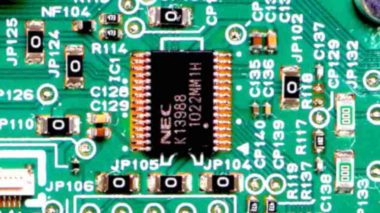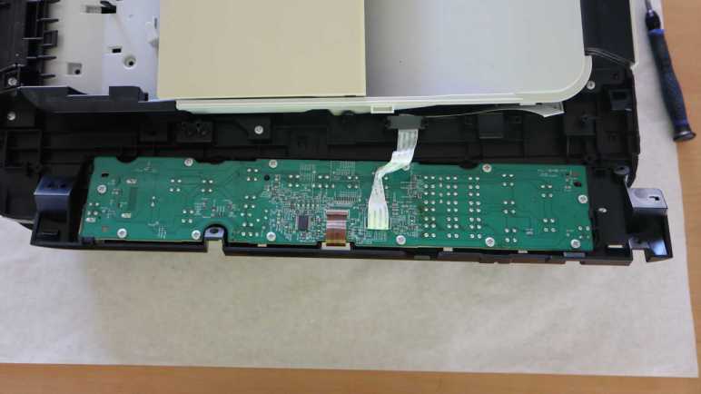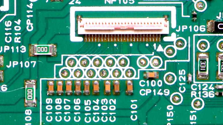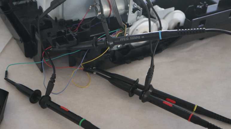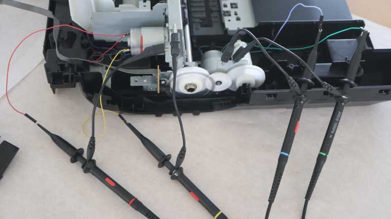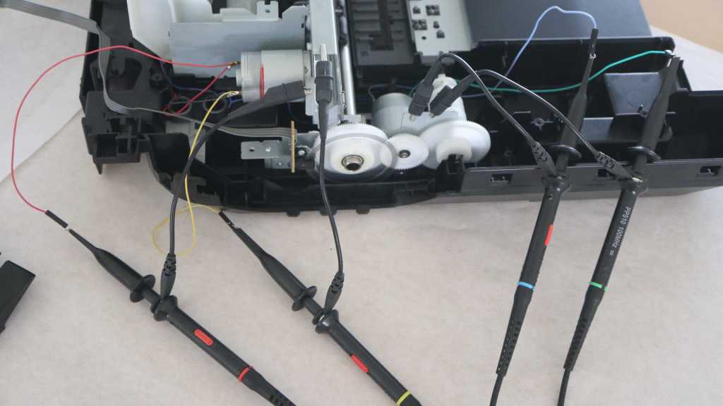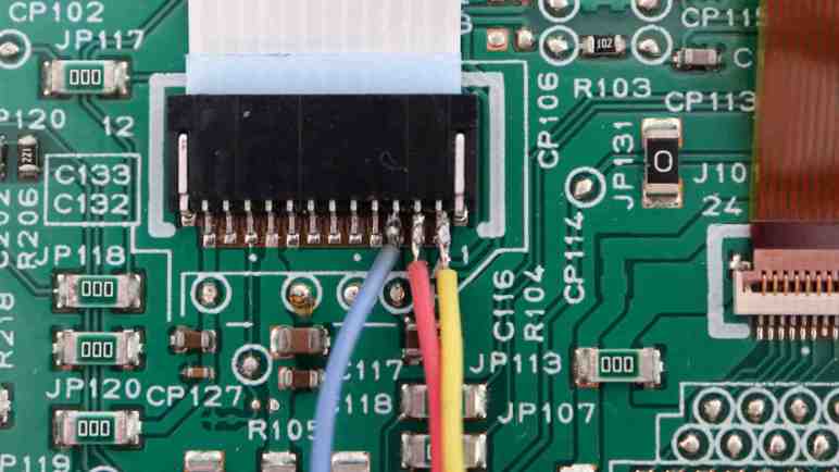
I’ve got the control panel of a Canon Pixma MX340 multi-function inkjet on my workbench, hooked up to my oscilloscope. I’ve located the three wires used for communication between the main board and the control panel circuit board. Monitoring activity of these three wires with my oscilloscope, two of the pins are behaving as communication lines one in each direction and the third has been tentatively identified as a Chip Enable signal for the NEC K13988 chip on board the control panel circuit board.
Before oscilloscope observation, I didn’t know what those three wires were. I thought the best guess was SPI with clock, MOSI, and MISO. I felt I2C was less likely due to its official design intent of communication on the same circuit board, it’s not as robust for running across long ribbon cables. But since I saw no clock signal on any of these three wires, synchronous protocol like SPI and I2C are ruled out. I don’t know any asynchronous protocols aside from old school serial, so I hoped that was it. I went back to my first tutorial of asynchronous serial published by Sparkfun for comparison against my set of oscilloscope traces.

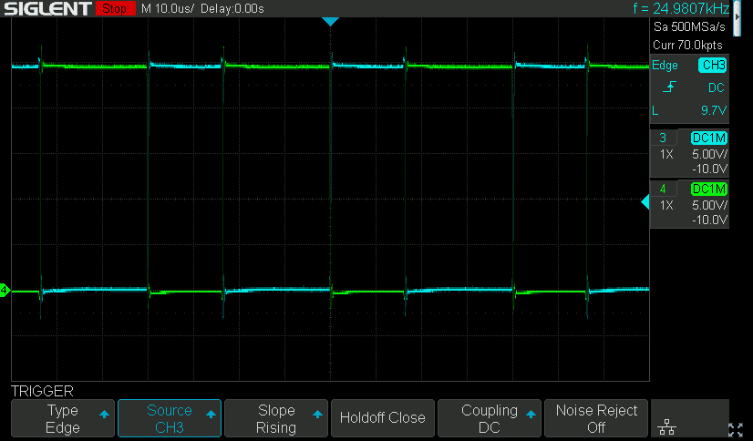
Here was the transmission from control panel to main board, reporting the press of “Back” button. (Leftmost of four buttons under the LCD screen.) Horizontal scale is 5us per grid here, and each state is held for less than one grid. Five of them seem to fit nicely in four grids, so call it 4us per bit. If I interpret this graph as serial data, I would get: 0 for the start bit, 11001001 for 8 data bits, 0 would represent an even parity bit, and a final 1 bit as stop bit. This is consistent with serial. Repeating the exercise with my remaining button press traces, they all had patterns that made sense as 8E1 serial data.
As for the speed, 115200 baud is pretty common for microcontroller projects I’ve examined. 1/115200 = 8.68us, about double the time for each of these bits, implying this is double that speed in the neighborhood 115200 * 2 = 230400 baud. So I will try interpreting this data as 8E1 serial data at 230400 baud and see how far I get.
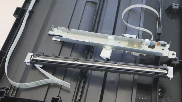
This teardown ran far longer than I originally thought it would. Click here for the starting point.