I’ve successfully made a simple Larson Scanner demo from the faceplate module of a Toyota 86120-08010, the stock tape deck audio head unit of a 1998 Toyota Camry LE. It gave me confidence that I wouldn’t need the original mainboard anymore.
Nor would I expect to want to probe communication between the original mainboard and the faceplate, both separately and alone. Time for a little cleanup work, undo the tangle of wires and get to something more streamlined.
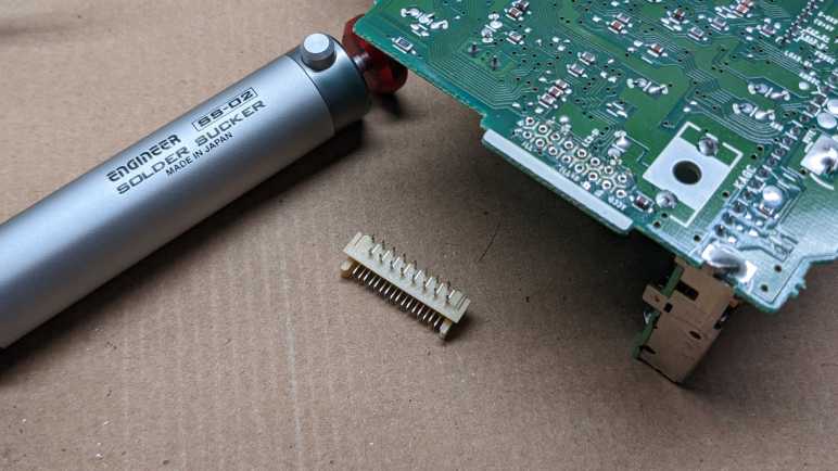
The excellent Engineer SS-02 solder sucker helped me remove all the solder attaching the mainboard connector, freeing it for reuse.
Good news: This connector has two rows of easy-to-solder through-hole pins, with the 0.1″ pitch common to perforated prototype boards. The two rows are 0.1″ apart as well.
Bad news: The two rows are staggered, which won’t fit on a 0.1″ perforated prototype board. Reusing this connector properly will mean a custom circuit board.
In the meantime, I can still make use of that connector even if “improperly”. I had soldered wires directly to the faceplate for probing and experimentation, but I can move all of those wires to that connector even without a circuit board.
Soldering wires directly to the pins isn’t best practice, but it allows me to move and store this assembly with less worry I’ll accidentally yank something off the faceplate.
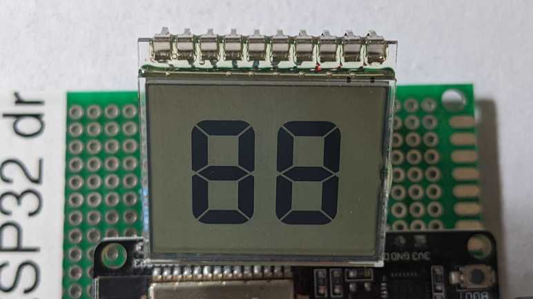
I am happy with a sense of accomplishment after I deciphered all the information necessary to utilize this circuit board, formerly the faceplate for a salvaged car tape deck. I started this investigation when I found I could power it up under control of the original mainboard. Now, I can work with the LCD and read all knobs and buttons with an Arduino, independent of the original mainboard. My original intent was just to see if I could get to this point. I thought I would learn a lot whether I succeeded or failed trying to control this faceplate. I have gained knowledge and experience I didn’t have before, and a faceplate I can control.
Now what?
It feels like I should be able to build something nifty with this faceplate, there’s room to be creative in repurposing it. At the moment I don’t have any ideas that would creatively utilize the display and button/knob input, but I could build a simple demo. This LCD is wide and not very tall, so I thought I would make it into a simple Larson Scanner. (a.k.a. Cylon lights a.k.a. K.I.T.T. lights.)
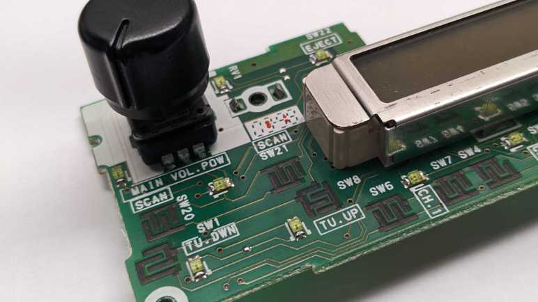
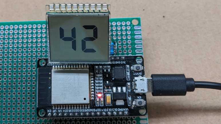
First, I divided the LCD segments into 16 groups of roughly similar size. I started using my segment map to generate the corresponding bit patterns by hand but then decided I should make a software tool to do it instead. I’ve already written code to light up one segment at a time for generating the segment map, it took only a bit of hacking to make it into a drawing tool. I use the knob to move segments as I did before, but now I could press the knob to toggle the selected segment. Every time I pressed the knob, I print the corresponding bit pattern out to serial terminal in a format that I could copy into C source code.
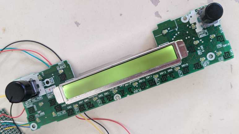
I then added a different operating mode to my Arduino test program. Pressing the Volume knob would toggle between drawing mode and Larson Scanner mode. While in Larson Scanner mode, I would select two of those 16 groups based on scanner position, and bitwise OR them together into my display. This gives me a nice little demo that is completely unrelated to this LCD’s original purpose, and confidence I no longer need this tape deck’s original mainboard.
It is time to wrap up investigation into the workings of a tape deck faceplate, salvaged from the stock audio head unit of a 1998 Toyota Camry LE. I believe I’ve deciphered all the information necessary to reuse this faceplate independently from the rest of the tape deck. Summarized in this pinout report with links to more details.
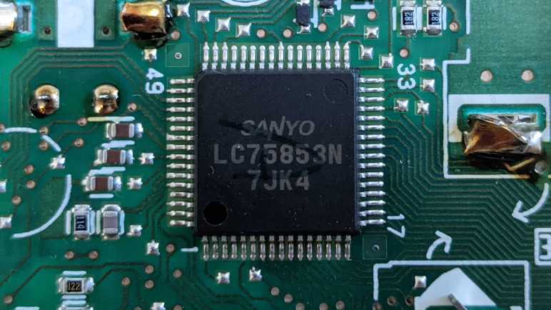
The faceplate circuit board is largely built around a Sanyo LC75853N chip, which communicates via a Sanyo proprietary protocol called CCB (Computer Control Bus). An external microcontroller (I used an Arduino Nano in experiments to date) can dictate what is displayed on the LCD (see segment map here) and scan pressed/not-pressed state of buttons (see button map here).
Some faceplate components are independent of LC75853N:
CCB clock signal. Active-low generated by microcontroller.
LCD-CE
CCB enable. Active-high generated by microcontroller.
CD-EJE
Eject button. Normally open, shorts to GND when “Eject” button is pressed.
ILL
Illumination power supply (positive). +5V to +14.4V (~60mA) relative to ILL- for variable button backlight brightness.
LCD-BL
LCD backlight power supply (positive). +6V (~60mA) relative to BL-
VOL.CON
Volume control potentiometer. Voltage between ACC5V (full clockwise) and GND (full counterclockwise)
PULS-A
Audio mode quadrature encoder knob – A ACC5V or GND, will be opposite of B when at a detent. A and B briefly identical during transition between detents.
PULS-B
Audio mode quadrature encoder knob – B ACC5V or GND, will be opposite of A when at a detent. A and B briefly identical during transition between detents.
GND
Digital logic power (negative). Relative to ACC5V
ILL-
Illumination power supply (negative) Relative to ILL
BL-
LCD backlight power supply (negative) Relative to LCD-BL
RESET
Unknown. Observed 0V relative to GND. LC75853N has no reset pin. Seems OK to leave it unconnected/floating.
Unknown. Observed 0V relative to GND. Seems OK to leave it unconnected/floating.
I’ve mapped out all LCD segments on a Toyota 86120-08010 tape deck faceplate, allowing me to control what is displayed from an Arduino. Constrained by the nature of a segmented LCD, of course. These segments were customized for a tape deck, doing what it needs and no more. Any projects trying to repurpose it would have to get creative. This will be even more difficult than abstract Nyan Cat on a VCR VFD!
But I have more than just the LCD, I have the entire faceplate which gives me option for user interactivity. Two knobs which I still have, and buttons which are now gone but their electrical traces are still present. I can find something conductive to bridge these traces like the buttons used to do, or I can solder wires connecting to switches elsewhere. Either way, I needed to write code for my Arduino to read key scan data from the Sanyo LC75853N chip. Just like LCD segment control data, my goal is to emulate the original mainboard as closely as I can. I will be guided by the datasheet and what my logic analyzer captured.
Thanks to lessons learned from doing LCD segment control CCB communication, reading keyscan data over CCB was relatively straightforward and I could dump control data out to Arduino serial monitor.
I will follow the KD1-KD30 numbering system used in the datasheet timing diagram.
Button map for Toyota 86120-08010 faceplate. (Click to view full size)
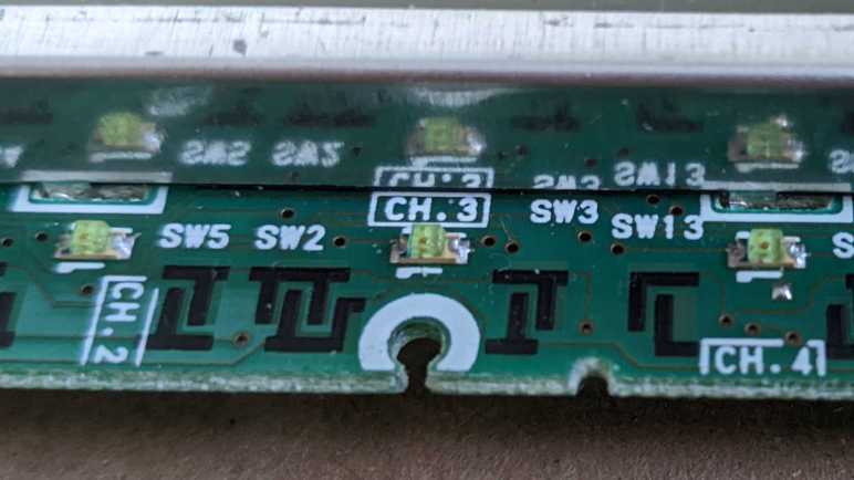
This key map shows the KD number for almost all of the buttons on the faceplate, including the push action on both knobs. The lone exception is the “Eject” button, which has its own dedicated wire and is not part of LC75853N key matrix. These numbers may look odd at first glance, but they make sense once we look at how they would be wired to the LC75853N:
These fifteen buttons make use of KS3-6 and KI2-5, learning only KD14 unused in its matrix. If I wanted to add in a single button, I will try to find KS3 and KI4 traces on the faceplate to wire in KD14. If I want to add more buttons, I might need to solder directly to the unused IC pins KI1, KS1, and KS2 as I wouldn’t expect any traces for those unused pins on the faceplate circuit board.
Feeling good that I’ve figured out the input & output of this faceplate, it’s time to wrap it all up.
Thanks to well-labeled connectors and an online datasheet, I can write Arduino code to control faceplate LCD of the stock tape deck audio unit from a 1998 Toyota Camry LE. (86120-08010). However, knowledge of the digital wiring doesn’t tell me anything about the physical location and shape of each segment in the LCD. I will build a segment map with the help of a knob already on the faceplate. The Sanyo LC75853N chip could control up to 126 segments. I edited my Arduino program to turn on all of them, so I could take this picture to see where segments even existed.
It reflected the custom nature of a segmented LCD. Some of these digits would only ever display numbers, so they had the standard 7 segments for numeric display. Others have a secondary use to display letters for a few audio settings, and those digits had more than 7 segments. But they can’t display arbitrary letters, only exactly what was needed and no more.
With the full set of available segments in hand, I changed the program to turn on just one segment at a time interactively selected via the “Audio Mode” knob. Since each segment is a single bit, I could print out my control bits to Arduino serial monitor to see current active segment’s programmatic address.
I’m using the same numbering system as used in the datasheet, D1 to D126. From there, I generated this segment map:
LCD segment map for 86120-08010. Click to view full size.
When I first started my Arduino program, I saw nothing for the first few turns of the dial. I thought perhaps my program was faulty, but a few turns later I saw my first result for D13. From there on it was relatively straightforward, working from bottom-to-top and right-to-left. Some notes:
D24 is missing, a mysterious gap.
There were a few segments that I had thought were separate but were actually the same segment. For example, two visually distinct segments were actually just D54. This was disappointing, because it restricted the number of letters we could show. (Example: a good looking “M” would be possible, but a good looking “N” wouldn’t.)
Along the same lines, some numeric segments looked like separate segments purely for the sake of preserving the 7-segment aesthetic. The three segments D101, D102, and D105 together could display either “1” or “2” but visually looked like 6 segments instead of 3.
The leftmost large numeric digit puzzled me. It could only display 1, which is fine. But given that, why are the two segments D91 and D92 individually addressable? I can’t think of a reason why we’d want to display only the top or bottom half of a “1”.
Here is a table from the LC75853N datasheet mapping segment numbers to pins. I colored in the segments that were seen and a clear pattern emerged: This LCD allocation avoided using the first four pins (S1-S4) leaving the option of using them as general-purpose output wires. (P1-P4) At the end, stopping at D105 meant they didn’t have to wire up the final seven output pins. (The final two S41 and S42 would have had to been reallocated from key scan duty KS1 and KS2, if used.)
None of this explains why D24 is missing. The answer to this mystery must lie elsewhere.
Now that I know what is on this LCD available to display, maybe I can think of a creative way to reuse it. While I think that over, I’ll proceed to work through how to read input from this faceplate.
Once I got a retired faceplate’s LCD up and running, I realized I was wrong about its backlight circuitry. Now that it’s been sorted out, attention returns to the LCD. I want to map out all the segments, which means I need to get some way to interactive select individual segments. Recently I’ve used ESPHome’s network capabilities for interactivity, but this project uses an Arduino Nano for its 5V operating voltage. I can wire up my own physical control, but the faceplate already had some on board. Earlier probing established Power/Volume knob is a potentiometer, and Audio Mode knob is a quadrature encoder with detent.
The encoder is perfect for selecting individual segments. I can write code to activate one segment at a time. When the knob is turned one way, I can move to adjacent segments in one direction. When the knob is turned the other way, segment selection can follow suit. However, this knob does have one twist relative to my prior experience: Each detent on this encoder is actually two steps. When the knob is at rest (at a detent) the A and B pins are always different. (High/low or low/high). Intermediate values where A and B pins are the same (high/high or low/low) occur between detents.
This places timing demands for reading that knob. For encoders where each detent is a single step change and turned by human hands, polling once every hundred millisecond or so would be fast enough. However, since this knob can flash through a step very quickly between detents, I need to make sure those steps do not get lost.
There are many quadrature encoder libraries available for the Arduino platform. I selected this one by Paul Stoffregen, who I know as the brains behind the Teensy line of products. When working with interrupt-capable pins, this library will set up hardware monitoring of any changes in encoder state. This makes it very unlikely for encoder steps to get lost. According to Arduino documentation for attachInterrupt(), all ATmega328-based Arduino boards (including the Arduino Nano I’m using) have two interrupt-capable pins: 2 and 3. Using those pins resulted in reliable reading of knob position for mapping out segments of this LCD.
I’ve successfully programmed an Arduino to interface with LCD controller on the faceplate of a retired car tape deck. When under the control of its original mainboard, the LCD segments and the LCD backlight always turned on and off in lockstep, leading me to think LCD backlight was under control of the LCD segment controller. But now that I have active LCD segments but no LCD backlight, I know my assumption was wrong. I’ll need to look elsewhere.
Looking at my notes from measuring voltage of each pin relative to data ground, two candidates stood out because their voltage levels changed when the LCD was active vs. inactive. When the LCD is on, there is ~6V difference between them. And when the LCD is off, there is ~0.5V between them. One candidate’s label was cropped at the bottom. Earlier I guessed maybe it said “CD-BL” but now that I look closer, I think the vertical bar to the left is part of the text: a “L” with its bottom cropped. That label is possibly “LCD-BL” which I optimistically expand to “Liquid Crystal Display Back Light”. The other candidate pin is labeled “BL-” which would be the negative terminal. Notably, “BL-” fluctuated relative to “GND” so these two pins, if they are our targets, have their own voltage planes.
The first test was with my backlight LED tester, which quickly shot up to the preset current limit of 20mA at less than 1V while the backlight stayed dark. I then measured with an Ohm meter, which indicated just 10 Ohms between these two pins. If that is a LED current-limiting resistor, it is the smallest I’ve ever measured. Might this backlight be some technology other than LEDs? I don’t know how a compact fluorescent light would look like under an Ohm meter. (I do know a filament bulb usually shows up as a short a.k.a. direct connection with no resistance.) I can’t see the actual light source, as it is buried within the metal case of the LCD assembly.
Well, this is a piece of salvaged electronics and I have little to lose. Especially since I believe the backlight is on its own circuit. So if I accidently destroy the backlight, I still have the rest of the faceplate to play with. I soldered wires to “LCD-BL” and “BL-” and connected it to my bench power supply. Gradually turning up the voltage, I start seeing a dull glow at just under 5V and got brighter as it reached 6V.
Illumination of this backlight isn’t great, but consistent with how it looked when I powered it up with the original mainboard.
The diffuser behind this LCD isn’t nearly as good as what we see behind, say, the screen of an Amazon Fire tablet. But it works well enough for us to see the LCD segments in the dark, and that’s all it needed to do in a car. These LEDs do not need to be daylight visible, as the LCD is readable in the presence of ambient daylight without backlight help.
At 6V this backlight drew almost 70mA, which is LED territory after all. If this was a piece of cheap consumer electronics, I would say 70mA indicates three heavily-driven LEDs. But this is from a Toyota, a brand with reputation for engineering for longevity. So I’m going to assume it actually represents four (or more) lightly driven LEDs. I increased the voltage until 9V, at which point it drew 80mA and was still pretty dim and uneven. I guess “bright enough to be legible at 6V” is all we’re going to get out of this backlight.
Since I had the bench power supply set up for testing LEDs anyway, I connected wires to two other pins “ILL” and “ILL-” which I had already determined to be on their own independent voltage plane as well. These wires are connected to the in-car dashboard illumination circuit, which has a dimmer knob. Being on a separate power plane explains the behavior I remember from using this tape deck in the car: lights illuminating faceplate buttons would change in brightness as I moved the dimmer knob, but the LCD backlight LED stayed at constant illumination. When I powered them directly on ILL/ILL-, I start seeing a tiny bit of glow at just over 5V (<10mA) and brighter as the voltage is increased.
I stopped at 14.4V (80mA) which is the maximum recommended voltage level for automotive lead-acid batteries, and thus likely to be the ceiling for automotive electrical systems like this one.
Between these two sets of lights, it means any project to repurpose them will need to generate multiple voltages. Up to 14.4V for button backlights (variable if we want dimming), 6V for LCD backlight, and 5V for digital logic including physical controls like the Audio Mode knob.
Using a Saleae Logic 8 Analyzer, I’ve examined the communication protocol between the mainboard and faceplate of a car tape deck. These signals match expectations of a Sanyo LC75853N LCD controller which uses Sanyo’s proprietary CCB (Computer Control Bus) protocol. CCB has some resemblance to SPI and I2C but is neither, though close enough to SPI for me to use the SPI analyzer mode on a Saleae analyzer.
But “close enough” won’t be good enough for the next step: take an Arduino Nano and write code to talk to the LCD controller via CCB, copying the data waveform behavior I saw as closely as I can. Arduino has a library for SPI that assumes control of the enable pin, which has different behavior under CCB so that would not work here. I investigated using the shiftIn() and shiftOut() routines, which is part of the standard Arduino library. They are software implementations of a clocked serial data transfer routine, but unfortunately their clock signal behavior is different from what I saw of CCB under the logic analyzer. (Active-low vs. active-high.) In order to emulate behavior of the tape deck mainboard, I would have to write my own software implementation of CCB serial data transfer.
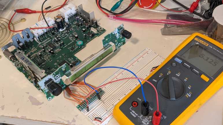
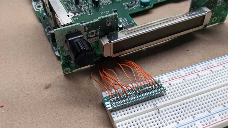
On the hardware side, I could no longer avoid soldering to small surface-mount connector pins on the back of the faceplate. I started simple by soldering the four data communication wires: LCD-DO, LCD-DI, LCD-CLK, and LCD-CE. Probing the circuit board with my meter, the only alternative soldering points were directly to the LC75853N, and those pins are even smaller. However, I found alternatives for ACC5V and GND: those were directly connected to the volume control potentiometer, which has nice big through-hole pins for me to solder to. I soldered these wires to a small prototype board with header pins, which then plugged into a breadboard alongside my Arduino Nano.
As a “Hello World” for CCB, I wrote code to replicate the control signals as closely as I could. I won’t try to replicate the exact timing of every pulse captured by my logic analyzer because (1) Arduino doesn’t make that level of control easy and (2) the CBB spec has no explicit requirement for precise timing anyway. However, I aim to make sure relationship between every clock, data, and enable pin high/low transition is preserved. I can verify this by capturing my Arduino output and compared the output to what I captured from the tape deck mainboard, look for where they are different, and fix differences over several iterations. Finally, I was satisfied the data waveforms look the same (minus the timing caveat above) and connected the faceplate.
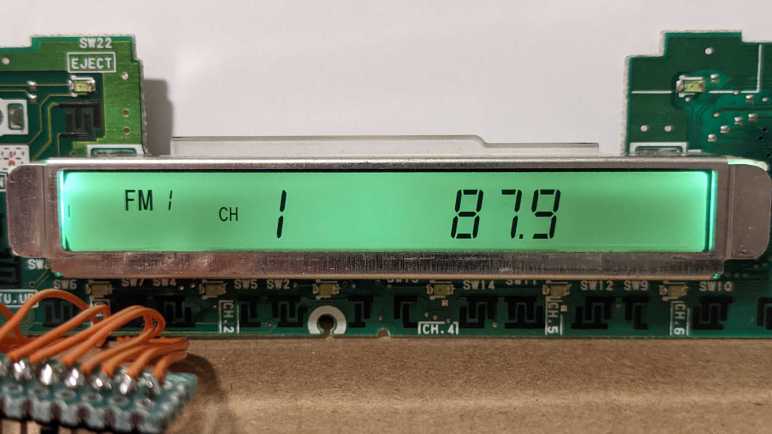
These are almost the same LCD segments that are visible when I captured the data communication between mainboard and faceplate.
The only difference I see is “ST” in the upper right, which lights up when the FM tuner has a good enough signal to obtain stereo audio. Since this tape deck didn’t have an antenna attached, “ST” blinks on and off. Apparently, I had taken this picture when “ST” was on, and the recorded control signal I played back on an Arduino was when it was off. This is close enough to call my first test a success.
The other visible difference was the backlight: illuminated when I captured the data control message, but dark when I played it back. I had hoped the backlight was under LC75853N control somehow, but it looks like those LEDs are actually separately controlled.
I’m learning to understand control communications for a Sanyo LC75853N, which drives the LCD in the stock tape deck head unit of a 1998 Toyota Camry LE. My goal is to control the faceplate independent of the rest of the head unit, which means learning about Sanyo’s proprietary CCB (computer control bus) protocol. CCB resembles some parts of SPI and some parts of I2C but is neither of them. I was primarily focused on the LCD output, but in setting up my logic analyzer to look at LCD output control, I also have everything to examine keypress input.
Here is the Saleae logic analyzer output for the chip reporting that the volume knob was pressed, which is designed as the on/off toggle for this tape deck. The controller toggled LCD-CLK 32 times during this data transmission. Datasheet says the first 30 bits represent state for each of the scanned keys, followed by one bit representing sleep state, and one bit of padding whose state is irrelevant. Here the 0x08 represents the single scanned key that corresponds to the knob being pressed.
Before that happened, though, were several events of note. When a CCB peripheral wants to report data to the controller, it pulls the DO line low. (Spec sheet says DO has a 1k – 10k pull-up resistor.) It then waits for the controller to emit a peripheral address and then raise CE.
If the controller emitted the peripheral’s address, then it can start using DO to report bits upon each CLK pulse.
If the controller emitted another peripheral’s address, then it releases DO (letting it be pulled high again) and wait until CE is low, at which point it pulls DO low again.
When I read this part of the spec, I was confused at how the LC75853N would know whether to transmit or to receive when its address was called. Eventually I found the answer: it has two different addresses! Address 0x42 receives LCD data from the controller, and address 0x43 reports key scan data to the controller. I had missed the difference when I looked at the logic analyzer output earlier, 0x42 looked a lot like 0x43 when I was skimming through output. But it’s plainly there once I was paying attention. Address is transmitted on DI from the least significant bit first: 1100 0010.
Counting buttons on this faceplate, I don’t think it wired up all 30 possible key scans. But aside from the power button (pressing volume knob) logged here, I don’t know what they are. I might map them once I can perform CCB communication to read these key press reports. And if I fail to do that… I guess I wouldn’t care anyway. Onward to the Arduino!
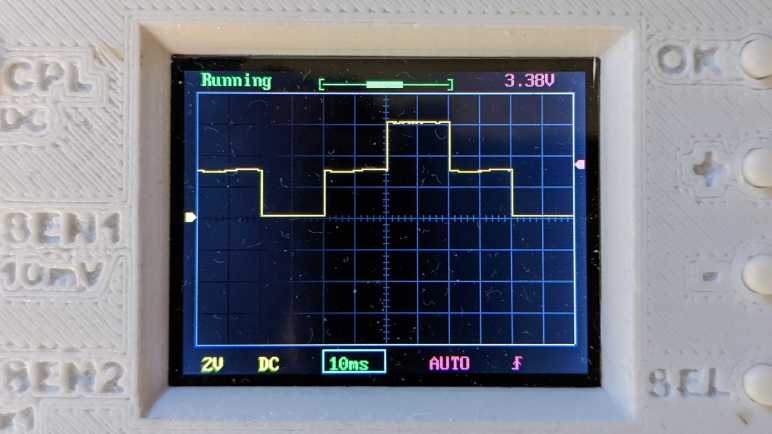
My Saleae Logic 8 analyzer is now tapped into communication between the mainboard and face plate of a tape deck. A quick examination of the captured data looks reasonable, now it is time to dig into the data, compare against the LC75853 datasheet, and understand what is going on with LCD output control.
Within the ~3/4 second of the faceplate getting power, this sequence is transmitted repeatedly approximately once every 5 milliseconds. Zooming in, I see they are three consecutive CCB transmissions to address 0x42:
Address
1
2
3
4
5
6
7
0x42
0x00
0x00
0x00
0x00
0x00
0xC0
0x10
0x42
0x00
0x00
0x00
0x00
0x00
0x00
0x80
0x42
0x00
0x00
0x00
0x00
0x00
0x00
0x40
Guided by the datasheet, I interpret them as:
Most of the 0x00 bits indicate the corresponding LCD segment is to be turned off.
Some of the 0x00 bits in the second and third set are fixed data.
In the first set, the two bits in 0xC0 maps to S0 and S1, which controls sleep mode. S0 =1 and S1=1 is one of three available sleep modes.
Also in the first set, the single bit in 0x10 translates to SC, the segment on/off control data. SC=1 means display state is off.
For the second and third set, they each have a single bit that appear to be fixed within the section labeled as DD (direction data) and their values written into the timing diagram.
After that initial ~3/4 of a second, the pattern makes a minor change and repeats less frequently: once every 50 milliseconds:
Address
1
2
3
4
5
6
7
0x42
0x00
0x00
0x00
0x00
0x00
0x00
0x10
0x42
0x00
0x00
0x00
0x00
0x00
0x00
0x80
0x42
0x00
0x00
0x00
0x00
0x00
0x00
0x40
The two bits associated with sleep mode are now zeroes. Sleep flags S0=0 and S1=0 means “Normal operation”, so the chip is awake. SC is still 1, though, so LCD is still off.
Then I pressed the power button. This triggered a set of events (probably related to key scan reporting) that I will investigate later. Right now, I am focused on how the LCD control message changed to display “FM 1 CH 1 87.9”
Address
1
2
3
4
5
6
7
0x42
0x00
0x00
0x00
0xD0
0xDD
0x02
0x00
0x42
0x70
0x55
0x00
0x00
0x00
0x00
0x80
0x42
0x06
0x04
0x0B
0x00
0x00
0x00
0x40
The end of first set changed from 0x10 to 0x00. This cleared the SC flag, so now LCD is on. There are other control bits in the first set of bytes and they are all zero.
K0 and K1 set to zero means none of the key scan pins were reassigned to segment control duty, so the chip retains ability to scan up to 30 keys.
P0 and P1 set to zero means none of the segment pins were reassigned to digital output duty, so the chip can control a maximum of 120 segments.
DR set to zero means 1/3 bias drive voltage.
The display backlight is also illuminated now, but which of these bits are responsible? For now, that is still an unknown. Until I get more information otherwise, I’ll proceed on the assumption that all remaining bits are LCD segment control.
To get more information, I pressed the “Mode” knob changing the display to “BAS 0” and its control message to this:
Address
1
2
3
4
5
6
7
0x42
0x00
0x00
0x00
0x00
0xC0
0x02
0x00
0x42
0x0D
0x80
0xDC
0xF4
0x2F
0x02
0x80
0x42
0x00
0x00
0x00
0x00
0x00
0x00
0x40
That’s a lot of changes!
For a smaller delta, I turned the knob one step so it now shows “BAS 1”.
Address
1
2
3
4
5
6
7
0x42
0x00
0x00
0x00
0x00
0x80
0x02
0x00
0x42
0x00
0x80
0xDC
0xF4
0x2F
0x02
0x80
0x42
0x00
0x00
0x00
0x00
0x00
0x00
0x40
This is a more manageable set of changes. A single step changes “0” to “1”, which on a 7-segment display means turning off four segments. A change from 0xC0 to 0x80 turns off one bit, and from 0x0D to 0x00 turns off three bits. This matches expectation of deactivating four segments.
I didn’t take pictures for the next experiment: While in FM radio mode, I press the tuner up button once. This moved it off the first preset so “CH 1” disappeared and now the display shows “FM 1 88.1”:
Address
1
2
3
4
5
6
7
0x42
0x00
0x00
0x00
0x10
0xD1
0x02
0x00
0x42
0x7F
0x55
0x00
0x00
0x00
0x00
0x80
0x42
0x00
0x00
0x0B
0x00
0x00
0x00
0x40
Then I pressed it again, so it now displays “FM 1 88.3”:
Address
1
2
3
4
5
6
7
0x42
0x00
0x00
0x00
0xD0
0xD9
0x02
0x00
0x42
0x7F
0x55
0x00
0x00
0x00
0x00
0x80
0x42
0x00
0x00
0x0B
0x00
0x00
0x00
0x40
All changes are in the first part of the control message. Changing from 0x10 to 0xD0 turns on two bits, 0xD1 to 0xD9 turns on one bit. These added up to the three activated segments, matching expectation of going from a “1” to “3” on a seven-segment numeric display.
These observations give me confidence that we are indeed looking at control bits corresponding to individual segments on screen. Not enough information to map out all the segments to their corresponding bits, but I am postponing that task until I have individual control through code. It would be much easier to map out segments when they are under my control. And if I fail to obtain control, I wouldn’t care about the segment map anyway.
I’m examining the control signals for a Sanyo LC75853N LCD driver chip, which uses a Sanyo proprietary protocol they call CCB. (Computer Control Bus.) It’s popular enough that I could find CCB reference material online, but it’s not popular enough to be natively understood by Saleae’s Logic Analyzer software. Beyond Saleae’s set is a list of Community Shared Analyzers but Sanyo CCB didn’t make the cut there, either. Those additional analyzers were written using Saleae’s Protocol Analyzer SDK so there is the option to write one for CCB. For the purpose of initial experimentation, though, their default SPI analyzer is close enough.
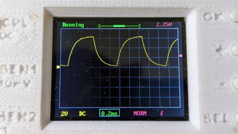
Before we even try using the SPI analyzer, we can look at the raw data. CCB transmits the peripheral address before raising CE. Here I can see 0x42 hexadecimal, or 0b01000010 binary. (The white binary numbers were not part of Saleae software, I drew it in afterwards.) In an unfortunate bit of coincidence, this binary value is symmetric so it alone couldn’t tell us if CCB transfer least-significant bit first or most-significant-bit first. According to spec, it is least-significant-bit first. Seeing this gave me the confidence I’ve wired up everything correctly for further probing.
The clock pulses measured out to be in the ballpark of 400kHz, which I can probably work with. But more importantly, I was relieved to see that the clock pulse widths varied somewhat between transmitted bits. This is encouraging because it meant the protocol is graceful under irregular clock pulses, making it more likely I can successfully communicate using CCB in software. Which is great because I don’t have dedicated CCB communication peripheral hardware.
The next step was to activate SPI analyzer with the following parameters. The biggest difference between CCB and SPI is the behavior of CE line, and thankfully Saleae’s SPI analyzer can be configured to ignore CE. (“Enable” set to “None”.) I set the SPI analyzer options to the following values to decode all the values regardless of CE status:
SPI Analyzer Option
Value
MOSI
LCD-DI
MISO
LCD-DO
Clock
LCD-CLK
Enable
None
Significant Bit
Least Significant Bit First
Bits per Transfer
8 Bits per Transfer
Clock State
Clock is High when inactive
Clock Phase
Data is Valid on Clock Trailing Edge
Enable Line
(Doesn’t matter when “Enable” is “None”)
Now the software can decode data for us. This time, the decoded values 0x42, etc. in this image was drawn by the software.
This was the start of the very first data transmission after I applied power to the tape deck. Which is why CLK started as low even though it is normally high when inactivity. When Enable is set to None, I see all the data regardless of CE status.
First question to answer: the B in CCB is “Bus”. How many devices are on this bus? Taking advantage of the difference between CCB and SPI, I can tell the SPI analyzer to decode just the CCB address by saying CE is Active Low:
SPI Analyzer Option
Value
Enable
LCD-CE
Enable Line
Enable is Active Low
The decoded values on LCD-DI were all 0x42, which tells me the LCD control chip is the only peripheral on this bus, which makes things simpler. I won’t have to worry about reading data intended for the wrong device. And once I decided I didn’t have to worry about different addresses anymore, I can switch the SPI Analyzer over to Active High CE. This will cause the analyzer to ignore addresses (since I expect them to all be 0x42) transmitted while CE is low and decode just the data.
SPI Analyzer Option
Value
Enable
LCD-CE
Enable Line
Enable is Active High
Within the ~3/4 second of the faceplate getting power, something is transmitted repeatedly approximately once every 5 milliseconds. Zooming in, I see they are three consecutive CCB transmissions to address 0x42:
I’ve soldered wires to the connector between the mainboard and faceplate of the stock tape deck audio head unit from a 1998 Toyota Camry LE. (86120-08010) My goal is to learn enough to control the faceplate with my own creation independent of the mainboard. Since these two circuit boards can still be powered up, I can probe their voltages and listen to communications between them. A skilled electronics hacker can make sense out of the waterfall of bits, but I don’t have that level of skill yet. I need a little more information, and I started with this very prominent chip on the faceplate.
I couldn’t find where Sanyo hosts their electronic component datasheets, I kept stumble into unrelated areas like their consumer electronics site. This is a common problem when dealing with products made by huge companies with diverse product lines. There’s also the problem that Sanyo has been acquired by Panasonic in 2011 (Wikipedia) so it’s quite possible the relevant divisions have been merged or shut down and their website disappeared.
Seeking another source, I searched for this chip at Digi-Key. Their database did not list this exact item, but there were a few other LC7583 variants listed as “Obsolete” and without datasheet. I ultimately resorted to going through one of those internet sites that archive old PDFs. I find it annoying to have to wade through a bunch of “Click here to download!” ads that try to trick you into downloading irrelevant things that may or may not hide malware. It’s always a hunt for the actual link to the PDF we want, which may or may not have been modified maliciously. But eventually I ended up with Sanyo datasheet for “LC75853NE, 75853NW” which is hopefully close enough. The PDF was also slathered with the annoying site’s watermark, but I hope that’s all the annoyances in that file.
Here is the summary and high-level block diagram:
1/3 duty LCD display drivers that can directly drive up to 126 segments and can control up to four general-purpose output ports. These products also incorporate a key scan circuit that accepts input from up to 30 keys
Digging further into the datasheet, I learned of caveats with that summary. It is not possible to have simultaneous control 126 segments, four output pins, and scan 30 keys. In order to get 126 segments, we have to reallocate two key scan pins cutting the number of scannable keys by 10. And in order to use four output ports, we have to reallocate four segment pins cutting the number of addressable segments by 12. I’m sure such flexibility is useful for adapting to different usages, but it also means I will have to figure out the specific configuration used by this faceplate.
The operating voltage range is listed as 4.5V to 6V, so if I am to build a project to control this faceplate I might have an easier time with 5V parts like Arduino ATmega328P or PIC16F18345. Using parts like ESP32 would require voltage level shifters.
When I examined the connector labels, I noticed enable (LCD-CE), clock (LCD-CLK), data input (LCD-DI), and data output (LCD_DO) pins. I optimistically hoped it meant this chip communicated via SPI, but the datasheet said it actually used a Sanyo proprietary protocol called CCB (Computer Control Bus). I found no official Sanyo documentation here, either, but fortunately CCB was used in enough products that some electronics hackers had preserved a copy of CCB documentation. Like this page, where the author reverse engineered a different car audio head unit (Kenwood KDC-MP6090R) that used a different Sanyo CCB controller (LC75808) so they could control it from a STM32.
CCB have similar pinout as SPI, but its electrical behavior is different. Each device has a hard-coded address similar to I2C. There is a variation of CCB that merges DI and DO into a single half-duplex line, making it even closer to I2C but not still the same. I’m pretty certain I couldn’t use hardware SPI or I2C peripherals to talk to this chip, but in the CCB specification there’s a line “Using software or serial I/O facilities” which implied the creators explicitly supported doing CCB in software. (bit-banging) Looks like some people have claimed success doing so in Arduino so their precedents might be worth a look when I aim to do the same. But before I do that, I need to learn what normal CCB communication looks like.
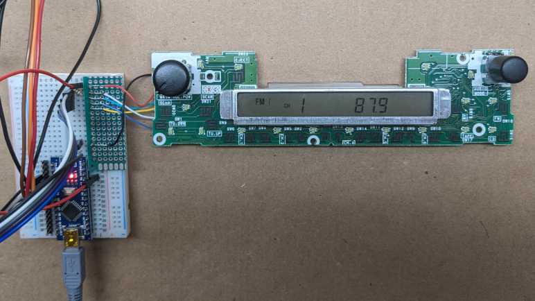
I have on hand electronic circuit boards of the factory stock tape deck unit 86120-08010 from a 1998 Toyota Camry LE. There is a connector between the main board and the faceplate, and I’ve soldered a row of wires so I can take a peek into its inner workings. I thought it might be fun to reuse the faceplate for my own project, creating something that could stand in for the main board.
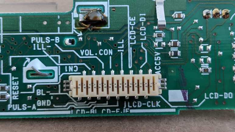
Thankfully, the faceplate side connector was mostly labeled, including the ground pin which gave me a reference point for measuring all the other wires with a voltmeter. Here’s what I found:
[UPDATE: This was my first draft, see the wrap-up post for final draft.]
Perfboard
Connector
Voltage
A
ACC5V
Steady 5V
B
LCD-DO
Steady 5V
C
LCD-DI
Fluctuates
D
LCD-CLK
Fluctuates
E
LCD-CE
Fluctuates
F
(CD-EJE?)
5V
G
ILL
0V when mainboard ILL is 0V (lights off) 12V when mainboard ILL is 12V (lights on)
Quadrature encoder for settings knob. 5.1V – 0.1V – 5.1V as knob is turned.
K
PULS-B
Quadrature encoder for settings knob. 0.1V – 5.1V – 0.1V as knob is turned.
L
GND
0V reference
M
ILL-
0V when lights off 0.7V when lights on
N
BL-
0.7V when radio on 7.5V when radio off
O
RESET
0V
P
?
0V
Notes:
One connector, which I wired to breadboard column P, has no label. It doesn’t seem to do much, either. Possibly unused?
The bottom ~1/3 of two labels were cropped off this silkscreen design. The one I wired to perfboard F might be “CD-EJE”, and H might be “CD-BL”. But it may as well be “CD-BI” or similar letters with the same top 2/3.
I was surprised that LCD-DO appears to hold steady at 5V, I expected it to fluctuate during data transfers. [UPDATE: This is expected for Sanyo CCB protocol in absence of event notification.]
LCD-DI, LCD-CLK, and LCD-CE fluctuates as expected.
There are two knobs on this control panel. They can be both turned and pressed. Turning the volume knob affects VOL.CON, but the press (radio power on/off) seems absent from this connector.
Similar story with the settings knob. Turning it affects PULS-A and PULS-B but pressing (select) is absent from the connector.
I know there is an LCD controller chip on this faceplate circuit board with additional feature to scan for button presses. Perhaps in addition to faceplate buttons it is responsible for reading presses on volume and settings knob? [UPDATE: Hypothesis confirmed.]
If the LCD controller chip lacks ADC (analog-to-digital conversion) and quadrature decoding, that would explain why the connector has VOL.CON, PULS-A, and PULS-B so something on the mainboard can interpret knob motion.
Several LEDs scattered throughout the faceplate turn on when ILL is high. Varying ILL between 9V and 12V controls brightness of these LEDs.
ILL does not control LCD backlight LEDs, whose brightness remains constant. Might the LCD control chip responsible for the backlight as well?
ILL- is a voltage plane that can be 0.7V higher than the GND plane. Have to keep this in mind when wiring up components, in case a 0.7V difference is problematic. Or ILL and ILL- could be wired separately from digital logic aspect of the circuit.
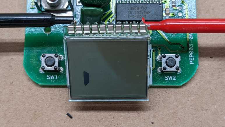
Successfully mapping out the segments for a food thermometer LCD had a nice side effect of improving my soldering skills. Armed with this experience, I feel more confident tackling the task of deciphering LCD controller communication protocol. Earlier I had successfully reassembled and powered up the circuit boards from a 1998 Toyota Camry LE stock tape deck. Now I intend to go beyond looking at pretty lights and see if I can control its front panel.
That front panel connects to the main board through this connector, which has labelled most of its contact points. Since I want to probe their behavior in a running system, I wanted to preserve the ability to plug it back into the mainboard. I had the soldering iron all warmed up ready to solder to the visible surface-mount contacts above and below this connector, but then I thought of a better idea.
Its mating connector is soldered to the mainboard, and it is a through-hole connector which meant there are exposed pins on the bottom of the mainboard. These pins are finer pitch than the 0.1″ I usually work with, but through-hole pins are still more familiar to me than surface mount pads. So I soldered my wires to these pins.
These wires are then brought out to another strip of perforated prototype circuit board, and a row of 0.1″ pitch headers.
Which then plug nicely into a breadboard for easy probing and experimentation. Thanks to the labeled connector, I already know which wire is ground so I connected a bare loop for my instruments to use as reference. Next step is to probe the remaining pins to determine their voltage range.
After figuring out the segmented LCD module salvaged from an electric blanket controller, I revisited the food thermometer LCD that foiled my first attempt at deciphering its multiplex encoding. This time I have a smaller solder tip to maneuver in limited space. I also have finer wires with softer insulation to reduce stress on these solder joints. And finally, instead of individual pins I will solder all of these wires to a perforated prototype board with pin headers, so that they all share physical stress together. The perforated board also had letters across the top, so I had convenient labels for each of the wires: A through W.
These changes solved the wiring continuity problem, but I hadn’t addressed the problem of applying pressure on the elastomeric “zebra strip” to keep it in contact with copper pads on the circuit board. Or at least, not elegantly.
“Not elegantly” meant there are two different types of tape involved, numerous spacers in various locations, and a small clamp all working together to keep that elastomeric strip in contact with the circuit board. If I am to reuse this LCD, I definitely need a better solution than this jury-rigged setup.
But it was good enough for me to obtain this mapping, scribbling things down as I went. In my earlier effort, I decided this screen didn’t use a typical segment/common pin split. I was wrong! Misled by poor electrical connections. This screen used 18 segments that ended up on my perforated prototype board as A through R. The five common pins ended up on S through W.
Once the segment and common pins were identified, I could wire up my test circuit to activate all segments on this LCD. And from this picture, I can translate my scribbled notes into a more legible segment map.
Some notes on this imperfect segment map:
There was crosstalk between pins C and D on my test setup, so they both activate if either is powered. Usually, one is blurrier than the other, but sometimes they look roughly equal and I had to guess which was which. So some of the C/D segments on this map may be reversed. (For example, C3 might actually be D3, and vice versa.)
I had intermittent connection on pin N. N0, specifically, was not seen (It was missing from the hand drawn map above) and was filled in, inferred, via a process of elimination.
The hundreds digit for the two temperatures can only show 1, 2, or 3. The three horizontal elements are all a single segment, and it is missing the segment to show 4. This makes sense for a food thermometer: while an oven can be set to be 400 degrees or higher, our food would be a charred hulk by the time it reaches that temperature so it’s not really relevant for a food thermometer.
The units for temperatures can be “C” or “F” and they only differ by one segment. All the remaining segments are fixed together along with a text label and the degree symbol. (B3 and Q3.)
R behaved strangely. It is associated with the “Timer” text in the upper right and the middle horizontal segment of “F” in the lower right. They seem to both illuminate regardless of which common pin is active, but that doesn’t make sense because there’s no reason for “Timer” text to be mutually exclusive with using Celsius units. Additional investigation is needed here but that requires individual segment control that I currently lack.
If I want to play with this LCD further, the first requirement is to get a better mounting system to send signal through that elastomeric strip. No tapes, spacers, or clamps. And in order to have individual control over segments, I’ll need either a dedicated LCD driver chip or a microcontroller with at least 18+5 = 23 GPIO pins. This is far beyond the number of pins available on an ESP32 so I’ll need to get up to speed on some other microcontroller if I want to tackle such a project.
For now, this LCD will not go back to the “I don’t know if I can use it” pile of salvaged electronics. It has been upgraded to the “I know I can use it and I’m waiting for a project idea” collection. I love making such an upgrade, and I want to see if I can do the same for a salvaged automotive tape deck faceplate.
I now have imperfect but working control of a 2-digit 7-segment LCD module salvaged from a Sunbeam PAC-215 electric blanket controller. I used an ESP32 for this initial run because I thought I needed voltage control over all ten pins. After a little bit of experimentation, I’ve found that I could probably get away with using 0V and 3.3V directly on each of the segment pins. For the common pins I need an additional option of the midway point 1.65V, but if it is true that an LCD uses very little current, perhaps I could supply that voltage with merely a voltage divider built from resistors? If true, I might be able to control this with something far simpler and less powerful than an ESP32. Perhaps an ATmega328 (Arduino)? Or a PIC16F18345, which has a DAC peripheral and already on hand. (If I’m going to buy a chip, I’ll take Joey Castillo’s suggestion and buy one with LCD control peripheral built in.) These are potential experiments for the future. For now, I want to wrap up work with this particular pair of salvaged LCDs which means leaving good notes for my future self.
I scribbled down this diagram when probing the pins. The pins were numbered before I knew what they did. Now that I know which are segment and which are common, I could label them differently.
I also moved to a zero-based counting system thinking it might be easier to match up to code. Color-coding the different common pins is an idea I picked up from Joey Castillo’s slides, but I wonder if that’s the best way to go. I can’t claim to be an expert on how to use color in a way that’s still accessible to the color blind, and coding common pin information in color risks losing data for scenarios like printing on a black-and-white laser printer.
Moving to letters for segments and numbers for common allows me to put them together as labels on each segment while reducing ambiguity. This is also friendlier to black-and-white printing, but it loses the visual delineation of color coding. Is this better? I don’t know as I see strengths in each. I couldn’t make up my mind on which to keep so I’ll keep both of these diagrams here as references for later.
With this successful milestone of working with LCD modules, I revisited a module that frustrated me earlier.
Once I have some confidence that I can write ESP-IDF code to control voltage levels at a speed relevant for driving a LCD, it was time to move beyond a simple breadboard test circuit. Onward to a perforated prototype board for all ten pins of a simple 2-digit 7-segment LCD, salvaged from an electric blanket controller. In the interest of keeping the wiring simple, I chose ten GPIO pins on one side of this ESP32 dev module I’m using (*) so I could wire everything (almost) parallel.
A 1kΩ resistor connects each ESP32 GPIO pin to an LCD pin, and a 330pF capacitor connects each ESP32 GPIO pin to ground. It isn’t quite a straight shot of ten parallel pins, with a two-wide gap on the left (serial communication TX/RX pins) and a single pin gap on the right (GPIO2, which this dev board connected to a blue LED that I’m using as a system heartbeat indicator.) On the far right is a loop of wire connected to the ground plane, so I have a convenient place for my oscilloscope to clip onto.
That completes the hardware side for my initial test. Moving on to my ESP-IDF project, I started hard-coding a sequence of LEDC PWM duty cycle adjustments that would drive this LCD in a fashion that I believe is called 1/2 duty, 1/2 bias. I think 1/2 duty means switching off between two common segments so each set of segments has 1/2 of the time, and 1/2 bias means the inactive common pin is held at 1/2 of the voltage difference of the active pins. I’m still a beginner so that might be wrong!
I chose to hard code the test because it avoids all the lookup table code I’d have to do if this were to become an interactive changeable display. I have two number digits to work with, so my test pattern is a Hitchhiker’s Guide reference.
The result is clearly legible at the optimal viewing angle, but it fades off quite a bit as the perspective changes. I remember a much wider range of legible viewing angles in its original use, I assume it means I’m doing something different from real LCD driver circuits in this little hack. Possibly related is the observation that, if I illuminate this screen from behind with a LED, its light washes out the LCD.
The original device used two LEDs behind the LCD for backlight, and it didn’t make the digits hard to read, so there’s definitely something missing in my amateur hour LCD controller. But the fact remains it is under ESP32 control, and I learned a lot on my way here. This was the first tangible result of a lot of fumbling around after listening to Joey Castillo’s Remoticon talk on hacking LCDs. Seeing “42” show up on screen is a good milestone to stop and review what I’ve learned.
I used ESPHome and Home Assistant to quickly experiment with parameters for ESP32 chip’s LEDC peripheral for generating PWM (pulse-width modulated) signals, seeing how they looked under a cheap oscilloscope. But for actually driving a segmented LCD, I will need even better control over signal behavior. It is an issue of timing: I need to toggle between high and low states for each common segment pin to generate an alternating signal, and I have two common segments to cycle through. In order to avoid flickering the LCD, this cycle needs to occur at least several tens of times a second.
The tightest control over timing I could get with ESPHome appears to be the on_loop automation, which is generally triggered roughly every 16 milliseconds. This translates to roughly 62Hz which, if I could complete the entire cycle, would be sufficient. But performing all of those toggles within a single on_loop would be too fast for our eyes to see, so we can only take one step in the cycle per on_loop. In order to toggle both high and low on consecutive on_loop, that cuts me down to 31Hz. Then there are two common segments, which cuts it further to 15Hz. I need something faster.
Until I have other tools in my toolbox, the “something faster” I have on hand require going to Espressif’s ESP-IDF SDK. PlatformIO makes ESP-IDF easier to work with, and I’ve had experience with this arena. My starting point (chosen because I’ve done similar things before) is to write a FreeRTOS task dedicated to toggling voltage levels by changing PWM parameters. In between steps of the cycle, I use a FreeRTOS wait (vTaskDelay) to send this task into the background until the next step. This mechanism allows finer control over timing than the ~16ms of on_loop, though it is only slightly better at 10ms by default. Repeating the math above, that works out to 25Hz which would at least be as good as 24fps film. But that is not the limit. Once I’m working within ESP-IDF, I have the option to get even finer timing control. I can get a little bit faster by reconfiguring FreeRTOS tick rate via ESP-IDF’s menuconfig tool. And for ultimate timing control I can start working with hardware timers.
I whipped up a test program to generate a staircase pattern. From 0% duty cycle, to 50% duty cycle, to 100%, then 50%, and repeat with 0%. Running at 20ms per step in the cycle, the timing looks solid. I can easily move this to 10ms and still have a solid square wave.
The 50% PWM value looked almost good enough without a capacitor. (Left) I have a huge pile of 300pF capacitors on hand, so I tried one and the waveform looked much better. (Right.) This is good enough for me to move forward with wiring this signal into a segmented LCD.
I’ve mapped out the segments of a small LCD salvaged from an electric blanket controller. I activated these segments with an ESP8266 that alternated between 0V and 3.3V on two GPIO pins. Good for individual segments, but not good enough to drive the whole display. There are eight segment pins and two common pins for 8*2=16 total possible combinations (14 of which are used for the two 7-segment digits) controlled from ten total pins.
Technically speaking, an ESP8266 has enough GPIO pins, but we’d start intruding into the realm of sharing pins between multiple tasks which is more complexity than I wanted to tackle for a quick test. When driving a LCD, we also want to control voltage levels on these pins and ESP8266 lacks hardware PWM peripheral. For these reasons I will use an ESP32. It has more than enough pins, and hardware PWM peripherals to support generating a voltage on all those pins. ESP32 LEDC PWM peripheral is very flexible, and I need to determine how I want to configure that peripheral.
I used ESPHome because it is a great platform for quick experiments like this. I don’t strictly need WiFi here, but easy integration to Home Assistant and ability to update code over the network are great conveniences. Before I found ESPHome, I would wire up a few potentiometers to the circuit board and write code to use ADC to read their positions. A bit of code will then allow me to interactively play with parameters and see their results. But now, with ESPHome in my toolbox, I don’t need to solder potentiometers or write code for ADC. I can get such interactivity from the Home Assistant dashboard.
By default, ESPHome configures LEDC PWM peripheral to run at a frequency of 1kHz. According to Espressif documentation, it can be configured to run as high as 40MHz, though at that point it really isn’t a “PWM” signal anymore with only a fixed 50% duty cycle. Slowing down the frequency increases the number of bits available for duty cycle specification, and I wanted to find a tradeoff that I think will work well for this project. Here is an excerpt of ESPHome configuration YAML I used for this test.
This allows me to adjust two variables, each exposed to Home Assistant as a monochromatic dimmable light. Which I can change via a slider on a web page instead of a potentiometer soldered to the board. (The gamma correction value was set to 1.0 because we’re not actually controlling a visible light that requires gamma correction.)
pwm_23 controls the PWM duty cycle.
pwm_freq controls the PWM frequency via ESPHome Template Lambda. Theoretically from 1kHz to 10MHz, though in practice we won’t reach either end as the state never gets all the way down to 0.0 nor all the way up to 1.0.
As I adjusted the frequency, ESPHome automatically calculates the duty cycle bit depth.
[15:32:00][D][ledc.output:041]: Calculating resolution bit-depth for frequency 2491148.000000
[15:32:00][D][ledc.output:046]: Resolution calculated as 5
[15:32:00][D][ledc.output:041]: Calculating resolution bit-depth for frequency 2494322.000000
[15:32:00][D][ledc.output:046]: Resolution calculated as 5
[15:32:00][D][ledc.output:041]: Calculating resolution bit-depth for frequency 2497869.000000
[15:32:00][D][ledc.output:046]: Resolution calculated as 5
[15:32:00][D][ledc.output:041]: Calculating resolution bit-depth for frequency 2501411.000000
[15:32:00][D][ledc.output:046]: Resolution calculated as 4
[15:32:00][D][ledc.output:041]: Calculating resolution bit-depth for frequency 2503623.000000
[15:32:00][D][ledc.output:046]: Resolution calculated as 4
[15:32:00][D][ledc.output:041]: Calculating resolution bit-depth for frequency 2505428.000000
[15:32:00][D][ledc.output:046]: Resolution calculated as 4
From this snippet, we can see that 2.5MHz is the limit for 5 bits of resolution. 25 = 32 levels, which gives me control of resulting voltage in (3.3V / 32) ~= 0.1V increments. I think that’ll be good enough.
Here are some plots in oscilloscope form: First the starting point of 50% duty cycle at default 1kHz frequency, before and after adding a 100nF capacitor into the mix.
Not nearly good enough to output 1.65V. To make this better, I can increase the capacitance or increase frequency. Increasing capacitance will dull system response (and I need pretty quick response to rapidly cycle between LCD common pins) so I start cranking up the frequency.
At hundreds of kilohertz without capacitor, the resulting wave is more than what this little oscilloscope can capture at this timescale. When the 100nF capacitor is added in, we see a pretty respectable 1.65V signal, might even be good enough. But there’s plenty of room left to go faster.
Getting into the megahertz range, there’s enough natural capacitance in the system (wires, breadboard, etc.) that we see a pretty good waveform even without a real capacitor in line with the output. But with just a 330pF capacitor (much smaller than the 100nF I started with) the resulting voltage looks pretty good. At least, at this time scale. Now I need to move beyond ESPHome for better control of 2.5MHz PWM signals.
I was so eager I performed a quick LCD test before I even completed the teardown. I got a single segment to show up, which was a promising start. I was also happy to see this LCD connected to its circuit board with nice long metal pins that I could unsolder, not the elastomeric “zebra strip” used by the food thermometer. These pins are even spaced in a breadboard-friendly 0.1″ pitch, win!
I recently got the Engineer solder sucker from Adafruit, upon Helen Leigh’s recommendation and it made this de-soldering task much easier than with my previous lowest-bidder solder sucker. I now recommend the Engineer unit too, it is well worth the price premium.
I tried to put this module directly into a breadboard, but the pins are too fragile. (They would bend instead of pushing into the breadboard.) Thanks to the 0.1″ spacing, it was very easy to solder robust headers onto those pins.
The headers gave me a solid reliable connection to those pins, making it easy to map out all the segments. Far easier than the food thermometer LCD and its elastomeric strip. Now I need to figure out how to generate the voltage levels necessary to drive this LCD.