Canon Pixma MX340 Control Panel Circuit Board Photo Stitch

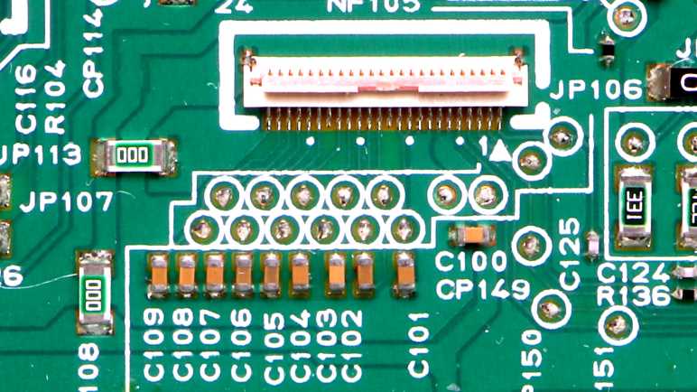
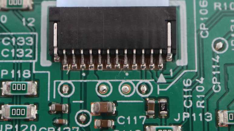
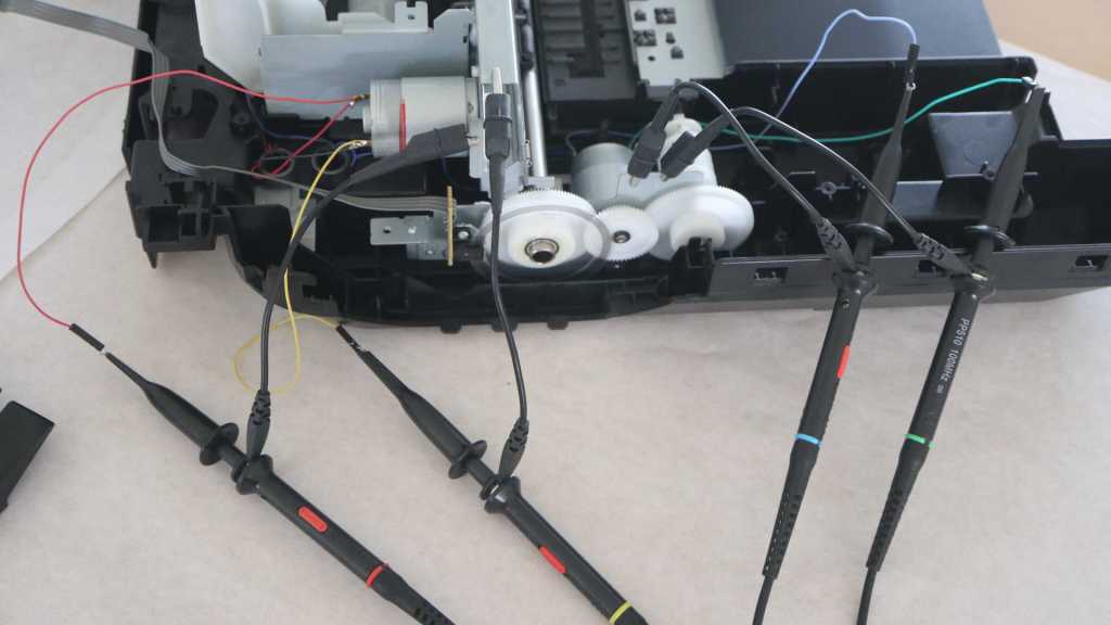
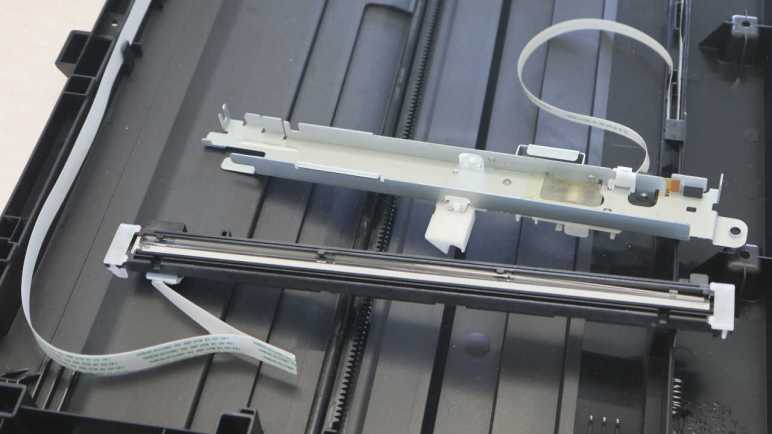
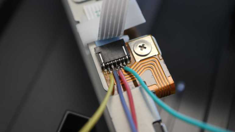
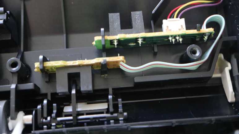
Poking around internals of a retired Canon Pixma MX340 multi-function inkjet, I decided its control panel circuit board was within my skill level to decipher. After following a set of five wires from control board LCD screen to the biggest chip on the board, I think the next effort is to trace out the relationship between that chip and all components on this circuit board. I started doing this by eye but the traces are thin, the contrast is low, and my eyesight isn’t what it used to be. If I will be tackling many more similar projects, I might invest in a magnifier or microscope designed for circuit board work. But for today, I’ll use what I already have on hand: taking pictures with my camera + macro lens then stitch them together.

In order to keep the circuit board traces as well as surface component markings in focus, I need to narrow the aperture for greater depth of field. I also wanted to use my polarizing filter to eliminate glare. Both decisions reduced the amount of light reaching my camera sensor. To compensate, I can increase sensitivity, but that adds noise and I don’t want a noisy picture when looking at fine copper traces. The alternate solution is to increase shutter time, which meant setting up my tripod to keep my camera steady during long duration shots. I ended up using an 8 second shutter time in order to stay at low noise ISO 100 sensitivity.

For each picture, I wanted to fill my imaging area with circuit board. The aspect ratio of the circuit board meant I could cover the entire width with four pictures. However, that means a seam somewhere in the middle where all the important bits (main board connector, LCD connector) are located so I decided to take five pictures. One center shot with all the important bits together in one shot, then two pictures on either side.

Once I had the pictures, I brought them into my photo editor putting each image into its own layer. I brought the center image to the foreground, the edge most images to the back, and intermediate images between them. I then scaled image in each layer so all the copper circuit traces lined up at the edges. Looks like I didn’t manage to maintain distance between camera and circuit board, because this resulted in a slightly trapezoidal shape.

After the traces were all lined up, I adjusted image color levels to bring out contrast of copper circuit traces. Doing this meant blowing out bright parts and dark details got crushed, but I decided that’s not important for this project. I also decided not to worry about the fact seams are very noticeable, because color balance changed between pictures.

I didn’t use panorama photo stitching software here because they have different goals. They fix color balance, warp perspective, and blend edges to create a pretty picture. For this project, I’m not looking for pretty, I’m looking for accurate. When I’m following a copper trace across the board, I want to be confident I’m following real untouched data and not misled by something that had been modified to look pretty.

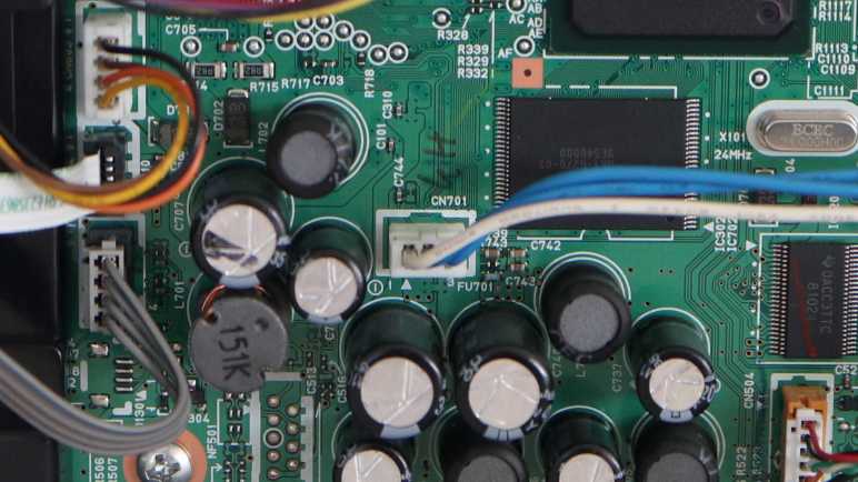
Here is a low-resolution version of the result. If anyone else wants a look, the full resolution version (and original set of five images) are up on my GitHub as they are too large to be hosted here. Obviously I’ll use the full resolution version for further circuit board exploration.


This teardown ran far longer than I originally thought it would. Click here for the starting point.

Canon Pixma MX340 Control Panel LCD to IC

I’m examining the control panel circuit board from a Canon Pixma MX340 multi-function inkjet to see what I can learn. After identifying all but five LCD screen connector pins, I’m obviously inclined to follow those five pins. Again, I took the best picture I could and edited the photo to highlight traces and make them easier to follow. The good news is that all five wires traveled together to a conspicuous feature on this board: a row of five resistors marked 331 for 330 ohms.

I noticed this row of resistors in my initial cursory examination and had been curious to their purpose, now they’ve been moved to the top of the queue. One bit of oddity that caught my attention was the fact their marking numbers didn’t all align the same way: three were installed one direction, and two the other. I’m pretty sure they would have been all in the same orientation from the product reel, yet the pick-and-place machine decided on different orientations. While the orientation doesn’t matter for resistor functionality, there must have been a reason to not do the same thing five times and I wonder what it was.

Between each resistor and the LCD connector, each wire also has a capacitor to ground. (C123-C127 inclusive.) C124 is also accompanied by R136, which looks like a pull-down resistor. There were no other features I could see, aside from test points labeled with the CP prefix. “Check Point”, maybe? On the other side of the resistor, all five wires were routed under a few zero ohm resistors labeled with the JP prefix (probably meaning “jumper”) and went under the biggest (only?) chip on this circuit board.

The chip is marked NEC K13988 1022MM1H. A search for this designation found several electronic component distributors offering to sell some to me. I checked two of those links: neither actually had the chip in stock, and both used a placeholder image instead of a picture of the actual chip. More importantly, while both pages had a “Datasheet” link, they didn’t link to a PDF. Instead, they were links to different datasheet dump sites, both of which helpfully offer “Here are some datasheets for components starting with K139…” none of which was K13988 and none were made by NEC.

Without a datasheet, I’ll have to infer this chip’s functionality. This is a 30-pin part mounted on a single-layer board serving a known purpose, so this should be a tractable problem. In addition to normal power and ground wires, there are the five pins for communication with the LCD. A few pins would be routed to the cable connector to communicate with the main board. Some of the pins are likely used as outputs to indicator LEDs, but there’s a small chance the main board directly handle all LEDs. (There are only a few of them.) The rest would be used to read button status, likely with a row/column matrix of wires.

To find these answers, I’ll need to follow copper traces over much longer distances, possibly across the entire width of this control panel circuit board. I couldn’t do this by eye because the contrast is too poor for me to follow narrow traces. I need the photo editing contrast enhancement. But if I pull my camera back far enough to encompass the entire board, those narrow traces become too blurry. I’ll have to take multiple pictures and stitch them together.


This teardown ran far longer than I originally thought it would. Click here for the starting point.

Canon Pixma MX340 Control Panel LCD Connector

I have a Canon Pixma MX340 multi-function inkjet in a partially disassembled state, still running, and I’m learning how it works. Looking at the control panel, I was encouraged by how much I could learn just by looking at the connector to the main board, so I will keep going and look at its LCD screen connector.

The first challenge is the LCD interface connector is even smaller and denser. My experience had been hobbyist-level electronics for a breadboard with pins 0.1″ (~2.54mm) apart. The main board connector had just 1mm between pins, over double the density. This LCD connector doubles density again, with only 0.5mm between pins. Those thin copper traces were hard to see so I took my picture and exaggerated its contrast. Bright parts are now overblown and dark detail crushed, but the traces are much easier to see now and that’s what’s important today.

Since Canon engineers thoughtfully labeled pin 1 with an arrow and number, I know to count pins right-to-left. The first thing to do is look for traces larger than the rest, usually indicating power/ground wires. I see three instances of two pins wired together: 6+7, 8+9, and 10+11. Visually following the copper traces, I found LCD pins 6+7 connected to mainboard pin 9 that delivers 3.3V even in standby mode. LCD 8+9 is connected to mainboard pin 10, the curiously thin ground pin. (LCD draw very little current, so that is consistent with the hypothesis pin 10 serves low power draw components.) C100 is the decoupling capacitor between those power and ground planes.

LCD pins 10+11 didn’t go very far: they led to capacitor C101, the other side of which is ground. In fact, looking at that patch of copper, five more capacitors (C105 through C109 inclusive) connect corresponding LCD pins (19 through 23 inclusive) to ground. Working towards the right, C104 sits between LCD pins 17 and 16. C103 between LCD pins 15 and 14. C102 between LCD pins 14 and 13. I’ve seen LCD modules use external capacitors before, but this is a much larger capacitor network.

I don’t see any traces going under the connector out the other side, so pins 12 and 18 are either unconnected or connected to one of the copper patches that run under the connector. One patch is ground, to which the connector’s chassis pins soldered to. There’s a smaller patch, which supplies power to pin 24.

This tiny super dense connector was intimidating at first glance, but as it turned out an explanation can be found within 3cm for majority of those pins. Only 5 pins out of 24 require further exploration.

[UPDATE: I now have information on pins 1 through 5, which connects to NEC K13988 chip on the circuit board. Table has been updated accordingly.]

Pin numberConnection
1NEC K13988 pin 28
2NEC K13988 pin 26
3NEC K13988 pin 27
4NEC K13988 pin 9
5NEC K13988 pin 10
63.3V DC
73.3V DC
8Ground
9Ground
10C101 to ground
11C101 to ground
123.3V, ground, or not connected
13C102 to 14
14C102 to 13 and C103 to 15
15C103 to 14
16C104 to 17
17C104 to 16
183.3V, ground, or not connected
19C105 to ground
20C106 to ground
21C107 to ground
22C108 to ground
23C109 to ground
243.3V DC

This teardown ran far longer than I originally thought it would. Click here for the starting point.

Canon Pixma MX340 Control Panel to Main Board Connector

I have the front control panel of a Canon Pixma MX340 multi-function inkjet and I will try to understand of how it worked. I’m starting with this 12-pin connector for the ribbon cable leading to the main board, because all input and output will necessarily go through this connector. Luckily this circuit board only has a single layer of copper traces. Making it much easier to glean information just by looking at the connector and its immediate surroundings.

The first piece of good news is the fact Canon engineers had drawn an arrow with a number 1 in white silkscreen on the board, sparing me the agony of trying to guess which pin is #1. Using that numbering system, the first circuit observation is that pins 4 and 8 are visibly connected together immediately adjacent to the connector. Pins 5, 6, 7 must go under the connector out the other side, something I’ll track down later.

Having multiple pins connected together with large sections of copper (instead of thin traces) usually indicate multiple pins connected to a common ground. Probing with my multi-meter I confirmed those two pins showed only about a single ohm of resistance to the metal chassis. But the “ground wires are big” is only a rule of thumb, because I probed the remaining pins and found pin 10 — a thin trace typical of data signals — is also connected to ground. I assume it is part of a circuit with low power draw so it doesn’t need a fat low resistance ground wire.

The next circuit observation are the capacitors right next to the connector, sitting between the just-identified ground wires and three other wires. This is typical pattern for decoupling capacitors and imply those other wires — pins 3, 9, and 12 — are power supply wires. Probing with my multi-meter while the printer is turned on, pins 3 and 9 read 3.3V and 5.5V for pin 12. I then repeated the probe with the printer in standby (“turned off”) state, and saw pin 9 still had 3.3V while the other two has dropped to zero. Implying certain parts of the board stay active even in standby state while the rest of the board is powered down.

Pin 3 has a resistor adjacent to its decoupling capacitor. Marked with “471” indicating 470 Ohms. That is a popular value to use as LED current-limiting resistor when connected to 5V DC. This wire gets 3.3V instead of 5V but that should still result in more than enough current to illuminate a modern LED. When I trace through the circuit later, I will find out if this is a LED illuminated directly by the main board or if the familiar 470 Ohm value is only a coincidence.

With this basic exploration, I already have tentative information on half of the pins. [UPDATE: This later post has filled in the rest of the table.] This is a very encouraging start and motivated me to go look at the other connector on this board, for its LCD screen.

Pin NumberTentative GuessPrinter OnPrinter Standby (“Off”)
1?
2?
3Maybe LED power?3.3V DC0V DC
4Ground
5?
6?
7?
8Ground
9Always-on power3.3V DC3.3V DC
10Ground
11?
12Power5.5V DC0V DC

This teardown ran far longer than I originally thought it would. Click here for the starting point.

Canon Pixma MX340 Control Panel Round 2

After looking at the paper feed roller shaft position encoders of this Canon Pixma MX340 multi-function inkjet, I don’t have too many other circuit boards to probe. But the remaining boards are significantly larger like the user control panel. I took a quick look at this earlier during mechanical disassembly, now I want to look at it electrically.

Thankfully, it is large mostly because it spaces things out for user-friendliness.

The circuit board only has a single layer of copper traces. Most of the components on the non-copper side are push buttons. There are a few LEDs, and a few jumper wires to help route signals over backside copper traces.

Electrically speaking, this board needs to read the state of all the push buttons and report them back to the main board. It is also home to a bitmap LCD screen, displaying information on command from the main board. Plus the on/off state of those LEDs. All main board communication occurs over a small ribbon cable with 12 conductors.

Functionally, this serves a similar purpose to the front face plate of a car audio system. I’ve looked at two units earlier, one from a Toyota and another from a Honda. Both of them used chips from Sanyo designed to perform both tasks (button matrix scanning and driving the LCD) on behalf of a main board via an electrical connector with roughly a dozen or two of conductors. Like those face plates, only a single significant looking chip resides on this printer control board. Perhaps it serves a similar purpose.

Before I dive in to that chip, though, I thought I would first explore around it. This is another lesson learned from those car faceplate teardowns: it is common for a few electrical conductors to be reserved for direct main board control bypassing that chip. If such direct connection wires are among the 12 conductors of this cable, knowing where they are would make later analysis easier. I’ll look at that connector first.


This teardown ran far longer than I originally thought it would. Click here for the starting point.

Canon Pixma MX340 Paper Feed Shaft Encoder

I’m poking around inside a Canon Pixma MX340 multi-function inkjet and was surprised when my oscilloscope showed it rapidly cycled between forward and backward power to its two DC motors. I’m sure it is related to the fact they’re part of a closed-loop control system: the printer has high-resolution encoders telling the mainboard how much each axis has moved, so the control system can adjust the forward/back power ratio.

I can see the encoder strip used for the print carriage, but the encoder itself is not easily accessible. The data wires would be among print cartridge control wires somewhere in the trio of cables between print carriage and main board.

In contrast, the paper feed encoder is a standalone unit with only four wires already conveniently labeled 1 through 4 from left to right in this picture.

It looks like the encoder has some sort of physical pad to keep the encoder disc properly aligned in the channel. It has worn a groove into the plastic encoder disc and will eventually wear through and destroy the disc. But it lasted long enough for me to retire the printer first, so “It’s not just good, it’s good enough!

Since physical position and alignment is clearly important here, I didn’t want to remove the module while I still want to probe the system in a functioning state. It looks like a pretty simple one-layer circuit board. Aside from the cable with four wires (1 through 4 from right to left, now that we’re looking on the back side) and the encoder sensor itself, there are two surface mount components. One looks like a capacitor, and other looks like a small resistor marked with either 820 (82 Ohms) or 82D (629K as per Digi-Key tool).

It was a tight fit to get my soldering iron into that space, but at least the four wires were generously spaced apart so I could solder wires for attachment to oscilloscope probes.

This is again from the power-up sequence, when this motor is running backwards. This matches the wave form I expected to see from an incremental encoder. Unlike the photo interrupter sensors that ran at 5.5V DC, this encoder runs at 3.3V DC. The shape of the curve, tapering off as rose up to 3.3V DC and a sharp drop with no taper when it goes to ground, tells me there’s a pull-up resistor on each line and the sensor itself pulls to ground.

For comparison, here’s the plot from later in the power-up sequence, when the motor is running forward but at a slower speed. The red/blue ordering is reversed, and the pulses are wider apart. I’m curious about the slight voltage drop I see in one color when the other signal is pulled to ground. Is this caused by interaction between the two pull-up resistors or something else?

The pinout for this sensor can be determined from these oscilloscope plots. As per numbers printed on the board: pin 1 is 3.3V DC, pin 4 is ground, and A/B phase signals live between them.

That was a nice simple circuit board to decipher, the next project is a little more complex.


This teardown ran far longer than I originally thought it would. Click here for the starting point.

Canon Pixma MX340 Motors for Print Carriage and Paper Feed

When I started taking apart my old Canon Pixma MX340 multi-function inkjet, I didn’t expect to make heads or tails of the sensor bar. So I was very proud of myself for getting far enough with a reasonable hypothesis on how to work with it, and jotted down some potential approaches potentially scaled down to my skill level. They are potential projects for later. Right now I want to move on with observing other parts of the machine. Today’s subjects: the motors used to move the print carriage horizontally (“X-axis”, in my mind) and a separate but similar motor responsible for feeding sheets of paper (“Y-axis”).

There are two wires on each motor, characteristic of inexpensive commodity brushed DC motors. I was pretty confident I knew what I’ll see on my oscilloscope screen: 0V ground on one wire and 24V DC from the power supply on the other wire in a PWM pattern depending on desired speed. It turns out I was both right and wrong.

There’s definitely PWM going on, but in both directions! Here’s the oscilloscope plot for the print carriage motor upon startup, moving the print carriage out of its parking spot across the width of the printer. For slow motion I expected a low PWM cycle on one pin and the other pin held kept at ground, but the printer actually alternates between turning the motor forward and reverse with no de-energized states between them. (Not counting the very brief MOSFET ramp-down during the switch.) I guess this is similar to how when we want to make precise motions with our limbs, we keep some tension on muscles on both sides of the joint. The motor speed is thus dictated by the ratio of time spent in each direction.

Continuing the startup sequence: After the print head moved across the entire width of the printer, it moves back towards its parking position at the same speed. Changing the edge trigger channel made it easy to see the same ratio was used except with the polarity reversed.

The paper feed motor is driven in a similar manner. This was also taken during the printer startup sequence, at the moment the motor is spinning in a direction backwards from normal paper feed direction during printing. I don’t know what this motion accomplishes yet, I hope to find out later in this teardown.

Shortly after that action, the motor turned in the normal paper feed direction for a short distance. (Not far enough to pop open the paper output tray door.) It also turns at a slightly slower speed. The most obvious difference between these two plots are the different in voltage for opposite direction, and a less obvious difference is the power energized ratio between blue and green wires. It is slightly closer to 50/50 when the motor is turning slower.


Driving the motor in this manner is not very energy-inefficient, as most of the power is spent fighting power expended a few microseconds earlier. Only a fraction actually goes into motion, all the rest are turned into heat. Indeed these motors grew warm to the touch after some use. There’s probably an explanation for why this is the preferred approach, somewhere in an electrical engineering motor control theory textbook. Maybe this is the only way to reliably accomplish precise movements with inexpensive DC motors? I should experiment with this concept the next time I revisit my micro Sawppy project, perhaps it would allow the little thing crawl at a more rover-like speed. However, I think it’s likely this motor control scheme only works because it has encoder feedback for a closed-loop control system.


This teardown ran far longer than I originally thought it would. Click here for the starting point.

Canon Pixma MX340 Scanner Image Sensor Partial Reuse Ideas

Thinking over what I now know about the scanner image sensor bar from a Canon Pixma MX340, I’ve decided using the sensor properly is beyond the reach of my current electronics projects skill level. My biggest problem is that I don’t have the tools/skills to keep up with a data clock signal running at 2.375MHz. But what if I just ignore that clock signal? For digital data, ignoring clock pulses would mean we just get gibberish. But this sensor bar communicates image data in analog voltage values. Theoretically, it is a valid option to sample that analog line at a lower rate to obtain a lower resolution image. The “new line is starting” pulse is still there at 425Hz to separate one line from the next, and keeping up with a 425Hz signal is a more tractable problem if I can get the analog sampling side figured out.

Arduino (ATmega328P)

Can an old school Arduino Nano on a ATmega328P chip keep up with the 425Hz line sync signal? I don’t know. Suppose that it could, the analog sample limit of 10k/second means (10000/425=) 23-ish samples per line or (23/8.5)=2.77 dots per inch. That’s worse resolution than a row of photo-resistors and probably not worth the effort.

ESP32

How about the ESP32 chip? It’s a much faster processor but higher core processing speed doesn’t necessarily correlate with faster ADC peripheral performance. I found this page Working with ESP32 Audio Sampling describing one effort to run the ESP32 ADC at high speed. This particular author found ESP Arduino layer to be limiting and went deeper to make some ESP-IDF calls directly.

Audio Hardware

That page got me thinking about hardware peripherals that sample an audio signal. Unlike high speed ADC chips for the industrial market, an audio-in peripheral is something available to the hobbyist market. Audio sampling usually tops out at either 44.1kHz or 48kHz, and has the advantage of being tailored for consistent performance at that sampling rate. Another advantage of the scanner image sensor pretending to be a microphone is that it’s pretty common for audio ADC to measure signal relative to a base reference ground, something I can take advantage of with the sensor pins.

The challenge of using an audio-in peripheral is splitting the incoming “audio” sample data into lines using the 425Hz line sync signal. At the moment I have no idea how I’d go about it.

I2S ADC Mode

One common protocol for communicating audio data to/from an external peripheral is I2S. Not only does ESP32 support the I2S protocol, its I2S hardware peripheral can be adapted to other high speed signal tasks unrelated to communicating audio data. At one point, Espressif offered a way to use the I2S peripheral to transfer data directly from ADC peripheral to memory at high speed. (A maximum sampling rate of 150kHz, as per old documentation for i2s_set_adc_mode.) Unfortunately, they’ve since moved i2s_adc_enable, i2s_adc_disable, and related APIs off to the “legacy” portions of ESP-IDF. The latest ESP-IDF documentation only has a short paragraph acknowledging it once existed and spoke no more of it.

Even if it was still a supported API, I saw several complaints on the ESP32 forums that the ADC is very noisy. Something I’ve found out firsthand, and apparently that limitation gets worse as we go faster. Looks like using ESP32’s onboard ADC peripheral wouldn’t be a great way to go, suggesting an external peripheral. I’ve already determined it’s not really practical to get those high-quality high-speed industrial ADCs, but maybe another microcontroller has better onboard ADC peripherals?

STM32

Searching for discussions on microcontroller ADC, I found references to chips in the very large STM32 family of products. Some have superior ADC capabilities, at least on paper. The most promising lead is ST Application Note AN5354 Getting started with the STM32H7 Series MCU 16-bit ADC. Figure 1 shows ADC behavior while sampling at 16-bit in differential mode @ 2.5 million samples per second. That’s the kind of speed needed for the scanner sensor bar!

And what’s this “differential mode”? I found a ST forum thread ADC input voltage range in differential mode where the explanation says it is a STM32 configuration using two hardware ADC channels together. The hardware will generate a single data stream from the difference between them. In other words, exactly what I want to evaluate signal+ against signal- voltage levels. Even better!

This sounds perfect. but I don’t know how the STM32H7 chips relate to the STM32F103 chips commonly available to hobbyists as the “Blue Pill” board. This is something I will need to research. I knew the “Blue Pill” is very popular with some circles of electronics hobbyists, and I’ve had requests for a STM32 Sawppy brain. If I try to do build a project around this Canon MX340 scanner sensor, it might be the motivation I need to get into STM32 development. But that’s far too big of a project for me to undertake as a side detour, so I’m going to set that aside and resume examining the electrical behavior of this inkjet. Next up: the DC motors.


This teardown ran far longer than I originally thought it would. Click here for the starting point.

Canon Pixma MX340 Scanner Image Sensor Reuse Challenges

I’ve examined the scanner image sensor from a Canon Pixma MX340 multi-function inkjet while it was still attached and running. I think I now understand how it communicates with the printer main board. However, that’s a ways from being able to reuse the sensor in my own electronics projects.

The first obstacle is that I only know voltage levels on the wires, I don’t know which component (the sensor or the main board) was responsible for putting them on the wires. Some are easy guess: the LED illumination power must come from the main board, and the image data must come from the sensor. But others are ambiguous: I see a clock signal, but who’s generating it? In order to reuse this sensor, I need to know what I need to re-implement in my own circuit in order to impersonate the printer main board.

The second obstacle is speed. My oscilloscope measured that clock signal at 2.375MHz. If my project is responsible for clock, toggling a pin in software won’t be fast enough and my current hardware skills can’t build an appropriate oscillator circuit. On the upside, if my project would be responsible for generating the clock signal, perhaps I can emit a slower clock and make everything easier. Of course, that’s out the door if clock was sensor-generated and I have to keep up. A dedicated hardware peripheral may be needed. 2.375MHz is a challenging speed for microcontroller code to keep up, demanding at least an interrupt-driven system if not other performance techniques.

Another speed-related challenge is reading and processing the analog pixel brightness value. Analog-to-digital (ADC) conversion is a common peripheral feature in many affordable microcontrollers, but they can’t sample data as fast as 2.375MHz. The basic Arduino boards built on the ATmega328P chip has a limit of 10k samples per second, two orders of magnitude too slow. That seems to be the typical ballpark for hobbyist-level hardware. Looking over Adafruit selection of ADC modules, it looks like item #5836 is the fastest unit which traded precision for speed, but that’s still only 70k samples per second.

High-speed ADC modules certainly exist, available with capabilities up to billions of samples per second. I found many listings from companies like Texas Instruments and Analog Devices. (Very appropriately named in this context.) But they’re not the kind of chips Amazon/AliExpress vendors put on breadboard-friendly breakout boards.

Given these challenges, reusing this sensor to its full potential is currently out of reach for my own projects. However, the data signal is an analog signal, and the beauty of analog systems is that we have the option of a partial (a.k.a. half-assed) implementation.


This teardown ran far longer than I originally thought it would. Click here for the starting point.

Canon Pixma MX340 Scanner Image Sensor Pinout

Taking apart a Canon Pixma MX340 multi-function inkjet, I wanted to see what I could learn from its scanner’s CIS (contact image sensor) bar. Expectations weren’t high at the start but after spending some time looking at its behavior under an oscilloscope I think I understand enough to explain every pin on its cable connector.

I’m arbitrarily numbering these pins from left-to-right in this picture. I don’t have Canon’s electronic schematic or engineering data, so this might be reversed from Canon’s actual pin ordering. I feel confident about the accuracy of red labels, I’m more tentative about the pins labeled in blue.

The first five pins support illumination. There are separate pins for red/blue/green LEDs and they all shine onto a common light guide that disperses across the sensor bar.

  1. 5.5V DC power source as common LED anode.
  2. Red LED cathode.
  3. Green LED cathode.
  4. Blue LED cathode.
  5. Chassis ground.

The remaining seven pins support image sensor data.

  1. Data clock (tentative) at 2.37538MHz with amplitude of 3.3V. Clock signals are normally square waves. This one is very nearly a smooth sine wave but I guess it still counts?
  2. Line sync+ (tentative) at 425.543Hz. Raised up to ~3.3V for one data clock cycle to signal new scan line, read on falling edge of clock signal. Low voltage level fluctuates relative to chassis ground, but is in sync with line sync- and should be compared against that.
  3. Line sync-. Reference base for pin 7 line sync+.
  4. 3.3V DC power source for image sensor logic.
  5. Power ground for image sensor logic.
  6. Analog pixel data+ (tentative). Raised up to ~3.3V above chassis ground (or roughly 2V above reference base pin analog pixel data-) to indicate brightly lit pixel. Drops to less than 0.1V above reference base for both dark pixels and overblown pixels. Drops under reference base in the non-data periods at the beginning and end of each scan line.
  7. Analog pixel data- (tentative). Reference base for pin 11 analog pixel data+. Voltage level is roughly 1.0V above chassis ground but fluctuates in sync with analog pixel+ approximately +/- 0.1V.

All of this information were inferred from using either a multimeter or an oscilloscope to observe voltage levels on each pin, while the printer is either going through its startup sequence or sitting idle. This doesn’t tell us which component is responsible for which signal. For example, while pin 11 analog pixel data is certain to come from the sensor bar, this data doesn’t tell us if the clock signal on pin 6 comes from the sensor bar or from the printer main board. That’s just the first of many barriers against repurposing this sensor bar.


This teardown ran far longer than I originally thought it would. Click here for the starting point.

Canon Pixma MX340 Contact Image Sensor Signal

I have a contact image sensor (CIS) from the scanner module of a Canon MX340 multi-function inkjet. Connecting its wires to my oscilloscope, I found a wire that I believe to convey image data.

The yellow line is probably the clock signal, and the green line fluctuates in rough correlation with sensor light levels. When the sensor bar is facing down, the signal hovers near lower voltage levels. When it is facing up towards the light, more of the signal line shows at a higher voltage. I think this is the “analog” output format for Canon contact image sensors!

If the yellow line is indeed the clock signal for each sensor pixel, and the voltage level is an analog representation of the brightness of that pixel, there is still one missing piece of data: how would we know when a scan line had completed and another begins? There must be a signal on one of the other wires, and I know there’s something that occasionally flashes past this screen. Time to chase that down.

Playing around with the oscilloscope trigger, I eventually pinned the flashing culprit down to the red wire. Its voltage is raised high for a single clock cycle at a rate of 425.543Hz. Dividing the frequency of the yellow clock signal (2.37538MHz) by 425.543 yields 5582 yellow clock cycles per red cycle. The scanner bed is 8.5 inches wide, so 5582/8.5 ~= 656. This would make sense for a 600dpi image scanner bar that is slightly wider than the scan bed.

This oscilloscope plot also shows the red signal wire voltage looks wavy, but not when compared against the blue signal wire. I think these two voltage values are intended to be evaluated together: the “new scan line” signal should be evaluated as red voltage minus blue voltage.

Keeping the oscilloscope trigger on the red wire, I changed horizontal scale to see a longer time duration. Lengthening the time scale 5000 times (from 100ns/grid to 500us/grid) showed scan lines represented by analog voltage. This particular plot shows three scan lines (one and a half scan line on either side of the trigger in the middle) and there’s a dip in the middle of each scan line. This is with the sensor bar looking up at the room ceiling so my finger is casting a shadow in the middle. I got excited that I could see some correlation between oscilloscope plot and light level, getting very close to understanding this sensor. But there’s a big problem: The shadow part looks pretty consistent, but the bright parts jump around wildly. Why is the data so noisy?

I lengthened the time scale again, by ten times to 5ms/grid so I could see about 30 scan lines at once. There’s definitely a pattern here, what is it?

Perhaps the fluctuation is normal? Since I just learned red wire voltage level appears to be relative to blue wire voltage level, maybe the image signal analog voltage is relative to another baseline. I moved the blue wire over to the pin adjacent to the signal wire to see if they fluctuate together in sync.

The good news is the baseline voltage hypothesis appears confirmed, with dark pixels dropping to the level of the newly relocated blue wire. These three scan lines show me holding my hand over the sensor bar, with several fingers casting shadows. The bad news is the non-shadowed areas are still fluctuating wildly.

I went back to staring at the earlier oscilloscope plot capture, trying to decipher a pattern to its repetition. The breakthrough came when I counted the period of repetition: at 5ms/grid, this is repeating every three grids plus a little more. So period of a little over 15ms, or a frequency somewhere under 66Hz.

Ah-Ha!

That was literally a light bulb moment: the image sensor bar is not only picking up the overhead lights, it’s picking up the 60Hz cycle of household AC power behind those lights. To test this hypothesis, I turned off my room’s overhead lights and switched to a battery-powered LED flashlight. The fluctuations disappeared, hypothesis confirmed! Now I feel pretty good about my understanding of this image sensor.


This teardown ran far longer than I originally thought it would. Click here for the starting point.

Canon Pixma MX340 Contact Image Sensor Connector

I want to see how much I can understand of the scanner image sensor bar I pulled out of a Canon MX340 multi-function inkjet. A little research side quest helped me feel better prepared for the task of figuring out what happens over the twelve wires connecting the sensor bar to the printer main board.

Looking at the copper traces on the circuit board, I can see some of them are directly wired to the pins for LED illumination. Verifying continuity between those connector pins and LED pins identified the left-most five of twelve wires. Probing for continuity with chassis ground, I found one more ground wire. Measuring the remaining wires while the system is powered up, I found one pin that held steady at 3.3V. A good power source candidate for image sensor logic.

That left five unknowns whose voltages fluctuate. Too quickly for my volt meter to catch what’s happening, hinting at data signals. My oscilloscope has four channels so I need to choose four to solder wires to and leave one for later.

This connector also has 1.0mm pitch and this time I managed to solder wires without creating bridges. Luck or improving skill I don’t know yet, either way I expect my MX340 teardown project will give me many more practice opportunities.

I turned on the MX340 and saw this on my oscilloscope screen. The yellow wire is attached to a pretty steady wave at 2.375MHz, possibly a clock signal. Its adjacent red and blue wires seem to track pretty closely to each other, the green wire looks much the same but at roughly 1V higher.

Unfortunately, that’s pretty much everything I got. I see this pattern as soon as the printer powers up, and it looks much the same during the homing sequence and afterwards. I waved my hand and shined a light at the sensor bar and saw no significant change in these signals. If I were looking at LVDS, according to Wikipedia I should see a 350mV change, but I don’t.

That said, there is something that occasionally flashes past this screen, but I didn’t know how to isolate it yet. Whatever it was, it occurred too infrequently to be image data. (Later I would determine it is a line sync signal on the red wire.)

Could the magical data wire be the fifth and final wire I had yet to examine? On paper it was a 20% chance I missed the most important wire, but Murphy’s Law raises those odds. Besides, I’m so close and it’d be silly to give up now. I turned off the printer and oscilloscope and turned on the soldering iron. The green wire was moved one pin over, and I tried again.

Jackpot! I have a candidate image sensor data signal.


This teardown ran far longer than I originally thought it would. Click here for the starting point.

Canon Pixma MX340 Scanner LED

I’m looking over the scanner module of a Canon Pixma MX340 multi-function inkjet. Its stepper motor got the oscilloscope treatment first, now onward to the image sensor bar.

When I took apart the scanner module, I noticed there were a few through-hole pins at the end of the image sensor bar and wondered what components they might be attached to. As I explored the scanner further to determine its startup behavior, I stared at the bar and saw the answer.

This end of the image sensor bar housed illumination light sources. This close-up shot showed the red, green, and blue LEDs working together to light the bar white.

From that I would expect three pins, one for each color, and a fourth pin as either a common anode or a common cathode. In actuality, I see five pins in this row. What did I miss? Starting with the basics, I probed the pins for continuity with chassis ground and found one, topmost in this picture.

I soldered wires to the four unknowns so I can see what they look like during printer startup, when the light bar is illuminated white looking for the homing marker.

Looks like the green wire is supplying 5.5V DC, possibly the same voltage plane powering the ADF paper sensors. The remaining three wires show a pattern that switches between two voltage levels and repeats less than 2.5 milliseconds. That works out to be less than 400Hz, too slow to be some sort of LED PWM scheme. Something else is going on. But first, I want to figure out if these wires are the positive anode (LED illuminates at higher voltage) or negative anode (LED illuminates at lower voltage).

I pulled out my LED tester and determined it is the latter: the LED illuminates from the 5.5V rail to the lower voltage shown on oscilloscope. I guess the ground pin is present merely for chassis ground and not actively used in this circuit. I also determined which wire corresponded to which colors, which is unfortunately now very confusing because I soldered these wires without knowing beforehand. Here is the mapping table:

Oscilloscope Wire ColorLED Color
YellowRed
RedGreen
BlueBlue

At least I got blue right.

Using this chart and looking back at the oscilloscope plot, I see each of the three colors are pulled low in non-overlapping time windows. The blue line (for blue LED) has the shortest time. Then the yellow line (red LED) with a slightly longer duration, and finally the red line (for green LED) for almost as long as the other two combined.

Why would the scanner light up one LED at a time and cycle through them? My hypothesis is this allows a monochrome image sensor to scan in color. Light up blue, scan. Light up red, scan again. Light up green, scan a third time. Assemble them together for full RGB color information. If so, the difference in LED illumination duration may be proportional to the image sensor’s sensitivity to those colors.

I am very happy with this discovery. It is already much further into understanding the scanner sensor bar than I had originally expected to get. Encouraged by this success, I want to see how much I can decipher of the rest of this image sensor. Which meant a quick side quest for contact image sensor research.


This teardown ran far longer than I originally thought it would. Click here for the starting point.

Canon Pixma MX340 Scanner Motor

I’m exploring the inner workings of a Canon Pixma MX340 multi-function inkjet as I take it apart. After coming up with a hypothesis on how the scanner bar finds its way to its home position, I had some fun confirming that hypothesis and confusing that electronic brain. Next I wanted to look at the motor that drives scan head movement.

Canon engineers designed the scanner bar to be easily disassembled into its two major components. A slight sideways push was all it took to separate the motor gearbox motion-control assembly from the lighting and imaging sensor bar.

Flipping the motion control assembly on its side, I can take a close look at the connector to a long cable leading back to the printer main board. There are five conductors in this wire, one of which went immediately to a screw fastening it to the stamped sheet-metal structure. This would be the chassis ground. The other four pins likely led to a pair of coils inside a stepper motor.

Probing those pins with a multi-meter, I found 15 Ohms of resistance between pairs of pins that I’ve labeled as +/- endpoints of two coils A and B.

This connector has 1mm spacing between pins (“pitch”) which is less than half of the 0.1″ (~2.54mm) pitch I’m familiar with. I’ve found this is roughly the limit of my current soldering skill, requiring two attempts before I could solder wires to them without accidental solder bridges. These wires were connected to my oscilloscope, measuring their voltage levels as the scanner went through its homing sequence.

This stepper motor is also run at 24V DC as delivered by the power supply, same as the ADF motor. The coils in this scanner motor measured 15 Ohms which calculates out to 1.6 Amps of current through each coil. Less than half of the power delivered to the ADF motor. And similar to the ADF motor, the scanner position motor does not need to hold position which means it avoids the high stress duty of having power continuously on a coil heating it up.

There’s a visibly repeating pattern in this oscilloscope snapshot, but it’s a bit difficult to make out each of the four wires when they’re all together on the same plot. Here they are individually:

Here are two ends of “A” coil, most of the time energized to one direction or another but there’s a brief period where both ends are at ground leaving the coil de-energized.

A similar pattern is visible in the B coil, offset by half a pattern period. I’m not sure why the motor cycle has this bit of de-energized coil time in between other energized patterns. Except for that small window, this pattern would be match what I expected from stepper motor operating theory. For a stepper motor spinning at a constant speed, I would expect something like this four-state cycle with equal duration per state:

A+B+
A+B-
A-B-
A-B+

But that’s not what I see in this oscilloscope trace. This is what I picked out, a slightly different pattern and some states are held for different duration.

A+B+
A+B-
A-B-
A-(off)
(off)B+

This difference from textbook description serves a purpose I couldn’t determine. Perhaps this helps ensure the coils don’t overheat from constant power? Maybe this is to help reduce resonance problems? Perhaps this is synchronized to the imaging sensor for some data purpose? It’ll stay a mystery for now, as I proceed to take a closer look at said imaging sensor.


This teardown ran far longer than I originally thought it would. Click here for the starting point.

Canon Pixma MX340 Scanner Homing Marker

I’m playing with a partially disassembled scanner module from a Canon Pixma MX340 multi-function inkjet. I’ve figured out how the scan head finds its way to its home position, and now I want to experiment with the marker used by the process. Back when I disassembled the scanner module, I had expected a mechanical homing switch but didn’t find one. I suspect the homing sequence uses a distinct pattern I found on the bottom of the bar separating the two windows.

Is this the homing marker? I will now confirm my suspicion.

The first experiment was to deliberately assemble the scanner module incorrectly. Instead of putting the lid (with glass windows) in its correct position, I placed it roughly 15cm offset in the positive direction. This was wider than the ADF window so the first test was a failure: the scan head didn’t move far enough before reversing direction. On the second test, I manually moved the scan head a bit further up, so the bar was in range of the initial positive scan. This time, the scan head homed to its new position. It also homed to the new position if I manually placed the scan head further in the positive direction: it would scan for a while, reverse direction, and find the relocated marker. Homing marker confirmed!

I then tried to see if I can spoof that marker. I measured the special pattern to start about 62mm from the document left edge. It is made of three black rectangles 20mm long and 3mm wide, separated by 20mm of white between them.

I drew up that pattern and printed it on paper. It took several attempts to actually match the measured dimensions because apparently “print at 100%” is a lie. I didn’t want to waste paper so my multiple attempts were printed on different ends and sides of the same sheet of paper.

Again I moved the scan head out of its homing position, and placed my fake homing marker paper down on the flatbed scan area. I turned on the printer and, when the scan head saw my fake marker, it acted as if it saw the real marker.

After this success, I realized that I had accidentally used one of the slightly smaller size fake markers. Retrying a few times with my different printing attempts, I found my 18mm and 19mm long markers worked just as well as the 20mm long markers. So the homing program has some tolerance for marker size.

If it is tolerant of less-than-perfect homing markers, perhaps I can spoof it with the pattern taped on a ruler? This worked when I put it on the flatbed glass like earlier experiments, but it failed if I skipped the flatbed glass and held the ruler on top of the sensor in midair. I can think of a few possible explanations:

  1. Holding the ruler above the sensor by hand had improper alignment. (It’s crooked.)
  2. Holding the ruler above the sensor by hand could not maintain the correct distance for proper image focus.
  3. The scanner sensor bar requires a sheet of glass between it and the scan subject for proper optical behavior.

And naturally, the explanation might be none of the above. I don’t feel the need to dig deeper right now because I’ve already had my fun and ready to move on to look at the motor moving this scann head.


This teardown ran far longer than I originally thought it would. Click here for the starting point.

Canon Pixma MX340 Scanner Homing Sequence

I’m carefully taking apart my old Canon Pixma MX340 multi-function inkjet, exploring its workings as I go. I’ve recorded the electrical parameters of the automatic document feeder (ADF) motor during printer startup, completing this phase of ADF exploration. My next focus is the scanner module, starting with the scan head homing sequence.

During power-up, there is a programmed sequence to ensure the scanner head is at its home position, sitting under the bar separating the small glass window (used for ADF scanning) and the large glass window for flatbed scanning. After opening up the scanner module, I could manually place the scan head at various locations to observe its homing sequence. I think I now understand how it works and writing it down here.

For the purposes of this description, I’m arbitrarily labeling the home position as zero. Movement towards the small ADF scanner window is in the negative direction, and moving down the flatbed scanner page is in the positive direction.

Usually, the scan head is already at the home position. It moves a little bit in the positive direction to verify it can detect its homing marker (more about that later) then returns to its home position.

If the scan head is not already at the home position, it will keep moving in the positive direction for a short distance. I measured this distance to be the roughly the size of the ADF scanner window. So if the scan head was located somewhere under the ADF scanner window, this motion should bring the homing marker into view.

If that short positive distance fails to detect the homing marker, the scan head reverses direction and runs for a much longer distance. I think this is the size of the large flatbed scanner window. So if the scan head was located somewhere under the large window at power-up, it will scan a bit in the wrong direction (thinking it might be under the ADF window) then course-correct back towards the zero position.

If the homing marker is not found after scanning in the negative direction for the size of the large glass, the printer enters an error state. Both its power LED and the “Alarm” LED will blink, and the LCD screen alternates between two messages: “Printer error has occurred” and “5011” which I assume is the error code indicating scan head homing failure.

It was fun to figure out how the scanner homing sequence worked, but it was even more fun to spoof that homing marker.


This teardown ran far longer than I originally thought it would. Click here for the starting point.

Canon Pixma MX340 ADF Motor

Working to understand the electronics of a Canon Pixa MX340 multi-function inkjet, I started with the automatic document feeder (ADF) on top of the machine and believe I’ve fully deciphered its paper presence sensors. Next objective is to measure the ADF motor’s electrical parameters.

Seeing four wires leading to the motor, I guessed it was a bipolar stepper motor. I disconnected its cable from the mainboard to measure resistance between each of these wires. I found two 8.8 Ohms pairs and open circuit in other combinations. This is consistent with the guess.

I didn’t find identifying labels around the perimeter. There might be something on the side facing the gearbox, but I didn’t want to disassemble it just yet.

The non-gearbox side is marked with QK1-6332 OXKT. Searching on that designation found a few eBay vendors selling replacement motors for a Canon MX340. This is oddly model-specific. I would have expected the same motor to be used across multiple devices. Perhaps this is not a designation for the motor but designation for a MX340 replacement part.

Taking advantage of the fact I still have a running printer, I soldered some wires onto the motor interface board to see their behavior during the printer’s startup sequence. The upper pair of wires (green and blue wires) is one of the 8.8-Ohm pairs, the lower pair (yellow and red) is the other pair. I expect to see four square waves alternating in a pattern consistent with driving bipolar stepper motors.

Here’s a snapshot of them during the startup sequence. Yep, bunch of square waves! I see the voltage level swings between 24V DC and ground, getting full power from the power supply. With 8.8 Ohm coils, straightforward Ohm’s Law calculation says the MX340 is driving this motor at 2.7A. Higher than I would have guessed, but within the range of power figures for a small stepper motor. It should also be noted that the ADF motor doesn’t seem to get powered on at a single coil for an extended period of time. Some stepper motor usage scenarios do this to hold position, but apparently not here. This is good because when power pulses are rapid and short in duration, the motor can tolerate higher amperage levels without burning out.

Isolating each of the wires, here’s the yellow-red coil. In the short time period of this snapshot, the coil is always energized one way or another.

And the green-blue coil doing the same. I’m not sure exactly what’s going on at the time of this particular snapshot, but it doesn’t have the regular pattern of a motor turning at a constant rate in a single direction. Perhaps I just happened to catch the motor as it switched direction? Digging for further details may be important if I am here to repair the document feeder. But as someone who only expects to repurpose the stepper motor in a future project, it is enough for me to confirm this looks reasonable for a bipolar stepper motor and knowing I can drive it at up to 2.7A at least for short periods.

That’s everything I wanted out of the ADF in this pass, I’m moving on to the scanner.


This teardown ran far longer than I originally thought it would. Click here for the starting point.

Canon Pixma MX340 ADF Sensors

I’m diving into the electronic guts of a partially disassembled Canon Pixma MX340 multi-function inkjet, starting from the top: the automatic document feeder (ADF).

Inside the paper feed mechanism is a pair of sensors that appear to be photo-interrupter switches.

I see a simple circuit board and through-hole components, so it looked like an easy starting point. There were no fasteners holding these two circuit boards in place, just cleverly shaped plastic molded into the body. A four-wire harness connects this sensor assembly to the main board. I see wires colored red, black, yellow, and purple. I guessed they would be power, ground, signal 1 and signal 2. (I was wrong.)

Here’s front and back of the sensor that senses when a document has been placed in the ADF. Looking at the back, I see a tiny surface-mount resistor labeled R51 and marked with “471” for 47 * 101 = 470 Ohms. This is a common value used for a LED current-limiting resistor, so that implies the associated pin is emitter LED power and the adjacent pin ground. Which makes sense, as it was routed to one of the pins of the receiver as well. Process of elimination says the final pin should be the sensor signal.

Turning the printer on, my hypothesis was verified with the volt meter. When light between the emitter and receiver is blocked, the sensor signal is at 3.3V. Probably pulled up by something on the mainboard. When there is no blockage between the emitter and receiver, the sensor signal pin is pulled to ground.

Given the 3.3 volts I detected on the signal wire, I had expected power to be 3.3V as well and was mildly surprised to measure 5.5V on that wire. Why go through the complexity of having multiple voltage planes? Maybe the engineers thought it would better to have higher voltage running through the long skinny wire from mainboard to sensor. But if so, why not use 24V DC directly from the power supply and use a bigger current-limiting resistor? 5.5V must present a useful tradeoff between 3.3V and 24V but I don’t know those Canon engineers’ considerations.

The other sensor detects whether a sheet of paper has been successfully fed into the ADF mechanism. It seems to use the same photo-interrupter sensor and the circuit works similarly.

Working back to the long 4-wire harness, I was surprised to discover my initial guess on wire assignments were backwards from the actual measured behavior.

RedBlackYellowPurple
ExpectedPowerGroundSignalSignal
ActualSignal 1Signal 2Ground+5.5V DC Power

I guess Canon doesn’t care much for wire color convention, where red is usually power and black for ground. Alternatively, maybe this was a production hiccup that inadvertently reversed the color order loaded on the wire harness machine. Maybe the relevant Canon engineering team decided: “Well, it is wired right electrically, so we’ll just ship with the wrong wire colors.” A valid choice! The end user never sees these wires and would never care about their color anyway. Maybe the story is documented in an errata for Canon technicians that I would never see.

That’s fine, I got what I came here for. Next up: the ADF motor.


This teardown ran far longer than I originally thought it would. Click here for the starting point.

Canon Pixma MX340 Cover Switch and Power Supply

I want to probe the electronic guts of this Canon Pixma MX340 multi-function inkjet and see what I can learn. Before I dive in, though, there were a few bits of preparatory work to be done.

There is a small switch in the device to detect if the cover (which includes automatic document feeder + scanner modules) has been lifted. This is usually a sign the user intends to either replace ink cartridges or clear a paper jam, so the printer goes into a non-printing standby state. It is spring-loaded to the open state. When the cover is closed, it presses on the lever and closes the circuit. In order to control state of this circuit without the weight of the cover pressing on the lever, I’m unsoldering its wires and moving them over to a large switch I salvaged from an earlier teardown.

I also wanted to see what’s going on with the power supply wires plugged into the mainboard. The label says 24V DC but there are three wires. From prior experience I expected them to be ground wire, power wire, and a signal wire to toggle low-power sleep mode. Thankfully, this connector exposed enough metal for my volt meter to reach them without fancy tools, and it was easy to probe the voltage level of each wire in the powered-up “ON” state and the standby “OFF” state. Looking on the circuit board silkscreen, I see this was designated CN701 and there’s an arrow pointing to pin 1, corresponding to the white wire.

Printer StatePin 1 (White)Pin 2 (Blue)Pin 3 (Blue)
On0.003.2424.21
Standby/”Off”0.000.008.50

Looks like pin 1 is ground, pin 3 delivers either 8.50V or 24.21V DC depending on the state of pin 2. The 3.24V I see on pin 2 in full-power mode is likely the logic high voltage, implying a circuit board primarily built around 3.3V DC components.

I also measured continuity (or at least minimal resistance) between pin 1 ground and the metal chassis. This will make electrical probing easier, because I can do things like putting oscilloscope probes’ ground reference alligator clip on the metal chassis instead of having to solder a separate wire to the circuit board ground plane. This was useful when I probed the automatic document feeder (ADF) sensors.


This teardown ran far longer than I originally thought it would. Click here for the starting point.

Canon Pixma MX340 Electronics Plan

I’m pausing mechanical disassembly of a Canon Pixma MX340 multi-function inkjet so I can explore its electrical aspects while everything is still running. I know I won’t understand everything and that is OK. Roughly in order of my self-confidence going in, the electrical subsystems I expect to find are:

Motors and Sensors: Yes

I expect to be able to understand all of the motors and mechanical sensors.

  • There are two stepper motors, one for the automatic document feeder and one for the scanner. Determine open-circuit resistance for their coils, and monitor the voltage they see during printer startup sequence. That should give me a ballpark figure of their electrical current capacity.
  • Determine pin-out of photo-interrupter sensors in this printer. This printer seem to use the same unit throughout, one that integrates the LED sender and the photosensitive receiver in a plastic package. Figure out which pins are power, ground, signal, and their voltage ranges.
  • Determine the typical voltage sent to the two DC motors, one for paper feed and the other for print head carriage. Since they are used in a closed-loop control system for precise positioning, I don’t expect them to see full 24V DC from the power supply.
  • Determine if pin-out of the paper feed motor’s encoder are power/ground/A/B as expected. Print carriage encoder is not currently accessible and will have to wait for later.

Control Panel: Hopefully Yes

I’ll take a look at the control panel, full of buttons and an integrated LCD. I managed to decipher the front panel of a Toyota tape deck and a Honda CD unit, and I’m optimistic that experience will help me understand what I will find on this front panel.

Scanner: Unlikely

While I’m pretty confident I can understand the stepper motor in the scanner, I’m less optimistic about the image capture side. A bit of web search found this Arduino forum thread, where I learned the imaging bar that moves across a scanner’s glass bed is called a contact image sensor (CIS). I haven’t found much in the way of publicly available documentation on any CIS modules. The prospects are even lower here because, as a worldwide leader in imaging technology, Canon probably produced this particular CIS for internal consumption. Meaning there’s even less reason for related documentation to be public.

I found a few YouTube videos that purport to cover all the things you can do to repurpose scanner components. They usually talk about the glass, the motor, the gears, the illumination light bar, etc. The sensor? “You’re not going to be able to reuse that.” Bah.

Maybe they’re right, but I’ll poke around anyway.

WLAN Module: Not Interested

I will ignore the Canon WiFi module, as I don’t foresee reusing that component. If I have a project idea that involves WiFi, I’m far more likely to pull out an ESP8266 or ESP32.

Ink Cartridges: Hell No

I will ignore the ink cartridges as well. I have a hard enough time understanding electronics without trying to untangle deliberate obfuscation. Ink cartridges are the profit center for inkjet manufacturers and encumbered with all sorts of trickery to discourage aftermarket ink cartridges. I’m going to steer clear of that mess.

Main Board: Examination Only

I’m interested in the motherboard only as far as looking it over for generalities. Try to figure out where the power handling areas are, identify peripherals like the stepper motor and DC motor control chips, stuff like that. Most of the components will be too small for me to reuse, and I’m not interested in trying to modify the firmware or running my own.


I think that plan is within my current capabilities, and I’ll start with the simplest things: a switch and power input.


This teardown ran far longer than I originally thought it would. Click here for the starting point.