Electric Blanket Control (Sunbeam PAC-215)

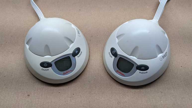
Electric blankets are an energy-efficiency way to stay warm during cold nights. If I’m going to stay in bed while sleeping, why heat the whole house? Heat just the bed and get a comfortable rest. But they don’t last forever, and this particular Queen-sized blanket stopped heating for unknown reasons. I’m going to take apart its two control units (one for each half of the bed) to see what’s inside.

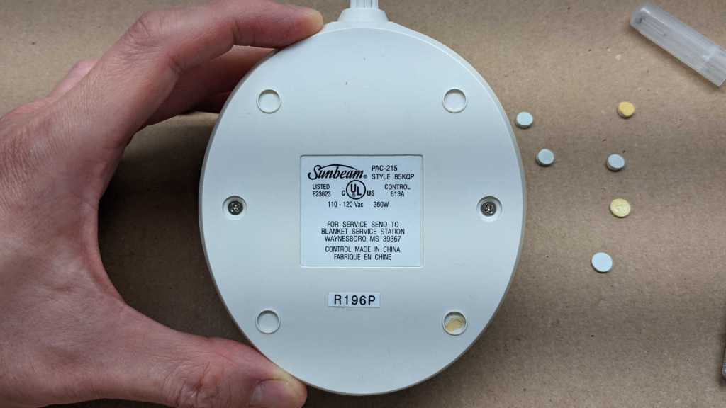
According to the label, this is a Sunbeam PAC-215 STYLE 85KQP with a maximum power draw of 360 watts. I interpret PAC-215 to mean the functional designation and 85KQP to mean a specific cosmetic variation, but that’s just a guess. (And it doesn’t affect a teardown, anyway.)

Peeling back all the adhesive circles unveiled two Philips-head fasteners.

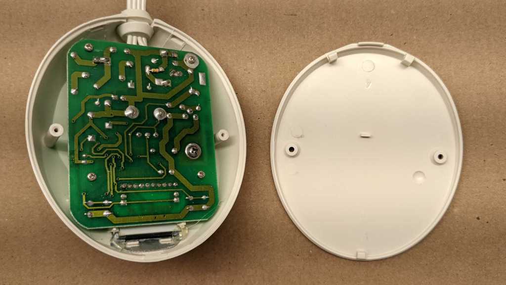
Once those two fasteners were removed, there were three plastic clips to undo before the bottom could be separated from the enclosure. We see many thick traces and wires of through-hole components. Four small Philips-head fasteners hold the circuit board in place, the larger fifth fastener is for the heat sink and can be left in place.

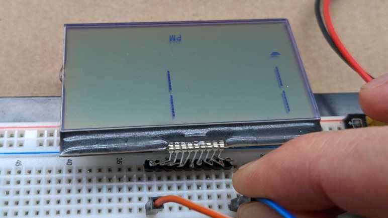
In addition to those four fasteners, the LCD is held by two plastic clips and blobs of hot glue.

Once removed, we could separate the circuit board from the enclosure. Curiously, I see a sheet of metal glued to enclosure top conducting from one of the four screws out to the front of the display area. It might be for grounding purposes, but there is no other metal for it to make contact. It’s not obvious to me what user scenario justified this effort.

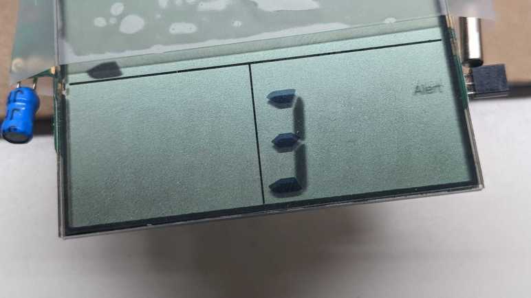
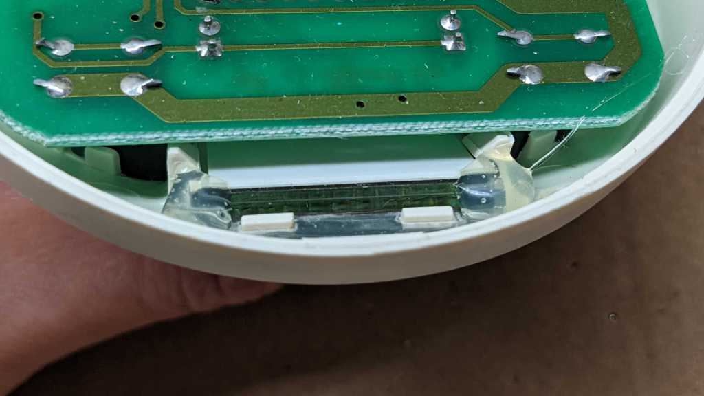
I was amused to see that backlight for the LCD is just a pair of LEDs soldered to the board. Simple, straightforward, and functional. No fancy multi-layer light diffusers for this screen.

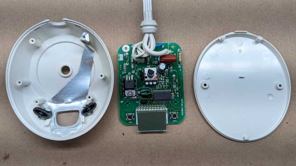
The circuit board has a white silkscreen marking of PEP003-0A.pcb on the left and a copper marking of FR4(94V-0) DD2 REVB on the right. This picture was rotated 180 degrees relative to earlier pictures to better read identifier on the large surface-mounted IC.
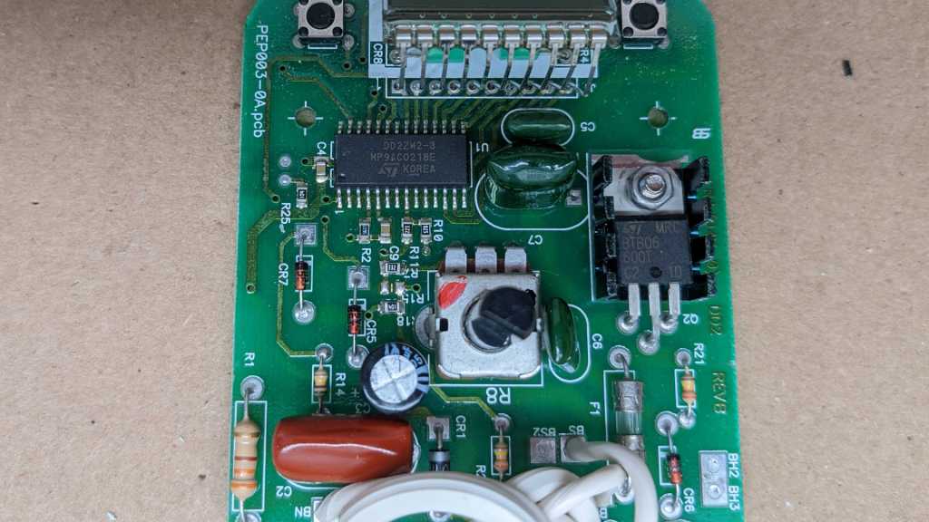
DD2ZW2-3
MP9ACO218E
KOREA

I can make out the ST logo but a search for “DD2ZW2” and “MP9ACO218E” on their site both came up empty. Based on the traces going directly to the LCD, this chip has LCD control capabilities. How much more? I don’t know. It might be a complete electric blanket controller solution for all I know. The other item with a ST logo is a BTB06 triac.

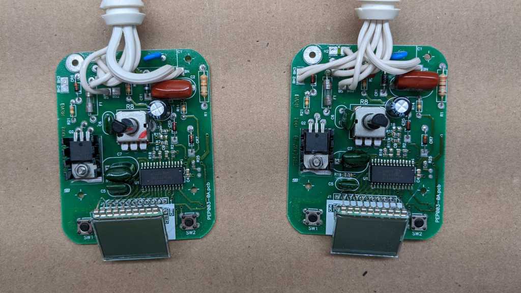
I then proceeded to disassemble the other controller, whose enclosure came apart the same way. I had expected to find two different circuit boards: a primary controller with majority of logic and a secondary unit purely for user interface purposes. I was wrong: the two circuit boards are identical. They only differ in how wires were soldered to each board. I followed their paths and drew a crude diagram.

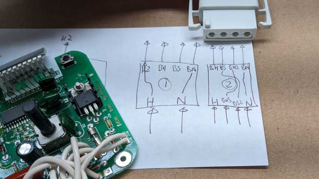
The power plug enters the first unit and connected to points labeled “H” (Hot) and “N” (Neutral). These are forwarded to the second unit as H2 and BN, respectively. H2 enters the second unit at its own “H” and BN goes to the second unit’s “N”.

Outputs of the first unit are labeled BH and BS, which enters the second unit as BH3 and BS2, respectively, and forwarded on to exit points BH2 and BS. The second unit’s own output goes out as BH, and neutral is forwarded out to the blanket plug.

The blanket plug itself was interesting. It was made of injection-molded plastic and designed to allow loose tolerances due to the flexible nature of the plastic yet still offer lots of mechanical strain relief.

The story continues inside, with plenty of strain relief considerations. This should nearly eliminate any mechanical stress from acting on the four crimped electrical connectors.

This teardown was more interesting than I had expected, as the controllers were more sophisticated than I had given them credit for. That was fun in its own right. But the motivation for doing this teardown today (instead of later) was so I could get my hands on some simple bare LCD modules I could play with.

Taylor Food Thermometer LCD First Round Fail

When I salvaged LCD for play later, I didn’t know enough about them to make sure I salvaged them with known controllers in working condition. Fortunately, by sheer luck I managed to do that with a car audio head unit. But this adventure started with a talk on direct control of simple LCDs and I wanted to get back to that initial motivation. My most recent LCD salvage was from a Taylor food thermometer, but it didn’t look easy to work with. Due to the fact its electrical contact is in the form of elastomeric “zebra strip” and I didn’t want to build my own circuit board to make contact with it.

I saved the original circuit board thinking that I could use it as reference when I get around to making my own board. These are just flat rectangles of copper, each one millimeter wide and spaced one millimeter apart. Thanks to Joey Castillo’s Remoticon talk, I learned that bare LCD require very little current so I think the surface area of these contact patches are generous. Perhaps I could get away with using only part of it?

I started soldering wires to these pads, trying to keep my soldered area to less than 25% of the surface area leaving remainder clear for the elastomeric strip.

I then severed all of the original traces to make sure my experimental signals won’t route through the original chip.

I started probing with alternating signals from an ESP8266 at 3.3V. This is what I see when I put them on the left-most and right-most wires: five segments darken, but one more clearly than the rest. “But wait, I see more than five segments” explanation: the three horizontal lines on that 3 are actually all a single segment, apparently this digit only needs to show a subset of numbers. For example, 2, 3, 5, 6, 8, and 9 can be shown with all three horizontal lines active, and 1 can be shown with all three inactive. There are four other dark segments but they are blurry. A horizontal segment in the upper left, two of the vertical segments on that digit, and a fixed text “Alert”.

Further probing found that the left-most five lines and the right-most five lines multiplex against each other, together letting me control 25 segments. Whenever I light one up, four others are blurry. After some experimentation I understand this is due to my voltage too high. Adding a voltage dividing resistor ladder (1 kilo-ohm and 470 ohm) brought it down to 2-ish Volts. Once at that level, individual segments activate cleanly without crosstalk activation of their multiplexing neighbors.

When I tried to get a picture of a single cleanly activated segment, I failed because a wire popped loose. Since this experiment required that I solder these wires to tiny fraction of the pad, these were very bad solder joints with small contact area. They began to fail one by one. Some would pop off cleanly so I knew it failed, others would seem to be physically connected but electrically discontinuous.

I got far enough to determine the multiplex scheme is different from the “common”/”segment” split mentioned in the Remoticon talk and common in multiple other LCD controllers. [Update: I was wrong. See link to update at the bottom of this post.] Figuring out the novel multiplex scheme might be interesting, but not while fighting bad electrical connections at the same time. After a few rounds of “multiplex or bad connection?” guessing game, I got frustrated and decided to postpone this puzzle until I can create better contact with the elastomeric zebra strip. I went looking elsewhere for a simple LCD.


UPDATE: I took another swing at this task and was successful on the second try.

Powering Up Toyota Audio Head Unit (86120-08010)

It appears two of my salvaged LCDs might have come from the same product, with identical (or nearly so) interface and command protocol. That is great, but I don’t know what that protocol actually is. It isn’t terribly promising as a starting point, so I decided to continue looking in my pile of salvaged electronics. Next candidate is the LCD embedded in the control panel of an automotive audio head unit. This was a stock tape deck from a 1998 Toyota Camry LE, which was replaced by an aftermarket deck for modern conveniences like Bluetooth audio. It was one of the retired pieces of equipment I brought to the January 2020 session of Disassembly Academy and taken apart. All metal pieces went into recycle, all plastic pieces went to landfill, and I kept the electronic circuit boards.

Since the metal external panels are gone, I no longer have the model number. Searching through eBay listings, I guess it was a Toyota 86210-08010. This listing explicitly mentioned Toyota Camry in their description. However, I saw several other Toyota units that looked superficially similar but with different numbers, like this 86120-04090. I thought maybe I’ll just call it “86210” but there are “86210” units that look wildly different like this 86120-2B761. Clearly there are complexities in Toyota parts numbering that I don’t understand, but for now I’ll go with 86210-08010.

The reason this particular LCD is interesting is because it is part of a still-intact control board. I’m optimistic that I could figure out enough of the control board to make it do my own bidding.

The backside of the board has a large identifier: 121941-4890D700. That didn’t turn up anything, but there are two other features on the back that make me optimistic.

The first is a clearly identified chip: Sanyo LC75853N and a search found its datasheet. It is a LCD controller with additional capability to scan for button presses, which makes sense for use in a control panel like this one. Furthermore, the datasheet should describe the control protocol.

Even better, the board has a connector to the rest of the radio, and it looks like all the pins are labeled. Some of them were cropped at the bottom and even if they weren’t cropped, I don’t necessarily understand what they all mean. But GND and ACC5V are clearly legible, which is a great start. What more can I ask for? Well, I can ask for it to be powered up and running so I can probe those pins in action.

When I replaced this head unit, I recall going online to purchase an adapter wiring harness and a pinout guide to know which wire went where. Many Toyota head units shared the same connector and pinout, so this diagram for a slightly different model was close enough.

I could buy another wiring harness, possibly this unit, but decided against spending more money. This is for experimentation and I could easily solder directly to the circuit board.

It probably didn’t matter very much in this case, but I also thought I’d follow wire color convention for automotive audio. I connected the “battery” (yellow) and “accessory” (red) wires up to +12V on my bench power supply, and black wires to ground.

The screen comes alive! Very nice. From here, I started disconnecting power wires and found that for purposes of powering up the control panel I only really needed half the wires, the three on the central connector. (Visible in the back of this image.) With a screen that is alive and kicking, and a datasheet that should explain everything, I expect a high probability of success for learning how to master this control board. This could be an interesting project, and the only problem is that it veers very far from Joey Castillo’s Remoticon talk which motivated me to look at LCDs. I set aside this project for later and started looking for simpler LCDs in my pile.


[UPDATE: I have returned to this device and made great progress on the second try.]

Risky Parallel LCD Test Surprisingly Worked

I briefly surveyed LCD controllers popular with hobbyist projects, hoping to find something that might match my mystery salvaged LCD units on hand. No luck. If my intention is to build a project with LCD screen, I should go and buy one of those popular units. But the point of the exercise is to try reusing salvaged electronics, so I stared at my two LCD units some more while thinking of Emily’s observation that they both had nine interface pins and the hypothesis they share a common command set.

I know for sure they aren’t identical. For starters, the two modules are different sizes. And while they both have nine interface connection; they are physically different. The bare LCD module has pins, and the headset LCD module is soldered to its circuit board with a segment of FPC (flexible printed circuit). Holding the bare LCD’s pins up to those soldered joints, I had an idea: what if I wired both LCDs together in parallel by soldering the bare LCD pins to the existing FPC pads?

The first thought was to dismiss it as a stupid idea. There were too many reasons why it wouldn’t work even if the devices have a common interface. If they were SPI devices, they would conflict on the MISO pin. If they were I2C devices, the two devices probably have different addresses, and the bare LCD wouldn’t do anything. Or if they had the same address, there would be conflict as they both tried to ground I2C control lines at the same time. LCD controllers like the PCD8544 had internal LCD voltage generators. Wiring two boost converters in parallel risks creating a feedback cycle that overshoots limits and destroy components. And if their wiring were completely different, I risk short-circuiting VCC to ground, or possibly connecting one of the boosted higher voltage lines to something that could not tolerate such voltage. And I’m sure there are other risks that didn’t come immediately to mind.

But despite all those risks, the thought refused to go away. After a day of “but what if?” ringing around in my head, I decided these were salvaged components that I would eventually discard if I couldn’t figure them out. (Or even if I could, if I’m being honest.) Basically, I didn’t have anything to lose by throwing the dice and trying parallel wiring.

I powered on the handset LCD and, after a few seconds, the screen came up. It was quite faded compared to earlier, so something in this circuit is unhappy with the parallel screens. But at least I didn’t kill it outright.

With a mental drum roll, I tilted my head to look at the other screen and… wow! I see something!

Both screens are very faded compared to what I’ve seen them earlier, but they are both nominally working while wired in parallel which is amazing! Seeing same text on both indicates the alphanumeric portions are common. The segmented portions below “CONNECTING…” are, however, different between the two displays.

The faded contrast tells me something is overstressed, so I quickly powered down after taking these pictures and de-soldered the second LCD. Powering the board back up restored normal contrast on handset LCD implying there was no permanent damage.

While there doesn’t seem to exist a popular common protocol for nine pin LCDs, at least these two are in common with each other. From a historical perspective, their commonality implies the bare LCD was salvaged from the base station for the wireless handset. From a reverse engineering perspective, having two devices with a common protocol meant I could leave the handset LCD intact for probing. I could then test my guesses with the bare LCD connected to another microcontroller. From a reuse perspective, it means if I’m successful figuring these guys out, that work could be utilized on two displays and not just a one-off. I could work on this project, but instead I decided to dig up another LCD that should be easier to decipher.

Hobbyist-Friendly LCD Controllers

When I dug up my collection of salvaged LCDs, I had expected to find bare arrays that I could power directly. But the first two units I probed turned out to have a controller embedded in the display. The good news is that I wouldn’t have to worry about complex multiplexing AC signals, the bad news is that the problem shifts to deciphering a digital communication protocol. With this switch, I decided it would be wise to pause and take a look at existing information on LCD controllers.

I’m excluding controllers dealing with large LCD arrays like those on computer and television screens, or even modern high resolution touchscreen phones, as they have signal requirements that exceed my current electronics skill. I’m starting at the lower end of the spectrum where they are accessible to the electronics hobbyist. The field appears to be dominated by two classics: the PD8544 and the HD44780. Both of these designations refer to specific products, but due to their popularity, they have become de facto generic names covering the many clones and compatible controllers that also exist.

Anyone who remembers Nokia’s classic snake game has spent time staring at a PCD8544-controlled LCD. Sometimes called the Nokia 5110 LCD, after the phone that introduced faceplate customization. PCD8544 was the brains literally behind the dot matrix screen on classic Nokia phones. Once the market moved to large touchscreens, a lot of Nokia phones were retired, making these screens easily and cheaply available for hobbyists. The bad news is that old Nokia bricks are no longer found in a drawer in every house, it’s been too long. The good news is that the display can still be purchased in a hobbyist-friendly breakout board format.(*) There exists multiple Arduino libraries for drawing to such a screen. Reading Adafruit documentation, I see there are eight pins in the interface instead of nine on the screens I have. I had hoped maybe my screen is closely related to a PCD8544 with an extra pin for some additional feature, but if so, pin orderings have been switched around as the VCC and GND pins are further apart. Fortunately the PCD8544 datasheet is widely available (here’s a mirror hosted by Adafruit) so it gives me an idea of what data stream for a SPI-controlled LCD looks like.

The other LCD controller targeted by several different Arduino libraries is the HD44780, an LCD dot matrix display tailored for showing alphanumeric characters. Making it very popular for devices that need to show a few words to the user, anything from household appliances to industrial machinery. It’s not technically a graphics display, but it can be hacked to show graphics via “custom fonts”. This ability to range from easy text output to complex graphics hacks make them a good choice for hobbyist projects, as they are sold in project-friendly format and easily affordable (*). Another (admitted flawed) metric of popularity is that somebody saw fit to write a Wikipedia page for HD44780, an honor granted to few other LCD controllers.

Could my salvaged display be a HD44780 compatible unit? First glance says no: the typical wiring requires 16 pins. A closer look gave me a bit of hope, as two of those pins may be absent for units without built-in backlight, bringing it down to 14 pins. There’s also a 4-bit operation mode, dropping it down to 10 pins. Removing just one more pine would bring it down to 9, but even then, it requires four data lines and my display uses two. For this reason I don’t expect much resemblance between my salvaged LCD controller and a HD44780. There are many other Arduino libraries for different LCD modules, but I didn’t know how to further narrow down the possibilities. Aside from laboriously searching through every pinout diagram in documentation, which I’m not inclined to do right now.

Looking at my other favorite prototyping ecosystem, ESPHome also has support for the Nokia-popularized PCD8544, though not the HD44780. Other units supported under their Display Components umbrella are mostly I2C and SPI devices plus a few UART controlled units sprinkled in between. They all use fewer than nine pins. However, they did remind me of the SPI protocol which makes me think my salvaged LCD may be a SPI unit. The two data lines may be MISO and MOSI pins. (The PCD8544 appears to be a SPI device without MOSI.)

A web search for “nine pin LCD” found this electronics StackExchange question titled Do 9 pin LCD modules have a standard interface? Sadly, the answer appears to be “No”. The specific example in this thread was identified as a UC164904, which is a SPI device plus extra pins like two for LED backlight control. As my particular unit had an external backlight, it is definitely not a UC164904.

If information on my LCD unit is to be found online, I will need to be more specific than “it has nine pins”. But if they both have nine pins, perhaps they’re controlled the same way? I tried the easiest (and pretty risky) test that came to my mind and was surprised when it worked.

Landline Answering System Handset LCD (CL84209)

For years I’ve been salvaging LCD from electronics I took apart for fun, and I’m finally getting around to playing with them. The first example was too much of a mystery for this beginner to tackle, so I set it aside and dug up another unit from my salvage pile.

This LCD is still attached to its circuit board, which gives me more information to work with. Most everything else are gone, but I can see clear indications of a keypad underneath the screen. Two large metal contacts at the bottom hint at a rechargeable device.

A sticker on the back side gave me definitive information of “Model#: CL84209”. That quickly led to a long-discontinued product: a landline phone system that has an answering machine built-in the base station and supports multiple remote wireless handsets we can place elsewhere in the house.

Amusingly, the best picture I found was from an eBay listing of its product box. The circuit board on hand is consistent with wireless handsets visible in that picture. Since I was on eBay, the “related items” list included some replacement batteries for this handset. It appears to be two NiMH AAA-sized battery cells in series, which preemptively answered what would have been my next question for powering it up.

I connected two rechargeable NiMH AA cells in series and wired that to the handset’s battery terminals. After a few seconds for system startup, I’m rewarded with an active and running LCD displaying “CONNECTING…” as this handset makes its futile attempt to connect to its base station. This is a pretty good starting point. Leaving the phone running, I probed the nine pins exposed above the display. Lacking official documentation, I arbitrarily numbered them left to right:

Their voltage readings relative to battery negative were:

  1. 3.33V rock solid.
  2. 3.1 – 3.3 V, jumps around at semi regular intervals.
  3. 2.9 – 3.3 V, also jumping around.
  4. 0V
  5. 3.2 – 3.3 V
  6. 6.55 V
  7. 4.92 – 4.94 V
  8. 1.66 V
  9. 5.59 V

From this information I inferred that there are boost converters on this circuit board to deliver these voltages from the 2.4V nominal power of a pair of NiMH batteries. Pin 4 is the only candidate for GND pin. The steady 3.33V of pin 1 makes it the best candidate for Vcc, with the runner-up candidate of pin 5 which is also 3.33V but not as steady. Pins 6 and 9 were unexpected, I hadn’t considered the possibility a LCD might need to be fed multiple voltage planes, but it sure looks that way right now.

I then switched to my cheapo single-channel oscilloscope, which is no longer reliable in voltage ranges but still useful for visualizing waveforms. Pins 2 and 3 receive bursts of square waves that indicate data pins, explaining their voltage variation. Pins 7 and 8 have regular square waves that are consistent with clock pins, but since I have just a single channel oscilloscope, I don’t know how the two signals relate to each other. It is weird to me that they show up as two very different voltage ranges on the voltmeter. The rest of the pins didn’t look very interesting under an oscilloscope in the ~millisecond range, though it’s possible they are changing either much slower or faster than that time range or need other conditions to change.

I guess the next thing to do is to connect at least pins 2 and 3 to a logic analyzer to dump the raw data, but I have no confidence I can make heads or tails of the raw bit stream. I see no identifying markers on this particular LCD, either. It’s possible some information is blocked by the circuit board, but I’m not yet ready to risk destruction of this LCD pulling it off this circuit board. Bouncing ideas off Emily Velasco, she called attention to the fact that both this LCD (on a circuit board) and the earlier LCD (without a circuit board) both had nine interface pins. Maybe there is a popular common LCD controller with nine interface pins? Time for a bit of research.

Mystery Desk Phone LCD

After learning some basics of driving small segmented LCD units from Joey Castillo’s Remoticon talk, I started digging through my pile for LCDs I had salvaged in past teardowns because I thought I would play with them later. “Later” is now.

I chose this as the first candidate because it had metal pins for connectivity instead of the elastomeric “zebra strip” commonly used for LCDs. (Like the LCD in a food thermometer I recently took apart.) I hoped metal pins meant it would be easier to work with. I vaguely remember salvaging this unit from a landline office desk phone using my paint-stripping heat gun. I have little memory of the rest of the device, but I clearly remembered this screen had a LED backlight whose plastic bits melted out of shape when I tried to salvage it. Rendered useless by my mistake, I discarded the backlight. I have better tools and skills to remove that sort of stuff now, but that’s history so moving on.

Like I said I wasn’t terribly meticulous when salvaging this LCD, so I’m missing a lot of information about it. I didn’t write down the make and model of the phone or noted any information about the circuit board. (Useful for determining ground pins and such.) And now I’m faced with essentially a black box as there were minimal markings on the LCD.

One corner had a logo with “LCD” in the middle. Could it be the logo of a manufacturer who believes that the fact they make LCDs is more important than their own name? Seems odd but stranger things have happened. (U.S. Robotics made no robots but was named because founders were fans of Issac Asmiov.) Next to that logo is a number 6334 that might be a model number but that is too generic for me to find anything online.

Another corner had information etched into the glass. I read them as:

A200910072(R)
0944851649

The nature of this information implies something that changes rapidly instead of a make and model. 20091007 conceivably stands for a production date of October 7th, 2009. The second row may be a serial number. None of which, sadly, helped me find more information about it.

Below the etched layer, I think I see “1B” which is likely on the same layer as “LCD 6334” earlier.

I then decided to probe these pins with an “AC” signal as per Joey Castillo’s talk. I thought it would be helpful to solder them to a set of 0.1″ pitch breadboard compatible header pins. With nine pins, I had hoped this was a very simple segmented LCD status indicator. Maybe a few phone-appropriate icons like “on hold”.

Probing various combinations of pins, the most response I could get out of the device is captured in this photo, and only for a few seconds before it faded out. I see a “PM” that would be appropriate for a clock, and a single trapezoid that could be a 7-segment numerical display to go with that clock. But more significantly, I see hints of a large dot matrix display with four separate lines of seven segments each. The information visible here implies a far more complex display than what could be multiplexed with just nine pins. This is not a bare LCD with pins for an external driver, there must be a controller chip under the black blob of epoxy.

But if that is a controller chip, how did I manage to darken a few elements by probing with AC? A wild guess is one of these two pins (leftmost or rightmost) is a data clock pin. Absent actual connection to VCC or GND, the chip was running on the minimal power flowing on those two pins. After a few seconds in the absence of an actual ground, some internal element became saturated and stopped working. If I wait a few minutes for that condition to fade, I can reapply these pins and light up the same elements again. So the good news is that I don’t think I broke the LCD, but I certainly wasn’t running it under any semblance of control.

I don’t think I can do much more with this LCD right now. More skilled hardware hackers have techniques to tease out roles for these nine pins, but that is beyond my skill at the moment. I thought reverse engineering might be easier if I could probe the associated circuit board, so I pulled out an LCD still attached to its board.

Inspired by Joey Castillo’s Introduction to Segmented LCD

When I have a laptop LCD display panel less than full HD (1920×1080) resolution I have resorted salvaging just their LED backlights and discarding the rest. I considered these panels in an awkward zone where the data signal requirements are too high to be practical for me to drive with my own electronics projects, and their resolution too low to justify spending money to buy a driver board.

But computer screens aren’t the only liquid-crystal displays, we are surrounded by numerous smaller and simpler LCD used in household electronics. For many years I had the intent to learn how to reuse them, but I never got around to putting any effort into it. Until I watched Joey Castillo’s talk at Hackaday Remoticon 2021. The topic of this talk: repurposing segmented LCD of wristwatches like the classic Casio F-91W, which covers some general information on LCD in general.

Most importantly, it covered some of the basics from an electronics hobbyist perspective, which was missing from the general Wikipedia page for LCD. I was encouraged to see that the wiring multiplex scheme usually resembles what I’m already familiar from common-anode/common-cathode LED arrays. I was initially dismayed to learn that dedicated segment LCD driver modules apply alternating voltage on several voltage planes, which is a hassle to do with microcontroller general purpose IO pins. But good news! For the purpose of probing and experimentation, we can use two microcontroller GPIO pins and alternatively raising one pin while lowering the other. This, I can do.

After watching the video, I went online looking for more information on the topic. I found things like this Electronics StackExchange thread “How does a microcontroller drive an LCD?” and “Found an old LCD in an old radio, how to test it?” I also found things like this Atmel application note AVR241 “Direct driving of LCD display using general IO” for directly driving a simple segment LCD without a dedicated peripheral. They all line up with the broad strokes of Joey’s Remoticon talk, making me feel encouraged enough to start digging up some salvaged LCD to see if I can make anything happen.

Hard Drive Brushless Motor as Generator

Some time ago I had a broken hobby servo that I traced to a burned-out control board. Since the motor itself and its geartrain are still good, I thought I could use it as a gearmotor but I didn’t have an immediate project. What I did have immediately on hand was a few LEDs on the workbench, so I reversed the power flow: I connected the LED to the motor and spun the servo shaft. The former output shaft is now where I input my mechanical energy, and the former motor power input pins have become electrical output pins of a very simple and crude power generator. Making the LED glow a dull red was fun for a few minutes before some gears failed. Clearly, there is room for improvement.

I think of that experience every time I take apart a failed hard disk drive, which I do for a few reasons: first, because I wanted the powerful magnets within a hard drive. Second, because disassembling the data platters make my data very difficult to steal. And third, because all that precision machining is very pretty to look at! The typical finish line for this activity is a hard drive chassis with a brushless motor that formerly spun the platters.

I’ve wanted to try turning such a motor into a generator as well, a more complex project that I had put off until now. I started by soldering wires to the motor’s three input pins.

From here I could connect any two of these three wires to my cheap oscilloscope. When I spin the motor by hand, I can see a small sinusoidal AC signal. There should be three sets of these waveforms, one between each pair of wire. (1-2, 2-3, and 1-3.) In order to convert this to DC power suitable for lighting up a LED, I will need rectifiers to turn that AC power into DC. I have a motley collection of rectifiers salvaged from various electronics teardowns, but I don’t know if it is important that I use three matching units. Since they are cheap, I decided to buy a pack of twenty rectifiers(*) just so I have three identical units for this experiment.

Rectifiers in hand, I picked two out of the three wires from my motor and wire them up to the two pins labeled “AC”. Repeat for two more rectifiers each for one of the other two wire pairings, then connect all three “+” and “-” together in parallel with a capacitor. I then put my DC voltmeter across them and started playing with the motor spindle. Unsurprisingly, there’s some kind of startup barrier. If I just casually spin the motor about the same speed I turn the volume knob on audio equipment, nothing happens. But if I give it a fast twist like I’m spinning a top, I can see the capacitor voltage jump to about 1V.

A single volt is not enough to directly illuminate a LED, but I have built lots of little “Joule thief” boost converters that can light LEDs from tired alkaline batteries. They only need about 0.4V to do their thing, but I don’t know if there’s enough current. I soldered one of them to this circuit and gave the motor a good twist. I was rewarded by a brief blink of LED. I count that as success!

The next step in this exploration is to build something so that motor can spin faster and more consistently than what I can accomplish with a flick of the wrist. What form of mechanical energy should I try to harness for power generation?


(*) Disclosure: As an Amazon Associate I earn from qualifying purchases.

FabGL Experimental Color Composite Video Output

I don’t fully understand the magic of ESP_8_BIT color composite video generation code, but I understood enough to extract just the video display portion to render a frame buffer. Since that was a bit too low-level, for my ESP_8_BIT_Composite Arduino library I added an implementation of Adafruit GFX library. Before I committed to Adafruit GFX, I window-shopped FabGL as an alternate candidate. I decided against FabGL because unlike Adafruit GFX, it was not designed for others to extend to different video output devices. The only practical way for FabGL to gain color composite video output support is if the author tackles the challenge directly.

And this, apparently, is happening! I learned of this via a post to my Arduino library’s discussion forum on GitHub. This is very exciting, because FabGL author’s show-and-tell thread shows they are tackling this problem with far more resources than I had invested in my library. They start out with an advantage in knowledge built over time, as FabGL has been under development for several years. They also have an advantage in equipment, as this effort is aided by a Tektronix VM700 instrument to analyze the results and find problems. I didn’t even have a decent oscilloscope to tell me what happened when things went wrong!

I like the potential here, so I installed FabGL via Arduino Library Manager to take a look. This was a mistake, as the composite video feature is an experimental work in progress and not part of the most recent official release v1.0.6. I deleted that library and cloned the FabGL repository directly into my Arduino Libraries folder, and this time I could build and run the basic composite video test.

FabGL author said they’re not happy with the results yet and there are lots more work to be done, but what already exists today looks very promising. Visual contents look as stable as can be reasonably expected of analog composite video. However, the color capability isn’t quite there yet. On my TV, the red test block fades to pink in its horizontal center. The blue test block has difficulty transitioning from the adjacent green test block. As the beam scans horizontally from green to blue, it makes an initial transition to blue and then overshoots (?) to purple before returning back to blue. None of this is visible in the demo YouTube video (embedded below) so perhaps this is a problem with my hardware.

I’m curious if any existing FabGL features would prove to be incompatible with color composite video output. I suspect the sound output feature might go, as color composite video generation uses several of the same ESP32 peripherals and outputs to the same pin GPIO 25. (Similar to ESP_8_BIT.) Regardless of the tradeoffs that FabGL users may have to make, I hope this experiment will eventually succeed and become a part of a future official FabGL release.


Not a Fan of Bonded Touch Screens

After replacing the touchscreen module of a Pixel 3a phone, I’ve decided I’m not a fan of a modern evolution in their design. A touchscreen module has two major components: an output module to show information to the user (display) and input module to detect location of user’s fingers (digitizer). While they are both advanced glass technologies, they are made with very different manufacturing processes. Thus they are built on two separate pieces of glass, and assembled together into a touchscreen module. The straightforward way to do this is to place one on top of the other, like this Amazon Fire tablet I took apart. In that case, I found the display was intact and it was only the digitizer glass that had cracked.

There were some downsides to this approach. Aesthetically, it means it’s possible for dust and dirt to get between the layers, where it is very difficult to clean. These surfaces also mean there’s more chance for reflections, and two separate pieces of glass meant the user’s finger is a few millimeters away from the visual interface they are interacting with. Mechanically, as separate pieces they are each on their own resisting mechanical stresses.

To address these problems, many newer touchscreen devices use an optically clear adhesive (usually a resin formulated for the task) to bond the touch digitizer to the display. Once bonded, there’s no way for dust and dirt to get in between those layers. The resin eliminates reflections between the two layers and visually connect the two layers. This help build the illusion that the user is directly manipulating onscreen objects with their finger by putting the display closer to the fingertip. And finally, bonding them together makes the module mechanically stronger as both layers work together to resist mechanical stresses. This is especially useful for phones using OLED displays, which are thinner (and more fragile) than backlit LCD displays.

But stronger touchscreens still have a limit and once exceeded, we’re back to the problem of a cracked screen. In the case of the Pixel 3a I just worked on, only the digitizer layer is cracked. The display layer is still intact and functioning. Unfortunately, due to the fact they are bonded, there’s no practical way to replace just the digitizer portion. So, the entire module has to be replaced. Trying to pull the digitizer glass away from the display glass stretches the resin and once released, we see bubbles between the two layers ruining optical clarity.

As expensive and wasteful as it is, the perfectly functional OLED display can only be thrown away. In comparison, cracked digitizer on a device without a bonded screen could be replaced independent of the display unit. One such high-volume repair is replacing Apple iPad touch digitizers. Amazon vendors sell digitizers for $20-$50 USD, depending on iPad generation. In comparison, as of this writing replacement Pixel 3a modules start at double that cost. This difference is even more stark when considering the fact an iPad has a much larger screen.

The bonded touchscreen module of a Pixel 3a is so expensive that, as of this writing, it actually isn’t economically sensible to replace the screen even at the lowest bidder unknown vendor option of $85. Because if we browse eBay we can find secondhand Pixel 3a for sale for as low as $50. If this keeps up, there’s a business opportunity for a phone chop shop: buy these secondhand Pixel 3a, disassemble them, and sell the components piecemeal. I don’t see any used/salvaged Pixel 3a touchscreen modules for sale at the moment, but maybe it’s a matter of time before they start popping up. But still, I hated throwing away this OLED screen

I understand the reasons why bonded touchscreen modules exist, but since they make repairs difficult, wasteful, and less economical, I am not a fan of this feature.

Pixel 3a Screen Replacement

I was very impressed by iFixit’s Pixel 3a Screen Replacement kit, but naturally I bought it for a reason. I have a Pixel 3a with a shattered screen I wanted to fix by following their instructions.

Well, “shattered” might be going a bit too far but it was definitely broken well beyond just “cracked”. Amazingly enough, the phone still ran in this state. As we can see here, the display works just fine. However, touch responsiveness isn’t great on account of all the cracks running throughout the screen. There are several scattered dead spots. Inconveniently, a few dead spots were where the keyboard would live which makes it a challenge to put in WiFi passwords and such. (* one workaround below)

I turned the screen off and chose a camera angle so my workbench light could highlight the damage.

Near the bottom of the screen, small bits are missing allowing us to see the phone internals within. Given this damage, I was amazed touch input still worked at all. My first order of business was to remove this impressively damaged screen. A suction cup was included in the iFixit kit to grab onto glass, but it could not get a good seal on this screen: too many cracks let in air and ruin the suction.

Backup plan: use tweezers to pick at little pieces of glass.

That was enough to open up an entry point for the Wankel rotor-shaped pick.

At certain locations, putting too much stress would damage the optically clear resin bonding the touch digitizer glass to the OLED screen. Bubbles would form, and the bonding is no longer optically clear. This would be a concern if I wanted to reuse this screen, but due to that same resin I could not.

It took me roughly half an hour of painstaking work to free the old screen from the adhesive holding it down all around the phone. Occasionally the “pain” is literal as small shards of glass stabbed into my hand. Fortunately, no blood was drawn.

Once removed and laid down as per iFixit guide, I could compare the original module with the new replacement. This is necessary because there may be small components that need transferring, and the list is not definitive because little accessories vary depending on supplier whim. In similar repairs, we frequently need to replace the speaker mesh. Fortunately my replacement module already has a mesh in place so I was spared that task. However, there’s a light gray piece of plastic surrounding the front-facing camera that I would have to transfer over.

After doing that comparison, I unplugged the old screen and plugged in the new one. I wanted to be sure the new screen will work before I roll up my sleeve for the tedious work of cleaning up.

If the new screen didn’t work, I didn’t want to waste my time on annoying tasks. Cleaning up remaining shards of glass, wipe up dirt, and my least favorite part of working with modern electronics: scraping off gummy bits of adhesive.

Once most of the adhesive was cleaned up (as much as I had patience for) I transferred this light gray piece of plastic camera surround. Then I followed the iFixit guide for applying custom-cut piece of new adhesive and installed the new screen in its home.

Left: a stack of plastic backings to protect adhesives and glass surfaces. Center: the old screen in one large and many small pieces. Right: the repaired phone with its shiny new intact screen!

I shall celebrate with a sticker from the iFixit repair kit. As much as I loved this success, I wished it didn’t have to be expensive as it was. I blame the design decision to bond touch digitizer and OLED display.


(*) One way to get an Android phone on WiFi when the touchscreen is too erratic to let us enter a WiFi password:

  1. Take another Android phone on the same WiFi network we want to get on.
  2. Tap its WiFi connection to reach “Network Details” screen.
  3. Tap “Share” to generate a QR code.
  4. Scan QR code from erratic phone.

iFixit Pixel 3a Screen Replacement Kit

Today’s post is an iFixit fan post. It is not paid or sponsored by iFixit, I’m just really really impressed by my latest purchase: the iFixit Pixel 3a screen replacement kit. I’ve been given a Google Pixel 3a cell phone with a shattered screen, and I thought I would try my hand at replacing its screen. iFixit’s replacement kit should mesh well with their screen replacement guide, which I will be using.

This is not my first phone repair. I’ve bought replacement parts from several Amazon & eBay vendors. I decided to upgrade for this project and I’m glad I did. None of those prior repair kits come anywhere close to the iFixit kit in quality and completeness.

My positive impressions started with the shipping box.

As soon as we open the box, we get an encouraging “You got this” on the first flap we see. I love it.

Inside the box are several smaller boxes. Two labeled “Repair Tools” and one “Repair Part”.

Inside these boxes are the replacement screen plus all the tools we’d need to replace it. Starting from the sticker pack on the left, we have:

And finally, the replacement screen module itself along with a custom cut sheet of adhesive. The latter is a premium luxury not always found in other products. Many Amazon/eBay vendors sell replacement screen modules with generic rectangular strips of adhesive we would have to cut to shape ourselves. Some didn’t include the adhesive at all! (If that should happen to you, iFixit can still help as they sell the custom-cut adhesive separately.)

At the time of this writing, iFixit charges a $7 premium for the full kit over just the screen module by itself., which is in turn only a few dollars more expensive than lowest bidder of the day. I decided to go for the full kit and I’m glad I did, these tools are well worth the price difference and gave me confidence I have everything I needed to tackle my screen replacement project.

Unity Without OpenGL ES 2.0 Is All Pink on Fire TV Stick

I dug up my disassembled Fire TV Stick (second generation) and it is now back up and running again. This was an entertaining diversion in its own right, but during the update and Android Studio onboarding process, I kept thinking: why might I want to do this beyond “to see if I could”? This was the same question I asked myself when I investigated the Roku Independent Developer’s Kit just before taking apart some Roku devices. For a home tinkerer, what advantage did they have over a roughly comparable Raspberry Pi Zero? I didn’t have a good answer for Roku, but I have a good answer for Fire TV: because it is an Android device, and Android is a target platform for Unity. Raspberry Pi and Roku IDK, in comparison, are not.

I don’t know if this will be useful for me personally, but at the very least I could try installing my existing Unity project Bouncy Bouncy Lights on the device. Loading up Unity Hub, I saw that Unity had recently released 2021 LTS so I thought I might as well upgrade my project before installing Unity Android target platform tools. Since Bouncy Bouncy Lights was a very simple Unity project, there were no problems upgrading. Then I could build my *.apk file which I could install on my Fire TV just like introductory Android Studio projects. There were no error messages upon installation, but upon launch I got a warning: “Your device does not match the hardware requirements of this application.” What’s the requirement? I didn’t know yet, but I got a hint when I chose to continue anyway: everything on screen rendered a uniform shade of pink.

Going online for answers, I found many different problems and solutions for Unity rendering all pink. I understand pink-ness is a symptom of something going wrong in the Unity graphics rendering pipeline, and it is a symptom that can have many different causes. Without a single solution, further experiment and diagnosis is required.

Most of the problems (and solutions) are in the Unity “Edit”/”Project Settings…”/”Player”/”Other Settings” menu. This Unity forum thread with the same “hardware requirements” error message suggests checking to ensure “Auto Graphics API” is checked (it was) and “Rendering Path” to Linear (no effect). This person’s blog post was also dealing with a Fire TV and their solution was checking “Auto Graphics API” which I am already doing. But what if I uncheck that box? What does this menu option do (or not do?)

Unchecking that box unveils a list of two Graphics APIs: Vulkan and OpenGLES3. Hmm, I think I see the problem here. Fire TV Stick second generation hardware specification page says it only supported OpenGL ES 2.0. Digging further into Unity documentation found that OpenGL ES 2.0 support is deprecated and not included by default, but we could add it to a project if we need it. Clicking the plus sign allowed us to add it as a graphics API for use in our Unity app:

Once OpenGL ES 2.0 is included in the project as a fallback graphics API, I could rebuild the *.apk file and install the updated version.

I got colors back! It is no longer all pink, and cubes that are pink look like they’re supposed to be pink. So the cubes look fine, but all color has disappeared from the platform. It was supposed to have splotches of color cast by randomly colored lights attached to each block.

Instead of showing different colors, it has apparently averaged to a uniform gray. I guess this is where an older graphics API gets tripped up and why we want newer APIs for best results. But at least it is better than a screen full of pink, even if the solution in my case was to uncheck “Auto Graphics API”. The opposite of what other people have said online! Ah well.

Reviving Previously Disassembled Fire TV Stick

Before I took apart a pair of Roku streaming devices, I did a quick investigation to see if there’s anything interesting I might be able to do with them via software realm. I found that while Roku did release an Independent Developers Kit, those old Roku were not compatible. Even if they were compatible with the IDK, though, I’m not sure they would have been compelling when I could play with a Raspberry Pi zero or Android-based hardware like Amazon’s Fire TV.

That train of thought reminded me that I have a Fire TV device, or at least I used to. My first HD digital flat-screen TV was before the age of internet connectivity features, so I tried plugging in a Chromecast. Dissatisfied, I tried a Fire TV streaming stick. I eventually ended up buying a new TV for its UHD resolution, along with bonus benefit of built-in Roku software. (Which is also incompatible with Roku IDK, but that was not a shopping requirement.) After my UHD upgrade both the Chromecast and the Fire TV sat unused a drawer until I brought them to the inaugural Disassembly Academy during Pasadena Connect Week. One of the participants took up my invitation to take things apart.

The whole thing was a single circuit board inside the plastic enclosure. There were no user controls at all, not even the single reset button or status LED of the Roku streaming stick. In a plastic bag I found the circuit board and the plastic enclosure, but the misshapen metal RF shields and attached heat dissipation pads visible in this picture are now gone. If I plug it in, I’m optimistic it will run unless overheating and/or RF interference causes problems.

I plugged it in and watch a successful boot sequence on screen, which led to the next problem: its corresponding remote-control unit was superficially intact, but the violence of enclosure disassembly meant nothing fit anymore. Specifically, the keypad no longer fit in the front faceplate, which also lost its fit so it could no longer press the circuit board against battery contact points.

I tried a few different ways to make it work again, eventually ignoring the faceplate and using my thumb to press circuit board directly against battery tray contacts. If I end up using this for more than a trivial test, I’ll solder a battery tray to the circuit board instead. For now, I just got it back up and running on the latest Fire TV software release. The “About” screen called itself a second-generation Fire TV stick, which is enough information for me to look up its specifications. It’s pretty close to the Roku equivalent streaming stick, with two major differences: I have a functional (if annoying) remote control, and I have the Android software development platform. I installed Android Studio and deployed a few “Hello World” type Android apps to the Fire TV stick just to prove the tooling pipeline worked. Then I tried installing something I built in Unity… and saw everything was pink.

Clothes Iron Assistant for Hot Air Rework Station

I’ve been gradually building up my skills and tools working with surface-mount technology components. After the most recent episode of frustration trying to rework components without a hot-air rework station, I went ahead and bought a simple starter unit on Amazon. (*) This is quite similar to the hot-air rework station I got to play with earlier, and I’m operating under the assumption that something simple is far better than nothing at all. It is certainly less destructive than the blunt hammer of a paint removal heat gun. Using my new hot air rework station, I was able to salvage more red LEDs from my pile of salvaged electronics and install them on the Mr. Robot Badge. The job is a lot easier once I had the right tool! The result is not quite perfect, because my salvaged LEDs are slightly different shade of red and a touch dimmer, but it is running and it’s all red.

Then I saw this on Twitter:

Hey, I have one of those “SMT stations” too! In my pile of household appliances awaiting teardown is a retired clothes iron. Something is wrong with its temperature regulation circuit. It would heat up to the requested temperature then turn its heater off. But then it would cool far more than acceptable before it would start heating back up again, and it never heats all the way back up to the requested temperature before turning off again. In short, it was no longer useful as a clothes iron and I thought I’d take it apart eventually. Due to my confusion when looking at a simple coffee maker circuit, I’m not optimistic I could fix the iron, it was just to see if I could learn anything.

But now I have something else I can do with it instead of taking it apart. Reading the rest of the above Twitter thread, I confirmed my understanding that unmodified clothes irons do not get hot enough to melt solder by themselves. What they can do is assist the hot air gun by keeping the working area warm. This helps the hot air rework station work better by reducing the amount of heat dissipated away uselessly.

So I set up my own “SMT station” and placed upon it the mainboard from an old retired Roomba Red. The proprietary CPU (or at least customized enough to have an iRobot logo on it) was too big for me to remove with the hot air station alone, but with the iron keeping the entire circuit board warm, I was able to melt the solder and remove the chip intact. There’s a small chance this chip is still usable, not that I plan to do anything with it.

Also, the same temperature regulation problem that made me retire this iron also made it bad at maintaining circuit board temperature. I can work around it by unplugging the iron and plugging it back in to reactivate that initial heating period. Far from ideal, but good enough for today’s learning exercise.

Then I revisited my previous hot air experiment failure: the CPU from the mainboard of an Acer Aspire convertible Windows tablet. This time I was successful! Sort of.

It was far more difficult to remove than the Roomba CPU. I damaged a corner of the module with my tweezers by yanking too hard, it’s been bent upwards so definitely destroyed. But this was great practice and I’ll keep at it as I do my teardowns. Eventually I’d like to reach a point where I can salvage and reuse something more complex than a LED.

Cen-Tech 12 Volt Battery Charger/Maintainer (99857)

I don’t know why this particular battery charger/maintainer was discarded, but I wasn’t going to hook it up to a real battery to find out. I got it from a discard pile just to take apart and look inside. It was designed to be permanently mounted under the hood of a car. When we want to charge/maintain the battery, we plug an extension cord into its stubby power cord.

Harbor Freight no longer lists item number 99857 on their site. I also note that this label (and all the warnings) would not be visible when the device is mounted.

Disassembly was straightforward with only four screws to remove.

It’s almost refreshingly retro to see a circuit board with only through-hole components. It also meant I could easily follow circuit board traces to see how much I understand. My first impression (and assumption) was that the big coil in the middle was the transformer, and I had thought it was used to step the voltage down from household 110V AC to something lower, then passed into a rectifier to obtain DC voltage somewhere near the 14.4V maximum for lead-acid battery. But I realized I was wrong when I followed the copper trace for the line voltage. (White wire.) It first goes through a nonreplaceable fuse (better than no fuse I guess) and then immediately into the rectifier. The DC output — which I guess would be above 100V DC — is buffered by a big capacitor, and I don’t understand very much beyond that. I understand a little more every time I do a teardown, so hopefully I will be able to decipher more if I return to this device in the future.

Install Other OS on Toshiba Chromebook 2 (CB35-B3340)

When I received a broken Chromebook to play with, I had assumed it was long out of support and my thoughts went to how I might install some operating system other than ChromeOS on it. Then I found that it actually still had some supported lifespan left so I decided to keep it as a Chromebook for occasional use. That supported life ended in September 2021, now it very bluntly tells me to buy a newer model: there will be no more Chrome OS after 92.

Time again to revisit the “install other OS” issue, starting with the very popular reference Mr. Chromebox. Where I learned newer (~2015 and later) Chromebooks are very difficult to get working with other operating systems. I guess this 2014 vintage Chromebook is accidentally close to optimal for this project. Following instructions, I determined this machine has the codename identifier “Swanky” and I have the option to replace default firmware with an implementation of UEFI, in theory allowing me to install any operating system that runs on this x86-64 chip and can boot off UEFI. But first, I had to figure out how to deactivate a physical write protect switch on this machine.

The line “Fw WP: Enabled” is what I need to change to proceed. Documentation on Mr. Chromebox site said I should look for a screw that grounds a special trace on the circuit board. Severing that connection would disable write protect. I found this guide on iFixit, but it is for a slightly different model of Toshiba Chromebook with different hardware. That is a CB35-C3300 and I have a CB35-B3340. The most visible difference is that CPU has active cooling with a heat pipe and fan, but the machine in front of me is passively cooled.

So I will need to find the switch on my own. Starting with looking up my old notes on how to open up this machine and get back to the point where I could see the metal shield protecting the mainboard.

With the bottom cover removed, I have a candidate front and center.

This screw has a two-part pad that could be grounding a trace, though there is an unpopulated provision for a component connected to that pad. This may or may not be the one. I’ll keep looking for other candidates under the metal shield.

A second candidate was visible once the metal shield was removed. And this one has a little resistor soldered to half of the pad.

I decided to try this one first.

I took a thin sheet of plastic (some random product packaging) and cut out a piece that would sit between the split pad and the metal shield with screw.

That was the correct choice, as firmware write-protection is now disabled. I suspect candidate #1 could be used for chassis intrusion protection (a.k.a. “has the lid been removed”) but at this point I have neither the knowledge or the motivation to investigate. I have what I want, the ability to install UEFI (Full ROM) Firmware.

What happens now? I contemplated the following options:

  1. Install Gallium OS. This is a Linux distribution based on Ubuntu and optimized for running on a Chromebook.
  2. I could go straight to the source and install Ubuntu directly. Supposedly system responsiveness and battery life won’t be as good, and I might have more hardware issues to deal with, but I’ll be on the latest LTS.
  3. Or I can stay with the world of Chrome and install a Chromium OS distribution like Neverware CloudReady.

Looking at Gallium, I see it purports to add hardware driver support missing from mainline Ubuntu and stripping things down to better suit a Chromebook’s (usually limited) hardware. There were some complaints that some of Ubuntu’s user-friendliness was trimmed along with the fat, but the bigger concern is that Gallium OS is based on Ubuntu 18 LTS and has yet to update to Ubuntu 20 LTS. This is very concerning as Ubuntu 22 LTS is expected to arrive soon. [UPDATE: Ubuntu 22 LTS “Jammy Jellyfish” has been officially released.] Has the Gallium project been abandoned? I decided to skip Gallium for now, maybe later I’ll decide it’s worth a try.

I already had an installation USB drive for Ubuntu 20.04 LTS, so I tried installing that. After about fifteen minutes of playing around I found a major annoyance: keyboard support. A Chromebook has a different keyboard layout than standard PC laptops. The Chromebook keys across the top of the keyboard mostly worked fine as function keys, but there are only ten keys between “Escape” and “Power” so I didn’t have F11 or F12. There is no “Fn” key for me to activate their non-F-key functions, such as adjusting screen brightness from the keyboard. Perhaps in time I could learn to navigate Ubuntu with a Chromebook keyboard, but I’ve already learned that I have muscle memory around these keys that I didn’t know I had until this moment. It was also missing support for this machine’s audio device, though that could be worked around with an external USB audio device like my Logitech H390 headset. (*) It is also possible to fix the audio issue within Ubuntu, work that Gallium OS supposedly has already done, but instead of putting in the work to figure it out I decided on the third option.

It’s nice to have access to the entire Ubuntu ecosystem and not restricted to the sandbox of a Chrome OS device, but I already have Ubuntu laptops for that. This machine was built to be a small light Chromebook and maybe it’s best to keep it in that world. I created an installation USB drive for Neverware CloudReady and returned this machine to the world of Chrome OS. Unlike Ubuntu, the keyboard works in the Chrome OS way. But like Ubuntu, there’s no sound. Darn. Oh well, I usually use my H390 headset when I wanted sound anyway, so that is no great hardship. And more importantly, it puts me back on the train of Chromium OS updates. Now it has Chromium OS 96, and there should be more to come. Not bad for a Chromebook that spent several years dumped in a cabinet because of a broken screen.


(*) Disclosure: As an Amazon Associate I earn from qualifying purchases.

Sony Cyber-shot DSC-U20 Digital Camera

Twenty years ago, photography’s film-to-digital transition was well underway. Designers and engineers were pushing the limits of what they could do when freed from the constraint of a roll of film. The landmark iPhone wouldn’t be released for another five years, ushering in the age of everyone having a touchscreen cell phone (and an attached camera) in their pocket. This was the golden age for small digital point-and-shoot cameras, as it was between the age of film and era of ubiquitous phone cameras. In this environment Sony announced an ultra-tiny digital photo camera, the DSC-U20. Some reviewers claimed it was smaller and better than the best film cameras ever made for clandestine espionage, which sounded great but how they could possibly know?

Anyway, when I learned of it I was blown away by how small it was. I remember thinking if I took a canister for 35mm film and made it 150% as long, it would be approximately the same size as a DSC-U20. Enchanted, I had to have one despite its expense, and my income at the time allowed such frivolous purchases. It was small enough to carry every day, a handy camera years before everyone’s cell phones had a little camera.

If we looked at this device today without that historical context, one could be forgiven to think Sony just packed a cell phone camera into a case with battery and called it a day. That would be very, very wrong. It was a marvel of engineering and packaging, with electronics crammed into every available nook and cranny connected by flexible printed circuit boards. Flex PCB is something easily accessible to the electronics hobbyist today, but not twenty years ago.

The sun had since set for compact point-and-shoot digital cameras. Some people still have them and list them on eBay as “rare vintage digital camera” asking hundreds of dollars for them. Feh! Taking one apart is more fun. I brought it to the January 2020 session of Disassembly Academy at Supplyframe Designlab and a team went to work. I was running around as a co-host of the event (taking a few pictures along the way) and as much as I enjoyed sharing my love of taking things apart to see what made them tick, I was a little sad I couldn’t see every minute of this teardown.

The tiny camera took up more and more of the table as it slowly disintegrated through the night.

I took this picture at the end of the night, showing all the major subassemblies. To this day, this is my favorite picture out of all Disassembly Academy projects.

Two of the participants wanted to take a souvenir home each, a request I happily granted.

One participant took home the rear user control subassembly including the display unit. (Top red rectangle.) I had the impression that this tiny screen was one of Sony’s first attempts at a commercial OLED display, but what we saw was consistent with an LCD. Either my memory is faulty, or we have no idea what an early OLED should look like.

Another participant took home the CCD imaging sensor. (Right red rectangle.) Unlike modern cell phones with their CMOS imaging sensors, this camera had a much bulkier and power-hungry CCD as a tradeoff for better image quality.

I took home the rest, planning to take a closer look at the components later. This is the day.

This camera’s component packaging is even more impressive when taking into account of the fact that more than half of the interior volume were consumed by the battery tray (a pair of NiMH AAA recommended to sustain current draw) and a slot for Sony’s proprietary Memory Stick.

The battery terminals are connected to a power control board with many inductors, capacitors, diodes, and transistors visible. A high density BGA IC is in charge of this department.

Significantly more electronic brainpower lives on this main board, with connections to nearly every other flex PCB on the device. The largest chip has a Sony logo and, based on my past experience tearing down Sony products and encountering plenty of their proprietary components, I didn’t bother wasting time trying to look up that chip’s designation of CXD3159 304A38.

Today, white LEDs are bright enough to add light to the scene. They’re not a true flash but they consume far less power and space. This camera predated such high-powered LEDs, so it had a real Xenon flash with capacitor and its own power control board taking up precious volume for the sake of making a bright flash of light.

Here’s the tiny lens assembly, with a lens that can slide on tiny linear guides. Early cell phone cameras had fixed lenses and all the limitations that imposed. More recent cell phone cameras had lens elements that are moved with voice coils.

Not this camera! Four electrical contacts each imply this is a pair of tiny stepper motors for controlling aperture and focus.

One of the two aperture control flaps has been lost.

Focus control motor shaft has a cam for lens position, working alongside an optical end-stop sensor for lens position.

It might be fun to get these motors to run again, but I’m confident the stepper controllers I have on hand for NEMA17 sized stepper motors would instantly burn these little guys up. Even at their lowest current limited setting. I’ll wait until I get my hands on something that can enforce a lower power limit before I try moving these motors.

Partial Home Assistant Control of Mr. Robot Badge Mk. 2

Once I had Mr Robot Badge Mk. 2 up and running on Arduino, I thought: what about Home Assistant? After all, ESPHome is built on compiling ESP8266 Arduino Core code using PlatformIO command-line tools. The challenging part of ESPHome is always that initial firmware flash, which I’m already set up to do, and after that I could do updates wirelessly.

I started easy: getting badge buttons to be recognized as binary sensors in Home Assistant.

binary_sensor:
  - platform: gpio
    pin:
      number: 0
      mode:
        input: true
        pullup: true
      inverted: true
    name: "Left"
    filters:
      - delayed_on_off: 20ms
  - platform: gpio
    pin:
      number: 16
      mode:
        input: true
      inverted: true
    name: "Down"
    filters:
      - delayed_on_off: 20ms
  - platform: gpio
    pin:
      number: 15
      mode:
        input: true
        pullup: true
    name: "Right"
    filters:
      - delayed_on_off: 20ms
  - platform: gpio
    pin:
      number: 13
      mode:
        input: true
        pullup: true
      inverted: true
    name: "Up"
    filters:
      - delayed_on_off: 20ms
  - platform: gpio
    pin:
      number: 12
      mode:
        input: true
        pullup: true
      inverted: true
    name: "A"
    filters:
      - delayed_on_off: 20ms
  - platform: gpio
    pin:
      number: 14
      mode:
        input: true
        pullup: true
      inverted: true
    name: "B"
    filters:
      - delayed_on_off: 20ms

Piece of cake! Now on to the more interesting (and more challenging) part: using the LEDs. I followed ESPHome examples to create a custom component. This exposed a single custom output that treated the entire array as a single color (monochromatic) dimmable light.

C header file with custom class declaration:

#include "esphome.h"
#include "Adafruit_IS31FL3741.h"
using namespace esphome;

class MrRobotBadgeFloatOutput : public Component, public FloatOutput
{
    Adafruit_IS31FL3741 ledArray;

    public:
        void setup() override
        {
            ledArray.begin();
            ledArray.setLEDscaling(0x3F); // 25% of max
            ledArray.setGlobalCurrent(0x3F); // 25% of max
            ledArray.enable(true);  // bring out of shutdown
        }

        void write_state(float state) override
        {
            int8_t value = state * 128; // 50% of max
            ledArray.fill(value);
        }
};

YAML:

output:
  - platform: custom
    type: float
    lambda: |-
      auto badge_float = new MrRobotBadgeFloatOutput();
      App.register_component(badge_float);
      return {badge_float};
    outputs:
      id: badge_float

light:
  - platform: monochromatic
    name: "Badge Lights"
    output: badge_float

Tada! I’m back at the same test I had using Arduino, lighting up all the pixels to highlight problematic LEDs.

The next step in this progression is to expose the entire 18×18 array as individually addressable pixels. Doing so would allow using ESPHome’s display rendering engine to draw text and graphics, much as Adafruit GFX does. I found the Addressable Light base class but I got stuck trying to make it happen. I’ve had no luck finding examples on how to implement a custom addressable light, and didn’t get much of anywhere bumping my head in the dark. Digging through existing Addressable Light implementations on GitHub, I’ve found many object classes that may or may not be required to implement my own addressable light.

I imagine there’s an architecture diagram somewhere that describes how these components interact, but my search has come up empty so far and there’s not much in the way of code comments. Most of the online discussions about addressable LED pixels in Home Assistant are centered around WLED, which as of this writing does not support the IS31LF3741 control chip. I’m going to put further exploration on hold until I have more experience with ESPHome custom components to understand their object hierarchy.