Dedicated Buck Converter for USB Charging Port

A M5Stack ESP32Cam has a type C connector for USB connection, and it was perfectly happy to run with just +5V on Vbus relative to GND on a hacked-up USB-C cable. However, my Pixel 3a phone did not recognize it as a valid power source. Even though when I do (what I thought was) the exact same thing with a USB type A connector, then use one of my USB-A to USB-C cables, the Pixel 3a is happy to charge at baseline (2.5W) USB power. There’s a subtlety I failed to grasp here which I hope to decipher after I obtain a USB-C breakout board.

Another thing I failed to anticipate was the power surge when an USB peripheral is plugged in. This board has a MP1584 buck converter providing +5V to the ESP32 dev board running ESPHome. My first draft of the USB-A connector tapped directly to that +5V bus. When I plugged in the ESP32Cam, everything was fine. But when I plugged in the Pixel 3a, the ESP32 would reset and reboot. The voltage level looked fine so I’m not sure what’s going on, it is potentially another data point for the unsolved puzzle. As a workaround, I will dedicate a separate buck converter just for the Pixel charging port. And this time I’ll use the buck converter with an enable pin so Home Assistant could control charging.

Since it was a very compact module, it was pretty easy for me to have it piggyback behind the USB-A connector board. Another 220uF capacitor is here to buffer +5V output, and I used its legs to make the power connection to correct pins on the USB-A board. Two more wires were needed: a thicker one to tap into the main ~11V voltage bus as input, and a thinner one connected to an ESP32 pin via a 1kΩ resistor. A quick test with Home Assistant proved I could toggle charging on and off from a switch in the UI, but the real fun is in automating that switch.

Successful Quick ESPHome Test: M5Stack ESP32 Camera

I don’t really have the proper gear to test and verify my modifications to an USB cable with type C connectors. Flying blind, I knew there was a good chance I would fry something. I dug through my pile of electronics for the cheapest thing I have with an USB-C socket, which turned out to be a M5Stack ESP32 Camera.

I got this particular module as an add-on to the conference badge for Layer One 2019 as documented on Hackaday. It’s been gathering dust ever since, waiting for a project that needed a little camera driven by an ESP32. For conference badge purposes it ran code from this repository, which also pointed to resources that helped me find the M5Stack ESP32Cam product documentation page.

The camera module is an OV2640, which is a very popular for electronics hobbyists and found in various boards like this one from ArduCam. If I want to do more work with ESP32+OV2640 I can find variations on this concept for less than $10 each. But M5Stack is at least a relatively name-brand item here, enough for this module to be explicitly described in ESPHome documentation. (Along with a warning about insufficient cooling in this design!)

Two notes about this ESP32Cam module that might not be present on other ESP32+OV2640 modules:

  1. There is a battery power management IC (IP5306) on board, making this an interesting candidate for projects if I want to run on a single lithium-ion battery cell and if I don’t want to tear apart another USB power bank. I think it handles both charge safety and boost conversion for higher voltage. I don’t know for sure because the only datasheets I’ve found so far are in Simplified Chinese and my reading comprehension isn’t great.
  2. The circuit board included footprints for a few other optional IC components. (BMP280 temperature/pressure/humidity environmental sensor, MPU6050 3-axis accelerometer + 3-axis gyroscope, SPQ2410 microphone.) They are all absent from my particular module, but worth considering if they are ICs that would be useful for a particular project.
  3. There is a red LED next to the camera connected to pin 16. I used it as an ESPHome status light.
status_led:
  pin:
    number: 16

My first attempt to put ESPHome on this module was to compile a *.bin file for installation via https://web.esphome.io. Unfortunately, it doesn’t seem to properly set up the flash memory for booting as the module gets stuck in an endless loop repeating this error:

rst:0x10 (RTCWDT_RTC_RESET),boot:0x13 (SPI_FAST_FLASH_BOOT)
flash read err, 1000
ets_main.c 371 
ets Jun  8 2016 00:22:57

To work around this problem, I fired up an Ubuntu laptop and ran ESPHome docker container to access a hardware USB port for flashing. This method flashed successfully and the ESP32 was able to get online where I could make future updates over wireless.

A web search indicates an OV2640 has a native sensor resolution of 1632×1232. But the ESPHome camera component running on this module could only handle a maximum of 800×600 resolution. The picture quality was acceptable, but only about 2-3 frames per second gets pushed to Home Assistant. As expected, it is possible to trade resolution for framerate. The lowest resolution of 160×120 is very blurry but at least motion is smooth. If I try resolutions higher than 800×600, at bootup time I would see this error message in debug log:

[E][esp32_camera:095]:   Setup Failed: ESP_ERR_NO_MEM

This isn’t great. But considering its price point of roughly ten bucks for a WiFi-enabled camera module, it’s not terrible. This experiment was a fun detour before I return to my project of automated charging for a Pixel 3a phone.

Power for USB C is More Complicated Than Red Wire/Black Wire

My power output board had a USB-A socket because the first thing I wanted to automate was charging a Pixel 3a phone. It is not my primary phone, so it usually sits and slowly drains its battery until I remember to charge it up again. Draining a battery to empty isn’t good for longevity but I also don’t want to leave it on the charger all the time either. (The latter is liable to accelerate battery problems like swelling.) So I want to use Home Assistant+ESPHome and automate charging the phone for a few hours a day.

The initial test using an USB-A socket wired directly to the +5V plane of the board that also fed the on-board ESP32. Using a USB-A to USB-C adapter cable, I could charge the phone slowly at the baseline 2.5W (5V at 500mA) of USB power. A good start! But I didn’t want to use a bulky USB-A socket and tie up a perfectly good USB-A to USB-C cable for this purpose. I thought I could use one of my retired USB-C cables. Its insulation has hardened with age and broken up right at the plug due to insufficient strain relief.

We can see the outer protective sheath is broken, exposing the wires within. I no longer trust this cable for tasks like data transfer or USB-C high power delivery, but I thought maybe it can still be used for low power USB charging if I wired it up like it was a USB-A to USB-C cable. Since this is a USB2 cable with type C connectors, I had expected to find the usual wires of an USB2 cable: red for +5V, black for GND, green for D+ and white for D-. I cut it open and this is what I found instead:

Wrapped inside the outer metal mesh and foil I found:

  • Wires without insulation, presumably GND.
  • Not one but FOUR red wires. Two of them a slightly thicker gauge than the other two.
  • Green and white wires as expected for D+/D-
  • Yellow wire for…?

On the Wikipedia page for USB-C I found this color-coded chart. It does show four pins for Vbus which probably corresponds to the four red wires. Uninsulated wires are likely GND. Green and white are probably D+/D- as originally anticipated. And it shows yellow as the recommended color for Vconn, power supply for powered cables.

This is a cheap USB2 cable with Type-C ends, so I doubted it was a powered cable. Elsewhere on the same page was this chart describing what’s expected for USB-C cables in USB2 mode. It didn’t list anything that would explain the yellow cable. There’s an option for CC (configuration channel) but that’s supposed to be blue. Perhaps this yellow wire is CC? I need a way to probe the pins on my Type-C connector to know exactly what the yellow wire is connected to, but I don’t have a breakout board for that purpose on hand. Perhaps something like this item? (*) I’ll put that on my shopping list.

In the meantime I’m going to leave those wires alone and do the basic USB2 thing: tie all red wires together and put +5V on them, with all the uninsulated at ground. This was enough for basic USB power on my USB tester, an older USB-C phone (Moto X4), and an ESP32 camera board with USB-C. But it didn’t work for the Pixel 3a. What else is that phone expecting?

On the page for USB Power Delivery, I saw a section that said a dedicated charging port should have a resistance not exceeding 200Ω across the D+/D- line. I soldered a resistor across green and white wires and… still no response from the Pixel 3a.

In hindsight that was a risk: what if the green and white wires weren’t D+/D-? I had no way to verify that assumption and I could have destroyed my phone trying to cheap out on a cable. So I stopped my experimentation until I have a better handle on type C connectors. Experiments like adding termination resistors or following pinout guides will have to wait. Maybe in the future I can determine why a Pixel 3a is unsatisfied with simple red +5V/black GND scheme, but at least I know M5Stack’s ESP32Cam was fine with it.

[UPDATE: I bought the USB-C breakout board linked above for the next round of experiments. Includes more information about how 5V power over USB-C is managed by a pair of voltage dividing resistors. I can now control Pixel 3a charging rate between 0.5A and 1.5A.]


(*) Disclosure: As an Amazon Associate I earn from qualifying purchases.

Vertically Mounted Construction Experiment

My experiments with IN219 DC voltage/current sensor started by monitoring the DC output of my solar storage battery, where I can count on a constant source of power and didn’t need to worry about going to sleep to conserve power. After I gained some confidence using ESPHome I tackled the challenges of running on solar panel power with an independent battery (salvaged from a broken USB power bank) and now the first version is up and running.

But that meant I was no longer monitoring the DC output and solar battery consumption… and I liked collecting that data. So I created another ESPHome node with its own INA219 sensor to continue monitoring power output, with a few changes this time around.

The biggest hardware change is switching from ESP8266 to ESP32. I have ambition for this node to do more than monitor power consumption, I want it to control a few things as well. The ESP8266 has very few available GPIO for these tasks so I wanted the pins and peripherals (like hardware PWM) of an ESP32. Thanks to the abstraction offered by ESPHome, it is a minor switch in terms of software.


Side note: I found that (as of today) https://web.esphome.io fails to flash an ESP32 image correctly, leaving the flash partition table in a state that prevents an ESP32 from booting. Connecting to the USB port with a serial monitor shows an endless stream repeating this error:

rst:0x10 (RTCWDT_RTC_RESET),boot:0x13 (SPI_FAST_FLASH_BOOT)
flash read err, 1000
ets_main.c 371 
ets Jun  8 2016 00:22:57

My workaround was to fire up ESPHome Docker container on an Ubuntu laptop for direct USB port access. This allowed an ESP32 image to be flashed in a way that boots up successfully. After the initial flash, I no longer needed the laptop as I was able to refine my ESPHome configuration via wireless updates.

My ESP8266 flashed correctly with https://web.esphome.io, no problems there.


Back to the hardware: another experiment is trying to mount my various electronics modules on their edge to pack items closer together. This is pretty easy for things like my INA219 module and my new experimental buck converter board, which has their connectors all on one side of their circuit board. I did mount an INA219 on its edge as planned, but just before I soldered a buck converter, I changed my mind and went with a known quantity MP1584 module instead. It’s still mounted vertically, though, using legs of 220uF capacitors.

Since I expect to add various experimental peripherals for this ESP32 to control, I also added a fuse in case something goes wrong. (Generally speaking, I really should be incorporating more fuses in my projects anyway.)

The first experimental peripheral output on this board is a USB Type-A port connected to the 5V output of my MP1584. I’m starting out with a direct tap to verify everything worked as expected before I start adding ESP32 control. Thanks to vertical mounting, I have plenty of room left on this prototype board for future experiments like an aborted attempt to hack a USB Type-C cable.

Initial Logic for Solar Monitor Project

I think I’ve got the hardware portions of my solar power monitor sensor node figured out, so I can write the first version of corresponding software logic. I have set out the following requirements:

  • Over-discharge protection: If battery voltage drops below a threshold, put the system to sleep to protect the battery.
  • Low solar output: When the solar panel isn’t generating any power, put the system to sleep.
  • Battery charging start: when panel power generation rises above a certain level for the first time that day, start charging the repurposed USB power bank battery.
  • Battery charging pause: If cloud cover causes a dip in solar power, pause charging.
  • Battery charging stop: Once battery cell voltage rises to a certain level, stop charging.
  • Sleep override: local hardware method to prevent deep sleep.

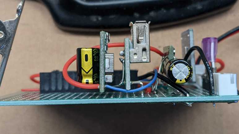
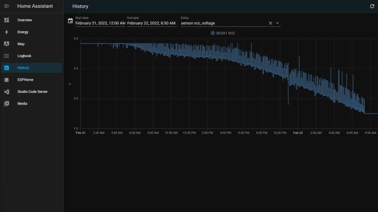
The ESPHome documentation for deep sleep described one way to prevent sleep using MQTT, keeping a node awake to receive firmware updates. But I wanted something even lower level hence the jumper and it became useful when I implemented the “low solar output, go to sleep” logic. Apparently INA219 component’s first power value always return zero. Which meant as soon as it booted up, that initial zero reading puts the node immediately back to sleep before it would even get on the network. (Never mind checking MQTT!) The solution is to switch from sampling values once a minute to sampling once a second, and make decisions based on average over a minute.

A different approach would be to go to sleep based on sun’s position in the sky, which can be queried and used in the Sun component. However, I expect this component has dependency on network connection (it needs to know the time, for starters) and would not be reliable if the network goes down. It also doesn’t know if the sun is obscured by clouds, so I think it’s better to use panel power output to decide what to do during the day. But I may explore using the Sun component in a future version to sleep all through the night instead of waking up every few minutes to fruitlessly check power level.

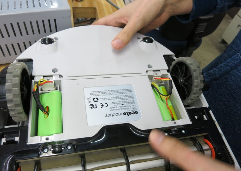
Strictly speaking, I don’t need to worry about stopping battery charging. I can supply 5V all day when panel delivers power, and trust the USB power bank charging circuit to keep the battery from being overcharged. But keeping lithium-ion cells full would shorten their useful life, so in the interest of battery longevity I’ll stop charging before full. On that topic: for optimal battery life I should charge it slowly over the course of the day, but I don’t have control over charging rate used by USB power bank.

One thing I don’t know yet is how the system will handle several rainy days in a row. I assume this panel can still generate enough power to charge an 18650 battery cell, but I might be wrong! I’ll have to wait for a long stretch of rain to come to Southern California, which may be a long wait. After seeing its behavior I can adjust for a future version.

Here’s version 1 of my ESPHome configuration YAML, and I expect to fine tune various hard-coded threshold values over the weeks ahead while I build more projects:

# Blue LED on the ESP8266 module signals connection status.
status_led:
  pin:
    number: 2
    inverted: true

# The goal is to charge once a day, and this flag tracks if we've already done it.
globals:
  - id: never_charged_today
    type: bool
    restore_value: no
    initial_value: "true"

# We can go to deep sleep to conserve battery, but sometimes we don't want to
# actually go to sleep. For example, when we need to upload a firmware update.
# Pin 13 is an input pin with internal pullup. It should be wired to a jumper
# that would ground the pin if jumper is present. Removing the jumper should
# disable going to deep sleep. To enforce this, call try_to_sleep script
# instead of calling deep_sleep.enter directly.
deep_sleep:
  id: deep_sleep_1

binary_sensor:
  - platform: gpio
    name: "Disable Sleep"
    id: sleep_jumper
    pin:
      number: 13
      mode:
        input: true
        pullup: true
    on_release:
      then:
        - logger.log: "Sleep jumper installed"
        - script.execute: try_to_sleep

script:
  - id: try_to_sleep
    then:
      if:
        condition:
          binary_sensor.is_on: sleep_jumper
        then:
          logger.log: "Sleep requested but staying awake due to override jumper"
        else:
          - logger.log: "Sleep requested and permitted by jumper"
          - delay: 5s # Allow sensor values to be sent.
          - deep_sleep.enter:
              id: deep_sleep_1
              sleep_duration: 10min

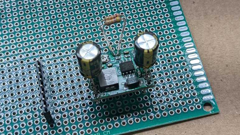
# This should be wired to a 1k resistor, which then connects to the enable pin
# of a power supply source. When ON, it should deliver power to charge the battery.
switch:
  - platform: gpio
    pin: D5
    id: charge_switch
    name: "Charge Battery"
    restore_mode: RESTORE_DEFAULT_OFF

# An I2C INA219 sensor monitors panel voltage, current, and calculates power.
i2c:
  sda: 4
  scl: 5

sensor:
  - platform: ina219
    address: 0x40
    shunt_resistance: 0.1 ohm
    max_voltage: 24.0V
    max_current: 3.2A
    update_interval: 1s
    current:
      name: "Panel Current"
      id: solar_panel_current
      accuracy_decimals: 5
      filters:
        sliding_window_moving_average:
          window_size: 90
          send_every: 60
          send_first_at: 15
    power:
      name: "Panel Power"
      id: solar_panel_power
      accuracy_decimals: 5
      filters:
        sliding_window_moving_average:
          window_size: 90
          send_every: 60
          send_first_at: 15
      on_value:
        then:
          # When power is low, put the board to sleep.
          # Note: upon boot, the first reading of current (and therefore power) always
          # seems to be zero, so we need to run moving average filters to ensure we
          # don't shut off immediately on power-up.
          if:
            condition:
              and:
                - sensor.in_range:
                    id: solar_panel_power
                    below: 0.01
                - sensor.in_range:
                    id: solar_panel_voltage
                    below: 3.0
            then:
              - logger.log: "Panel delivering low power, should go to sleep"
              - globals.set:
                  id: never_charged_today
                  value: "true"
              - script.execute: try_to_sleep
    bus_voltage:
      name: "Panel Voltage"
      id: solar_panel_voltage
      accuracy_decimals: 5
      filters:
        sliding_window_moving_average:
          window_size: 90
          send_every: 60
          send_first_at: 15
# ESP8266 ADC pin should be wired to a resistor just over 100kOhm to measure
# lithium-ion battery cell voltage. Values under calibrate_linear need to be
# customized for each board (and their resistors.)
  - platform: adc
    pin: A0
    name: "Battery Voltage"
    id: battery_voltage
    update_interval: 1s
    accuracy_decimals: 3
    filters:
      - calibrate_linear:
          - 0.84052 -> 3.492
          - 0.99707 -> 4.113
      - sliding_window_moving_average:
          window_size: 90
          send_every: 60
          send_first_at: 15
    on_value:
      then:
        - if:
            condition:
              and:
                - lambda: "return id(never_charged_today);"  
                - sensor.in_range:
                    id: solar_panel_power
                    above: 10
            then:
              - logger.log: "Panel has power, start charging for the day"
              - globals.set:
                  id: never_charged_today
                  value: "false"
              - switch.turn_on: charge_switch
        - if:
            condition:
              and:
                - switch.is_on: charge_switch
                - sensor.in_range:
                    id: solar_panel_power
                    below: 5
            then:
              - logger.log: "Charging paused due to low panel output"
              - globals.set:
                  id: never_charged_today
                  value: "true" # Resume charging if power returns
              - switch.turn_off: charge_switch
        # When battery is low enough to trigger this emergency measure, we
        # would not be able to activate charging ourselves. Charging needs to
        # be activated manually (or at least externally)
        - if:
            condition:
              sensor.in_range:
                id: battery_voltage
                below: 3.0
            then:
              - logger.log: "Battery critically low, should sleep to protect battery."
              - script.execute: try_to_sleep
    # We don't need a full charge to last through a day, so turn off charging
    # well before reaching maximum in order to improve battery longevity
    on_value_range:
      above: 4.0
      then:
        - logger.log: "Battery charge is sufficient"
        - switch.turn_off: charge_switch

Two Problems Controlling Buck Converter

My solar power monitor project runs on a ESP8266 microcontroller and an INA219 sensor powered by an old USB power bank. In order to charge it during the day from solar power, I’m trying out a new-to-me buck converter module because it exposed an “Enable” pin that was absent from my usual MP1584 buck converter module. I connected it (via a 1k resistor) to the closest available GPIO pin on my ESP8266 module, which happened to be GPIO0. Configuring ESPHome to use that pin as a switch, I could turn charging on or off from Home Assistant UI. I declared victory but it was premature.

I realized there was a problem when I put the ESP8266 to sleep and noticed charging resumed. This was a surprise. Probing the circuit I found my first problem: there is a pull-up resistor or a voltage divider on board my new buck converter module so that if its enable pin is left floating, it will activate itself as my usual MP1584 module would. This was mildly disappointing, because it meant I might have to unsolder a few resistors to get the behavior I originally wanted, and one of the reasons to buy this module was because I didn’t want to unsolder resisters from my MP1584 buck converter boards. As a short-term hack, I fought the existing circuit by adding a pull-down resistor external to the module. Experimentally it looks like a 10k resistor to ground was enough to do the trick, disabling the buck converter when enable input line is left floating.

But I wasn’t done yet, there’s a second problem to address: When ESP8266 was put back in the circuit, the charging would still resume when I put it into deep sleep. Probing the pin, I saw GPIO0 was at 3.3V while asleep. Reading online resources like this page on Random Nerd Tutorials, I learned the pin needs to be high for ESP8266 to boot. Presumably this means the Wemos D1 Mini module has a pull-up resistor on board for the boot process. Therefore I can’t use GPIO0 for charging control.

I went down the list of still-unused pins by distance to the buck converter on my circuit board. The next closest pin is GPIO2, which I can’t use as I’m already using the blue status LED. After that is GPIO14. It is usually used for SPI communication but I have no SPI peripherals for this project. Looking on the reference chart, it doesn’t seem to get pulled up or down while ESP8266 was asleep. After confirming that behavior with a voltmeter, I switched buck converter enable pin over to GPIO14. It allowed me to control charging from ESPHome and, when the ESP8266 is asleep, the buck converter stays disabled. Finally, the hardware is working as intended! Now I need to figure out the software.

Buck Converter Module with Enable Pin

After implementing over-discharge protection, attention turns to the charging portion of my project. For several of my projects over the past few years, I’ve been using a commodity buck converter module sold by many vendors. Built around a MP1584 chip (or a close-enough clone) they have worked quite well. But there were a few annoyances that made me want to try a different module.

  1. The first annoyance is that the commodity module is designed for variable output voltage adjusted via a tiny potentiometer. This gives great flexibility but it means every time I want to use a module I have to measure its output voltage on my voltmeter and adjust its potentiometer until I reached the voltage I wanted for a particular project. Most of the time I just want one of several common voltage values, usually 5V. It’d be nice to streamline that process.
  2. The next annoyance is that the MP1584 enable pin is not exposed on the module. There is an onboard voltage divider that automatically enables the chip whenever supply voltage rises above 3V. Usually this is what I want, but not always. And when I don’t want it, modifying the module is a hassle and prone to errors.
  3. And finally, the module’s connection pinout does not align with 0.1″ spacing, making its use on a perforated prototype board annoying. Recently I worked around this problem by adding capacitors to the input and output terminals then using those capacitor legs’ flexibility to compensate. But it would be nice if I don’t have to do that.

Looking over Amazon listings for “buck converter” I found an alternative candidate(*) advertised to address these annoyances. I bought a pack of twenty and it arrived in two bars of ten. We are to break off individual units like a candy bar. Some of the Amazon viewers complained, but I actually prefer this packaging over loosely packed individual modules. Here is the front and back of a single module:

The chip that runs the show is labeled AELH. This is different from Amazing listing pictures, which show a chip labeled AGCH. I found no information for either of those designations, so for the moment the exact identity of this buck converter chip is a mystery. For all I know, it might still be a MP1584 (or drop-in replacement) but that doesn’t matter right now. What matters is the rest of this module, which features an impressively compact layout.

Across the bottom we have four pins: VO+ (voltage output positive), GND (ground), IN+ (voltage input positive) and EN (enable). They have 0.1″ spacing, which I wanted for convenient prototype board/breadboard use.

There is a potentiometer in the top front corner, and six resistors below that. Looking on the backside we can see the potentiometer is connected but there are provisions for us to cut that trace and bridge one of the other pairs of pads to select one of the resistors that’ll give us a popular voltage, no fiddling with potentiometer required. I promptly cut the potentiometer trace and bridged the 5V pads with a bit of solder to see what I get.

I measured the output pins with my voltmeter, and it says 4.93V. This might be too low to avoid the dreaded lightning bolt icon used by a Raspberry Pi to signal low voltage, but should be good enough to charge a USB power bank.

Encouraged by this, I integrated this module into my solar monitor project. Where I found that the enable pin is almost — but not quite — what I had hoped for.


(*) Disclosure: As an Amazon Associate I earn from qualifying purchases.

ESP8266 ADC Helps Avoid Over-Discharging Battery

I took apart a USB power bank so I could bypass its problematic power output circuit and run a Wemos D1 Mini module directly on the single lithium-ion battery cell. But bypassing the output circuit also means losing its protection against battery over-discharge. This could permanently damage a lithium-ion battery cell, so it is something I have to reimplement.

I can to use the only ADC (analog-to-digital conversion) peripheral on an ESP8266 to monitor battery voltage. The ESP8266 ADC is limited to sensing voltage in the range of zero to one volt, so a voltage divider is necessary to bring the battery’s maximum voltage level of 4.2V down to 1V. The Wemos D1 Mini module has a voltage divider already on board, using 220kΩ and 100kΩ resistors to (almost) bring 3.3V down to 1V. To supplement this, I added another 100kΩ resistor between battery positive and Wemos D1 Mini analog input pin.

For an initial test, I connected the analog input pin to my bench power supply and started adjusting power. It did not quite work as expected, reaching maximum value at a little over 4.1 volts. I suspect one or more of the resistors involved have actual resistance values different than advertised, which is normal with cheap resistors of 15% tolerance.

As a result, I could not sense voltage above 4.1V, which is probably fine for the purpose of over-discharge protection. But I was willing to put in a little extra effort to sense the entire range, and added another 10kΩ resistor in series for a total of 110kΩ between battery positive and the Wemos D1 Mini analog pin. This was enough to compensate for resistor tolerance and allow me to distinguish voltage all the way up to 4.2V.

To translate this divided voltage back to original input voltage, I recorded values from two voltage levels. I recorded what the ESP8266 ADC reported for each, and what I measured with my voltmeter. These data points allow me to use ESPHome Sensor component’s calibrate_linear filter to obtain values good enough to watch for battery over-discharge.

Here are the relevant excerpts from my ESPHome configuration YAML:

  - platform: adc
    pin: A0
    name: "Battery Voltage"
    filters:
      - calibrate_linear:
          - 0.84052 -> 3.492
          - 0.99707 -> 4.113
    on_value:
      then:
        - if:
            condition:
              sensor.in_range:
                id: battery_voltage
                below: 3.0
            then:
              - logger.log: "Battery critically low"
              - deep_sleep.enter:

Ideally, I would never reach this point. I should make sure the battery is adequately charged each day. I will need to drop voltage output of solar panel (up to 24V) down to the 5V input voltage expected by an USB power bank’s lithium-ion battery charging circuit, and I want to try a new-to-me buck converter module for the task.

Running Wemos D1 Mini ESP8266 On Single Lithium-Ion 18650 Cell

I’ve taken apart a broken USB power bank and the 18650 battery cell within has stayed within nominal range. Its battery and charging circuit looks good, or at least doesn’t do anything obviously bad with that battery. I take it as confirmation of my hypothesis that it’s the 5V boost output circuit that is broken, which is great because I plan to ignore that part.

I couldn’t quite decipher the exact voltage regulator used on board the Wemos D1 Mini clone I bought via Amazon. But from my time running these modules on weak AAs, they seem to behave like LDO (low-dropout regulator) in that they are happy to deliver 3.3V even if the input voltage hovers barely above 3.3V. And if the supply voltage drops even further, that is passed through instead of quitting or making weird noises like as a MP1584 buck converter did. As long as I keep this 18650 cell operating in the healthy range of 3V to 4.2V, I can wire it directly to the “5V” input pin on a Wemos D1 Mini module and it should deliver enough power to run an ESP8266 and INA219.

To mount the USB power bank circuit, I first looked at the existing pin headers hoping they’ll mount directly on a perforated prototype board with 0.1″ pitch. Sadly they are slightly narrower than that (2mm pitch?) and would not fit. However, the battery connectors are close enough to 0.3″ apart that I could solder 0.1″ header pins and mount that to the board. This is a perfect way to tap directly into the battery.

I cut up a small piece of plastic (expired credit card) to serve as insulation between circuit boards and from there it was straightforward to mount this on my prototype board. The battery cell is then soldered to these pins and temporarily secured with tape.

I was all ready to solder these pins directly to the Wemos D1 Mini as well, but then I realized doing so would leave no graceful way to cut power. So I added a pair of jumpers (one for BT+, one for BT-) allowing me to turn things off if needed. Once I finished soldering (and probing to verify I hadn’t shorted anything) I put the jumpers in and saw the blinking LED of an ESP8266 starting up. Success!

Bypassing the broken power output portion of this USB power bank puts this little piece of equipment back to work instead of tossing it in electronic waste. But it also meant I lost over-discharge protection so I will have to implement that myself.

USB Power Bank Charging Looks OK

I just took apart an old broken USB power bank to see if I can use it as a power source for an ESP8266 project. I needed to get inside to see if the parts I wanted are working properly. Broadly speaking, a USB power bank can be divided into three major pieces of functionality:

  1. Battery cell itself.
  2. Charging circuit, which typically accepts 5V USB power and charges the battery cell.
  3. Power delivery circuit, which takes battery power and boosts it to 5V USB power for delivery.

This particular USB power bank works for little LED trinkets but would shut itself down whenever I plug in something more substantial. I appreciate that it would gracefully shut down instead of doing something spicy like burst into flames, but it is not terribly useful as a USB power bank that way. Each of its major pieces might have caused this behavior:

  1. Battery cell could have gone bad, so as soon as any load is placed on the cell the voltage immediately drops below the low-power cutoff point.
  2. Charging circuit could have gone bad, failing to properly charge the battery.
  3. Power delivery circuit could have gone bad and unable to deliver specified power.

I hope it is the power delivery circuit, which is unsuitable for microcontroller project power supply even when it is fully functional due to the following:

  1. Charge or discharge, not both. When a power bank is charging through its input port, they usually shut down their output port. This is fine for the designed usage pattern of USB power banks, but it is obviously not good if I want my system to keep running while it is charging.
  2. Auto-Off: When a power bank senses that their load has dropped below some threshold, they automatically shut down their output port. Again this is fine for charging power-hungry devices and shutting off when they’re full. But when I’m trying to keep my ESP8266 power consumption low, I trigger the automatic shutoff.

Given the possibility that the boost converter power delivery circuit (which I didn’t want anyway) is the broken part, I hacked this one open to see if the battery cell and the charging circuits are still good. The first check is easy: a volt meter confirmed this cell is within the 3V to 4.2V range for healthy lithium-ion cells. (Unlike some past project.) Then I used another USB power bank to charge this battery. My USB tester measured charging rate at 4.93V * 0.54A = 2.66W. When bucking this down to 3.7V nominal voltage this would work out to 0.72A. Rule of thumb for charging lithium-ion chemistry battery is to charge at a rate no more than “0.5C to 1C”. This cell has an advertised capacity of 2600mAh, so “0.5C to 1C” is the range of 1.3A-2.6A. Thus ~0.72A is comfortably under that range and should be a relaxing charge for the battery.

Charging rate: check!

The next test is whether the charging circuit would stop charging at the correct point, so I left it charging until it stopped. Shortly after it stopped, my voltmeter measured 4.16V across the battery terminals. This is less than the 4.2V absolute maximum for lithium-ion cells.

Charging halt: check!

With these tests, I have some confidence the battery cell still works, and the charging circuit correctly limits the charging rate and maximum voltage. Good enough for me to try putting them to work.

Battery Options for Solar Monitor

I finally got my solar power generation monitoring system up and running and I’m having a great time graphing data for visualization. But using weakened alkaline AA batteries I had available was only an interim solution, the next step is to make this into a longer running system.

This project is mildly annoying because I already have a large capacity battery system for capturing power from this solar panel. But I can’t run the panel monitor from the same battery because of different voltage planes: When charging, I measured a little over a volt of difference between input ground and output ground. As expected, there’s also a voltage difference between input positive and output positive. I don’t know the internal implementation of my battery charger, but it appears to be neither “common positive” nor “common ground” so I decided against adding any wires bridging those two sides.

Instead, I aim for an independent system that I can charge from solar panel while the sun is out and run my ESP8266+INA219 for the rest of the day. When the panel is not generating anything to monitor, I can put the ESP8266 into deep sleep. Successfully running this system on extremely weak alkaline AA batteries proved I don’t need a lot of energy storage capacity for this purpose.

On the old school nickel chemistry side of the battery world, I have nickel-cadmium (NiCad) battery cells I pulled from an old Dustbuster that could no longer run a handheld vacuum. I also have nickel-metal-hydride (NiMH) battery cells that could no longer run a Neato robot vacuum. While neither could run a big electric motor, they might still have enough remaining capacity to run a little solar monitor. I don’t have the means to charge them properly but that’s not really required anyway. Nickel chemistry batteries are fairly robust and many devices don’t bother with proper charging circuits as a cost saving measure, which was true for both the aforementioned Dustbuster and the Neato robot vacuum! So these batteries have already lived a hard life.

Alternatively, I could use a lithium chemistry battery. A proper charging circuit is very much mandatory for lithium chemistry batteries. While lightly overcharged nickel chemistry batteries would get warm as they dissipated excess energy as heat, overcharged lithium chemistry batteries aren’t as graceful and could burst into flames. (Which I guess is also technically “get warm to dissipate excess energy.”) Fortunately, since lithium chemistry batteries have become commodity consumer items, so have proper battery management circuits to accompany them. I can repurpose an old USB power bank for this job.

Plotting Solar Panel Voltage and Power

Ever since I bought a cheap solar panel array from Harbor Freight, I’ve wanted to quantify its output. Most solar power instruments were designed for house-sized (or larger) arrays, overkill for my little panel. I had instruments from the world of remote-control hobbies to measure voltage and current, but they were only instantaneous values displayed on screen. I wanted more! This motivated my journey evaluating software tools like InfluxDB database, Grafana visualizer, Home Assistant, and ESPHome. Plus building on what I knew about hardware components like ESP8266 microcontroller, MP1584 buck converter, and INA219 sensor. All with the goal of building my own solar production monitoring system.

I had thought I could make the ESP8266+INA219 sensor node run exclusively on solar power, but I gave up on that and have built a temporary setup powered by old tired alkaline AA batteries. Enough to give me a graph!

This was a fairly sunny day, so cloud cover effects were minimal. The solar panel was connected to a MPPT charger. I could see the power levels (green line) climb smoothly from sunrise, reach a maximum at noon, then smoothly fading off to sunset. This was mostly as expected. The power curve is not symmetric because there are a few things blocking sunlight from the east, reducing morning power.

While the power curve was mostly expected, the voltage levels were not. Until this graph I didn’t know solar panels would jump up so high on voltage before producing meaningful amount of power. (I don’t know if the MPPT charger makes a difference here.) If I had known this, I probably wouldn’t have bothered trying to make a solar powered circuit turn on and off based on voltage. Or if I did, I would have tried anyway and knew why it failed. From this graph I learned that if I am to draw upon solar power, I need to base my decision on power and not on voltage. But in order to read power levels, I need power for my INA219! There’s probably a clever way to circumvent this Catch-22 without batteries, but I’m going to take the easy way out and incorporate a rechargeable battery.

Running ESP8266 on Tired Alkaline AA Batteries

I retreated from trying to run a voltage & current sensor node exclusively on solar power. I’ll add some rechargeable batteries instead, but before I tackle the complexity of incorporating charging circuit (and charging logic) I took a side trip. I’m running the circuit on non-rechargeable alkaline AA batteries for a few days. And not even fresh batteries, these were already-weakened batteries from which I wanted to extract some more utility before I put them in a Joule thief LED circuit.

These batteries have open voltage of only around 1.1V, which is very low by standard of alkalines. (Fresh alkaline AAs measure over 1.5V.) And that open circuit voltage drops very quickly when I put it under strain of powering an ESP8266. So I keep usage brief, with sensor measurement and reporting run of just 30 seconds. (I later reduced it to 15 seconds.) Then I put the ESP8266 to sleep for five minutes. That five minutes give the chemistry inside these very weak batteries a chance to balance out and recover a little power before I hit them with another read+report session.

To measure how those batteries held up under the strain, I was going to wire up another voltage divider to the ESP8266 analog pin A0. But then I saw ESP8266 had an existing provision to report its chip input voltage VCC, no additional wiring necessary, and that capability is exposed in ESPHome. I chose this option out of laziness because it meant I didn’t have to warm up the soldering iron again.

The results: these weakened batteries could still give me a few days of readings before they started fading too much. I could see this in the Home Assistant log of reported VCC values.

For the first day or so, the batteries could deliver enough power that the ESP8266 didn’t see any drop in VCC voltage. But on the second or third day, voltage sags below 2.9V towards the end of my read+report session. This is visible as the lower bound of the VCC graph. During the five-minute sleep period, voltage recovers slightly and this is visible as the upper bound of the VCC graph. As the batteries continue to fade, both the upper bound (how much power the batteries could recover) and the lower bound (how low the voltage sags at the end of the session) decline over time. Eventually, VCC sagged to 1.75V and the ESP8266 could not run far enough to go back to sleep. That’s all I could get out of that particular batch of AAs. I’m happy they could run this circuit for a few days. They taught me some limits of running ESP8266 on low power, and gathered some interesting data along the way.

Start Simple with Alkaline AA Batteries

I thought I’d whip up a circuit to run exclusively on solar power. Growing around solar-powered electronics like desktop calculators, I knew it was a solved problem. But after running into obstacles, I have been humbled by the challenges involved and decided to fall back to battery power. A lot of solar power projects have a rechargeable battery somewhere in the mix, and I’m going to follow that precedence in the hopes of simplified energy management.

But as an intermediate stepping stone, I will adapt my circuit to run on batteries without worrying about the charging circuit just yet. I have the components I need on hand: a pile of alkaline AA batteries and a tray for 5*AA batteries in series.

A fresh AA alkaline battery has an open-circuit voltage just over 1.5V, and four of those in series would deliver more than 6V. Plenty for an ESP8266, but I’m not using fresh batteries for this project. My fresh AA batteries go into devices with motors or other high drain use. Once those devices complain the batteries were too weak, I move them into purely electronic devices with lower amperage demands. (TV remote controls, Hackaday badges, Xbox wireless controllers, etc.) When they are deemed too weak again, they go into my pile of AA batteries awaiting Joule thief LED duty. Open-circuit voltage for veteran batteries in this pile hover around 1.1V, thus I needed five of them in series instead of just four.

These 5-ish volts are too low to activate my modified MP1584 buck converter, which would no longer activate until input voltage of at least 13V. But that’s not a problem, because the Wemos D1 Mini clone board I’m using could run on 5V USB power. These batteries are pretty close to that voltage level, so I bypassed the MP1584 and connected the battery tray to existing “5V” pin on this module and used its onboard voltage regulator (which I didn’t trust to handle solar power directly) to deliver 3.3V to the ESP8266 and INA219. This worked pretty well.

Solar Startup Still Tricky

I have modified a second MP1584 buck converter module so that it would not activate until input voltage surpasses 13V, comfortably above the output voltage of 3.3V. I want to connect input pins to a solar panel so the associated components (ESP8266 WiFi microcontroller and INA219 voltage/current sensor) would be powered exclusively by the sun.

First is a test run with my bench power supply. Gradually increasing supply voltage starting from zero volts. Thanks to the modification, there were no odd behavior or sounds of a MP1584 trying to work with too low of an input voltage, which is great. As I increased voltage past the ~13V threshold, I saw the blue LED of my ESP8266 blink and it booted up as planned. This time, it was able to find INA219 on I2C bus, which is further than I got before.

Feeling optimistic, I connected this circuit to my solar panel at night and hoped I would wake up to find the system running. Sadly I woke up to disappointment, as there were no logged messages from the ESP8266. Probing the circuit with my volt meter, I confirmed a 3.3V supply voltage was present, but for whatever reason the ESP8266 failed to boot that morning. I manually disconnected and reconnected the circuit board, and this time ESP8266 booted up fine (now it has full daylight power) and started reporting values measured by INA219.

I don’t know what happened at sunrise. I hypothesize that when the solar panel output voltage rose past 13V, it has still yet to produce enough power to successfully start an ESP8266. So when MP1584 activated, it could supply 3.3V but not enough amperage to supply an ESP8266 through its boot process, putting it in a glitched state that was neither on nor off and stuck there until I power cycled the system. [UPDATE: Further experimentation found this hypothesis was correct, the panel would reach operating voltage well before generating appreciable power.]

I didn’t have my oscilloscope set up to capture the startup waveform to confirm or disprove this hypothesis. It’s clear there are additional subtleties I don’t know about starting up a circuit on solar power. Do I want to invest the time to learn and experiment with this problem domain? After thinking it over for a bit I decided “nah” and abandoned the idea of running everything exclusively on solar power. I’ll retreat to what I know and incorporate batteries into the system instead. Starting simple with household alkaline AA batteries.

MP1584 Modification Version 2

I’ve learned some lessons from the first round of modifying a MP1584 module for solar power input, and I thought I would try again. This time I started with a new module that hasn’t suffered the abuse of being enabled at too low of a voltage. To keep it that way, I still need to change the resistors on board so it activates at a higher voltage than the default 3V. Last time, I desoldered a surface-mount resistor, and it wasn’t a very neat job possibly damaging the board. This time I will go with a less invasive process and add more resistors in parallel with an existing resistor. This one between EN and GND was already on the edge of the board so it is easier to access.

I chose to add a 47kΩ and a 22kΩ through-hole resistor in parallel to the existing 100kΩ surface mount resistor between EN and GND. This should lower the effective resistance to 13kΩ between EN and GND. Combined with the existing 100kΩ resistor between EN and Vin, this should result in an activate voltage (EN ~=1.5V) somewhere around 13V.

A quick test with the bench power supply confirmed the new activation point. I then mounted it to a perforated prototype board using two 220uF capacitors as input and output pins. I didn’t put any effort into figuring out the perfect capacitance value, 220uF was just what I had available in a big bag of 100. (*)

Conveniently, using the capacitor’s legs to mount this board solves another problem I had with this type of MP1584 module: the input and output holes on the corners does not align with the 0.1″ spacing on a perforated prototype board or breadboard. But now that I have these capacitor legs, I could bend them to fit available spacing. Their length also leaves plenty of space for me to clamp on allegator clips. Useful for providing power from my bench power supply, and for measuring output with oscilloscope.

With a new candidate power supply in place, the next step is to solder the rest of the board to accommodate my ESP8266 and INA219 boards and test it out.


(*) Disclosure: As an Amazon Associate I earn from qualifying purchases.

Potential Explanations for MP1584 Behavior

I thought I could modify a MP1584 buck converter so that it would start up and shut down appropriately depending on whether its input voltage from a solar panel is enough to deliver 3.3V output. It destroyed my circuit instead and I could see what happened under an oscilloscope: when input voltage is close to the on/off transition point, output voltage is a sawtooth pattern with overshoot peak far above 3.3V. Why might this be happening? I can think of a few possible explanations:

  1. When replacing resistors for the voltage divider, I had damaged a part of the circuit critical to proper voltage feedback and regulation. I think this is very likely.
  2. Before I learned MP1584 enable voltage, I was giving it voltage that would trigger the default enable circuit (at 3V) which was lower than the target voltage (3.3V) and this damaged the chip. I think this is also fairly likely. Based on my reading of the MP1584 datasheet, it was not designed for variable-output adjustment with a potentiometer as is done on this board. There is an implicit assumption that the application engineer knows to make sure enable voltage is higher than target voltage and avoid this situation.
  3. On some boost converters, voltage overshoots are expected in low-load conditions. I regard this possibility as unlikely, since MP1584 datasheet was very proud at how it can automatically adjust to handle low loads. I found no mention of a minimum load required for proper operation.
  4. This is normal behavior for MP1584 close to enable on/off threshold. This is wrong for genuine MP1584, but if this chip was a knockoff (always a possibility when buying over internet from lowest bidder) then perhaps the knockoff chip has bad transitory behavior assuming few buyers would notice.

I don’t know which explanation is correct, and right now I’m not terribly interested in risking additional components to test these hypotheses. But I plan to do the following which should mitigate all of the above:

  1. Never use this specific modified module again.
  2. In the future, avoid enabling MP1584 when input voltage is lower than output voltage.
  3. The MP1584 module has a small surface-mount capacitor across both its input and output. For additional buffering, I will add larger capacitors to both sides for additional buffering.

Putting Modified MP1584 Under Oscilloscope

Something didn’t go according to plan with my latest project and destroyed a few components. The prime suspect is my recent modification to a MP1584 buck converter modules I bought on Amazon. By default, it would activate if input voltage is over 3V. This is far too low to deliver 3.3V output, so I modified it to defer activation until input voltage is nearly 12 Volts. A simple test with volt meter and simple LED was successful, but when I connected the ESP8266 microcontroller and INA219 sensor I released the magic smoke.

Before I connected those components I had checked the voltage output and it looked fine on a volt meter so I suspect there’s something with a transition behavior. This calls for an oscilloscope and I have a cheap DSO 138 that is better than nothing. Since the time I bought the kit and put it together, something has gone wrong with its voltage reference and now absolute voltage readings are unreliable. However, I think the relative shape of the waveform still resembled reality.

I first checked typical startup behavior: what does the 3.3V output look like when I connect this modified buck converter to 13V input? I set the oscilloscope to hold data upon rising edge trigger, and captured this:

The shape looks reasonable. It corresponds to graph in the MP1584 datasheet and shows the advertised soft-start capability to avoid a voltage overshoot on startup, which was my first suspect. I then turned the oscilloscope to continuous scan mode and adjusted my power supply voltage up and down. When I stay well above the input enable voltage of ~11.8V everything looks good, the buck converter maintained a steady 3.3V output. (It reads 5.27V on the display due to the voltage reference weirdness I spoke of.)

But things started looking dicey as I dropped close to 12V. I started seeing a sawtooth pattern to the output voltage. Instead of holding at 3.3V, I started seeing the voltage drop then jump upwards, with the magnitude growing wider and wider as I dropped input voltage. The worst was when I dropped into range below the 11.8V activation voltage, but still staying above the shutdown voltage…

Well, there’s your problem.

Without accurate voltage reference I don’t know exactly how many volts it whipped through, but at a guess it looks like it dips just below 2V before overshooting above 4V. This would definitely destroy components designed for 3.3V. It’s great that I see what is happening, now I need to think about why it happens and decide what I will do about it.

MP1584 Modification Did Not Go as Planned

I wanted a DC voltage/current monitor module to be powered by the same solar panel it is monitoring, which meant it shouldn’t start running until the panel started delivering enough power to run the circuit. I modified a MP1584 buck converter module so it would not activate until the voltage rises close to 12V. I wired this MP1584 module back into a monitoring circuit with an INA219 voltage/current sensor and ESP8266 WiFi microcontroller.

Before I powered it up, I used a meter to verify I hadn’t done anything silly like shorting Vcc to GND. This circuit also had a Vin+ and Vin- plus I2C communication lines SDA and SCL. I verified none of these were shorted to any of the others.

I then connected Vin+ and GND input pins to my bench power supply. I started with zero volts and slowly raised it until close to 12 volts, when I saw the blue led on my ESP8266 board blink signifying startup. I opened ESPHome dashboard so I could see the logged output from this ESP8266, and saw that it powered up and connected to WiFi successfully. However, it failed to find the INA219 as an I2C peripheral.

My first hypothesis was that I made a mistake soldering I2C signal wires SDA and SCL. I probed those connections and verified I hadn’t crossed those wires and there is electrical continuity. But ESP8266 still reported no response from an I2C scan.

The next hypothesis was that I used too thick gauge of wire for I2C signal lines and its higher capacitance had degraded I2C signal. I replaced the 22AWG wire with 30AWG wire, verified they had continuity and I hadn’t accidentally swapped SDA and SCL. But still no response on I2C scan.

While looking at the ESPHome YAML file looking for a configuration error, I smelled the distinctive scent of dying electronics. My first act upon turning back to the workbench was to turn off the power supply. Then I saw the INA219 was very obviously quite dead, a hole burned into the top and charred remains surrounding that hole.

I repeated the same basic probe I performed on this circuit before I powered it up, and this time my meter said Vcc is shorted to GND. Not good! I separated the components and measured them separately. The MP1584 power module did not short Vout (a.k.a. Vcc for the other two boards) to GND. The INA219 sensor module did, which is very likely related to why it died. And mysteriously, the ESP8266 microcontroller module reported the same… how the heck did it continue running with its Vcc shorted to GND?

Dumping both the INA219 sensor board and ESP8266 microcontroller board in my box of fried electronics, I took a closer look at my modified MP1584, suspected killer of electronics.

Raising MP1584 Enable Voltage by Replacing Resistor

I examined my MP1584 module and learned it was activating at far too low of a voltage. I want this buck converter to deliver 3.3V, and generally buck converters need input voltage a few volts (~2V) above the specified output. By that rule of thumb, my project shouldn’t activate until somewhere north of 5V, but it was activating at 3V and making a sound I could hear as it tried to perform an impossible task. This can’t be good.

I thought I would try modifying the board with different resistor values to raise its input enable voltage level. I will leave the low side resistor as-is at 100kΩ between EN and GND, and replace the high-side resistor. Looking through my commodity resistor pack, I thought a 220kΩ in series with 470kΩ should do the trick. Having 690kΩ between Vin and EN, and 100kΩ between EN and GND, should result in a voltage divider that activates EN (1.5V) when input voltage rises to approximately 11.85V.

At first, I thought I would have to switch to my small soldering iron tip to remove the existing high side resistor. But before I switched, I noticed my normal soldering tip is almost the same width as the resistor, allowing me to heat up both sides at the same time for removal. It left a big glop of solder doing so, but that wasn’t too hard to clean up. I then soldered the two resistors, in series, between the EN pad and Vin pad. Since these are through-hole resistors and not surface mount, it was not elegant. But it seems to work.

Slowly increasing input voltage with my bench power supply, I didn’t hear unhappy sounds at 3-5V. Nothing happened until I was close to 12V, at which point the MP1584 came alive and started delivering 3.3V. Success! Or so I had thought… and proven wrong by a puff of smoke.