Honda CD Spinner Demo

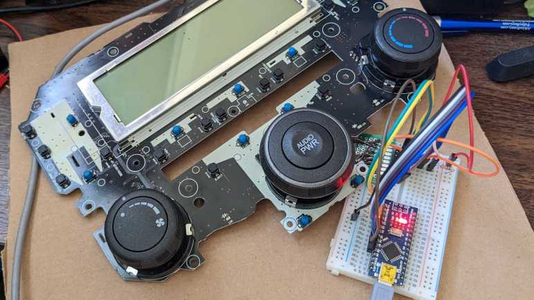
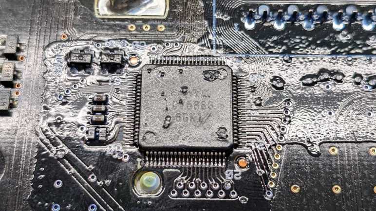
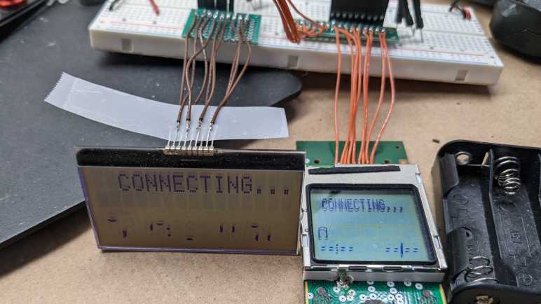
I am at a good stopping point for my exploration of a retired CD player control panel from a Honda Accord. At this point I can interact with all audio control button and knobs, and control what is displayed on its output LCD controlled by Sanyo LC75883 chip. My Arduino sketch toggles through several different modes when I press the “Mode” button (read via LC75883): Turn all segments on, or a “drawing mode” of turning on individual segments selected via the quadrature encoder knob. Very functional, but I wanted to put together something a little flashier before I move on to the next project.

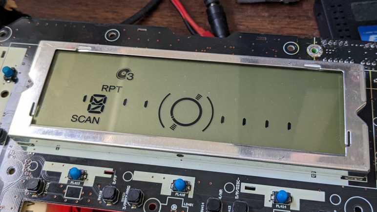
After I figured out the Toyota tape deck, I made a simple Larson scanner. I could do another Larson scanner with this LCD, but I thought I could put together something more interesting. The central attention-getting element of this segmented LCD is a series of 24 segments arranged in a circle. I’ve never seen this LCD work in normal operation, but since it is a CD player, I assume it showed graphics that resembled a spinning CD. A quick test confirmed that I could show a spinning animation, so I will make that the centerpiece for a demo. The next question is what to do with remaining segments.

There are ten 7+ segment displays. Four to the left of the spinner, three above, and four to the right. Some of these have additional segments, likely to display specific subsets of the alphabet. That works for static text, but it rules out scrolling text.

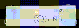
There are two additional segments that appear to be 7-segment numeric display but are not. Above the spinner is apparently a clock, as there are two elements that pretend to be “1” of a 7-segment numeric display but is in fact a single segment. And far to the right is a number that appear to be a 7-segment display but is in fact only three segments and thus extremely limited.

I also have a few miscellaneous elements for describing CD operation. “DISC”, “TRACK” “RPT”, etc. Plus six numbered CDs for the six-disc changer. I haven’t thought of anything useful to do with those beyond a Larson scanner-like animation.

I settled on the following:

  • Focus on center spinning CD animation using its 24 segments.
  • All the individually controllable 7-segment displays will use their outer 6 segments and also display a spinning animation.
  • There will be 12 frames in the animation, which works out evenly for the 24-segment CD and 6-segment outer digit segments.
  • Most of the remaining segments will form a near-vertical section of 1 in 12 bands, they will animate left-and-right in a Larson scanner-like manner.

The animation cycle: CD and digits spins clockwise, and the bands will move in one direction. The motion will slow, then reverse and acceleration. Then it will decelerate and reverse again, and the loop repeats. It didn’t turn out quite as visually interesting as I had hoped, but I’m not going to invest in the time to make a better animation. It is sufficient to show off the fact I have full control all segments independent of this LCD’s original designed purpose.

Source code for this demo is part of the investigation project available on GitHub.

Taking Stock of Honda CD Investigation Progress

When I was given a retired Honda Accord in-dash CD system, I thought its large LCD and tactile knobs might be interesting. After some introductory information and experiments with salvaged LCDs, I took this system out of my pile and started tinkering with it. Building on knowledge gained from earlier projects I was able to talk to this LCD’s Sanyo LC75883 driver chip and generate a segment map.

Segmented LCD units are customized for individual applications, so it was not a surprise to see this display was tailored for what a 6-disc CD changer needs to show. However, I was a little disappointed that seems to be all this LCD could show. This control panel also integrated HVAC control knobs for fan speed and temperature, so I had hoped to see some of that on the LCD. Doing so would have motivated the designer to make things a little more generic, like the alphanumeric text areas I saw on a cordless phone system’s LCD. Other reasons I had hoped to find a general-use text area are to show FM Radio Broadcast Data System or CD-Text information, sadly this system supported none of that.

When I tinkered with the Toyota tape deck faceplate LCD, figuring out how to read input was a nice side bonus. I had hoped to do the same with this panel. It had three knobs with good tactile feedback, and a lot of buttons. Tactile sensation or visual appearance for those buttons were nothing amazing, but they were real buttons on the board and not just copper traces that I’d have to bridge with something else. Sadly, I ran into strange problems trying to interact with the inputs on this circuit board that rendered things unusable.

The good news is that HVAC portions seems to be largely independent from the CD player functionality, which made it easier to figure out LCD and related controls. This is, unfortunately, also the bad news because the temperature and fan speed knobs are separate. I suspect they are handled by another chip on this board, which is also under a blue conformal coating and its surface markings unreadable. Perhaps it reads those knobs and drive HVAC motors directly from this board, as a nearby chip not hidden by conformal coating is a Toshiba TA8083F dual DC motor driver. I’m not inclined to figure out the motor control side of this board, but I’m still interested in those tactile knobs, so I’ll pull them off the board for a closer look.

Honda CD LCD Segment Map

I can talk to the LC75883 LCD driver chip on the faceplate of a Honda Accord CD/HVAC control panel, but I encountered problems using other peripherals. I don’t have the schematics for the circuit board and it would be a lot of work to generate one myself. At the moment I don’t have the motivation to undertake such a project. I have control of its LCD segments and I could generate a segment map for it:

Almost a quarter of the surface area on this LCD are allocated to CD icons 1 through 6, and many segments were consumed by the little circular graphic in the center. I guess that’s supposed to resemble a CD? We can control each pie slice to perform a rotating animation, but I was disappointed to learn the four dashes of each pie slice could not be controlled independently. So it is not possible to do a growing/shrinking circle animation, dashing my hopes of a polar coordinate VU meter. The clock up top is more or less as expected, but the four digits to the left and right of the circle are bizarre. Multiple different patterns that probably allows them to display certain letters in addition to numbers.

At least there weren’t too many segments that mislead us into think they were distinct segments. The most expected one was segment 9, which is actually both segments of the “1” and that makes sense for a clock that only needs to show 10, 11, and 12. Segment 60 includes both left and right brackets around the center, but I couldn’t think of many reasons why we’d want to control them separately anyway. The most bizarre is 134, which occupies 5 out of 7 segments of the right-most sub-sized digit. With it, that digit could only display 5, 6, 8, and 9. How is this useful? If I ever get a chance to play with the stock CD player of a 2007 Honda Accord, I want to see how this thing used to work. Right now, I ponder my next step.

Honda CD LCD Driver Problems

I’ve got the control panel for a Honda Accord’s CD/HVAC and I think I’ve found the electrical connections to talk to the LC75883 LCD driver. The software side was based on my LC75853 test program, which needed a few modifications to fit this LC75883 chip. It can control more segments, so I have to send three CCB messages of 9 bytes each instead of three messages of 7 bytes. Other than that, these two chips both respond to the same CCB addresses: 0x42 to send LCD control bits, 0x43 to read button presses. And they read the same number of buttons so there’s no change necessary there.

I launched the program and… nothing, the screen stayed blank while the Arduino ran. I turned the knob one step to see if my quadrature decoder routine worked, and I saw confirmation on the Arduino serial monitor but I also saw the screen came to life. What’s going on?

I quickly determined that the screen would go blank if one of the quadrature encoder phases are held to ground. The screen also blanks out if I press the button, which grounds a different pin. There’s something wrong with the electrical side, but it wasn’t as simple as a short circuit connecting +5V rail to ground. For one thing, the meter found no continuity between VDD and VSS. And for another, the +5V line stayed up when these events happen, allowing the Arduino serial output to continue running. I suspect I would learn more if I could see the behavior of the LCD partial voltage supplies VDD1 and VDD2 perhaps those voltages collapsed for some reason? But the chip pins were too small for me to get to them, and those pins weren’t brought out to the data connector for me to connect that way.

I can work around this grounding mystery by not pressing the power button and turning the knob two detents at a time. But even then, I have another problem: I could not read buttons with the LC75883 chip. Every time I pushed a button on the circuit board, the LC75883 signals that there’s a key activity to report. My code would go through all the motions to read the 32-bit report, but all bits would be zero. Could the “always low” data line be related to the knob/button grounding problem? Possibly, but at the moment I don’t know how to find it. I just worked around it the best I could to generate a segment map.


It’s not great, but my code to play with a LC75883 is on GitHub.

Preliminary Pinout for Honda CD

I have a Honda in-dash CD (and HVAC) control board and I want to see if I can make its LCD work. After I melted through conformal coating over the Sanyo LC75883 LCD driver chip, I was able to get an electrical connection with my meter so I can test for continuity between the pins (that are too fine for me to solder) to something I can more easily work with. I quickly found that much of the CD player functionality is connected to a small black rectangular connector I noticed earlier. Not just the LCD driver chip’s data communication lines, but also the big central rotary knob and button.

There is a large degree of uncertainty here, because I didn’t find what all of the pins did. I also found two pins that both appear to be ground, and I don’t know if there’s an important distinction between those two pins. This incomplete understanding explains the problems I will encounter later.

Using the numbers on the circuit board silkscreen, the pins are 1 to 24 from right to left. (Silkscreen shows 1 in the upper right, 2 in the lower right, 23 in the upper left, and 24 in the lower left.)

PinPreliminary NameDescription
7Vss (?)Either 7 or 9 is ground, maybe both?
9Vss (?)Either 7 or 9 is ground, maybe both?
14Vdd+5V power supply
16DOCCB Data Out
17DICCB Data In
18CLCCB Data Clock
20CECCB Chip Enable
21AEncoder A, connects to ground when knob is at certain positions.
22BEncoder B, connects to ground when knob is at certain positions.
24ButtonConnects to ground when “AUDIO PWR” button is pressed

Once these connections were made, I could make further progress. That is, running into an entirely different set of headaches.

Soldering Practice with Honda CD LCD Driver

Looking over the control circuit board for a Honda in-dash CD player, I saw an LCD driver chip which is a close cousin of one I worked with earlier in a Toyota tape deck. Even though I’ve never seen this CD control LCD run, and lacking the parts to reassemble the CD player, I think I have a chance to get it running just based on a datasheet and my recent experience. I do have a few obstacles I’d need to resolve first, though.

The first is that this section of the circuit board is coated in a conformal coating that prevents me from making electrical contact. It is also slightly sticky, which made it hard to work in this area. Every action adds debris stuck to this coating. Trying to wipe them off made things worse, as the coating grabbed fibers from my cleaning cloth.

I first tried isopropyl alcohol, which I understood to be the default cleaning solvent for electronics. I had hoped it would dissolve the blue coating but I saw no effect. I have a collection of household cleaning solvents harsher than isopropyl alcohol, but I don’t know which of them would damage electronics. Abandoning chemistry, I turned to heat: I put a small blob of solder on the tip of my soldering iron and touched it to the pins, hoping it will melt through the coating. The good news is that it did, the bad news is that it immediately heated the pins and existing solder and everything blended together into a bridge that connected all the pins I cared about plus many more that I did not. This was because of my second obstacle: these pins has very fine pitch. Datasheet says this SQFP80 package has 0.5mm pitch, which is far denser than the 0.1″ (~2.54mm) pitch I usually work with.

My attention was focused on the following pins:

  • 70: VDD +5V power supply
  • 73: VSS ground
  • 77: DO Data Out
  • 78: CE Chip Enable
  • 79: CL Clock
  • 80: DI Data In

And now I have a large solder blob that gave electrical continuity across all of them. Gah! Unpracticed at this scale, it took me over an hour to get the situation back into some semblance of control. Solder sucker took care of the major blobs, de-soldering braid took care of smaller portions, and a hot air gun melted off lingering whiskers. It was a disaster zone but I’ll be optimistic and call it practice. I still see signs of extraneous solder on the surface, and no guarantee there aren’t any hiding where I can’t see them. On top of that, all the heat to clean up the solder mess may have damaged the chip. Still, I had nothing to lose but time and everything to gain, so I proceeded.

I took the finest, smallest gauge wire I had on hand and soldered the first one to pin 80 DI (Data In.) And clearly this is not going to work: the wire is far too fat. But at least the conformal coating has been removed from these pins. So even if I can’t solder directly to these pins, I can use my meter to probe for another way to connect.

Honda CD Circuit Board

I have a circuit board assembly that appears to be the stock CD player and HVAC control board from a Honda Accord, integrated together instead of separate audio controls in DIN form factor. The front is dominated by a large LCD that I wanted to control as part of my current adventures into segmented LCD units. Unlike the Toyota tape deck, I don’t have the mainboard to get this up and running and probe its internal communication. Would I be able to talk to its built-in LCD driver, or would I have to control the LCD directly by generating my own voltages?

In addition to the large LCD, there were other elements of interest. This panel has three large knobs. The largest center knob is for audio control, the two side knobs are for air circulation fan speed (left) and temperature (right). All three knobs appear to use the same basic (if not identical) rotary encoders mounted to the circuit board, which is curious because they expose quite different user interfaces. The center knob has no end position and can rotate infinitely in either direction, which makes sense for a quadrature encoder. But the two side knobs each have their own distinct left and right endpoints and would need to know their absolute position. I would have expected them to be potentiometers instead of quadrature encoders, but at first glance all three appear identical. This will be interesting to look at later.

I was not surprised to find numerous green LEDs to indicate status of various settings. (LD6 and LD7 visible in above picture.) But I was surprised to discover the little blue background illumination lights (PL422 visible in picture above) were not blue LEDs.

They are actually tiny incandescent (filament) light bulbs underneath a blue cover. I guess this device was designed when blue LEDs were considered desirable but still expensive? If so, it’s pretty hilarious to see itty bitty light bulbs masquerading as blue LEDs.

All the buttons are surface-mounted units (SW7 visible in above picture) instead of the conductive wire trace type frequently seen in consumer electronics including the tape deck I took apart earlier. Small and compact, though their tactile feel is nothing spectacular.

Around the back, I see two electrical connectors. A large and sturdy green unit in the upper-left corner typical of automotive-grade connections, and a smaller black one just below and to the right of center.

This reminds me of the connector for the Toyota tape deck faceplate, but with 24 conductors instead of 16. Pins 1 and 2 are labeled on the right, and pins 23 and 24 are labeled on the left. Unlike the Toyota faceplate, none of the pins were labeled with their functionality.

A row of through-hole pins just above the central CD slot are consistent with all the common/segment pins for a segmented LCD array. These pins and its surrounding area are protected from the environment by a blue conformal coating that will make experimentation annoying. It’s a lot of bad news so far discouraging further exploration, until I followed LCD traces back to their control chip:

Barely readable through the conformal coating is “Sanyo LC75883”, which sounds very similar to the Sanyo LC75853 used on the Toyota tape deck faceplate. I found a datasheet for LC75883 and confirmed it is a sibling chip, speaking the same proprietary Sanyo CCB protocol. This is promising enough for me to try getting past that blue coating.

Next Segmented LCD Challenge: Honda CD

A quick review of my adventure so far: I have several segmented LCD units salvaged from various pieces of electronics. I’ve always thought “I’ll figure them out later” and finally decided to do it. The first one I got up and running was the simplest: a bare LCD with two digits of 7-segment numbers. Followed by a food thermometer LCD with many more number digits. Then I moved on to the realm of LCDs with associated driver chips controllers. I started with an old tape deck faceplate that I could examine while it was running and could find a datasheet. Then a cordless phone system that I could see running but didn’t have a datasheet. For the next challenge, I have an LCD that I’ve never seen running.

Browsing eBay listings, the shape and knobs of this thing matched the stock CD player for a 2007 Honda Accord. The temperature and fan speed knobs make it clear this was an integrated system combining the audio system and in-car HVAC. This type of integration has become more popular in recent model years, as car manufacturers moved away from ISO 7736 standard DIN form factor. I understand the visual appeal of a sound system cleanly integrated into a car’s interior design, but I’m not a fan of the fact upgrades become a huge hassle. For example, it is very popular now to have Android Auto and Apple CarPlay for connecting to our cell phones. It is a popular feature in modern cars’ integrated systems, and for old cars we can add such capability with standard DIN form factor aftermarket head ends. But for cars with non-DIN stock systems lacking Android Auto/Apple CarPlay, they are stuck in an awkward middle.

It’s not entirely impossible to upgrade them, it just takes more effort and money just to end up with something less elegant. An entire aftermarket ecosystem has sprung up to give DIN slots to cars that weren’t designed to have them. For several years I’ve been eyeing the Metra 99-7510HG(*) for my own 2004 Mazda RX-8. Perhaps the previous owner of this Honda Accord CD system thought the same and removed it in favor of a Metra 99-7803G(*) for DIN compatibility. Regardless of the reason, I now have this circuit board and I have nothing to lose by digging in.


(*) Disclosure: As an Amazon Associate I earn from qualifying purchases.

Pinout of LCD Salvaged From AT&T CL84209

When I retired my landline phone connection, I also retired my home phone. It was an AT&T CL84209 phone with built-in digital answering machine. I had a base station and though it supported multiple cordless handsets I had just a single handset. Without a landline, I took the entire system apart keeping a few parts for potential later use. Among the stuff I kept were two custom LCD units. One LCD was freed from the base station circuit board. I wanted to keep its backlight as well, but I accidentally destroyed it while trying to free it from the system. The other LCD was in the handset, and I kept it attached to its circuit board because I didn’t want to accidentally destroy another backlight.

They sat in my pile of salvaged parts for several years, until a few weeks ago when I took them out and started playing with them. I thought I could find some official documentation on these display units, but nothing came out of searches using every identifier I could find on these devices. Fortunately, thanks to the still-working handset circuit board and a logic analyzer, I figured out enough to control them from an ESP8266 Arduino program. This page is a summary of my findings.

Electrical

Both LCDs have nine hardware interface connections. Base station LCD uses pins, handset LCD shown above uses an FPC. I’ve numbered them 1 through 9 counting left to right as we are looking at the display. Despite the different physical form factor, electrically speaking they respond identically.

PinNameAdditional Notes
1EnableWe can make it always enabled by tying it high: use a 1kΩ pull-up resistor connected to pin 5 (+3.3V)
2SCLI2C clock logic level measured +3.3V, don’t know if it is +5V tolerant.
3SDAI2C data logic level measured +3.3V, don’t know if it is +5V tolerant.
4GroundRelative to pin 5
5VccSupply +3.3V to this pin.
0.82uF capacitor between this pin and pin 6 (Vboost)
6VboostOutput pin of built-in boost converter. Measured at +5.4V.
0.82uF capacitor between this pin and pin 5 (Vcc)
7VLCDHLCD segment voltage (high) 8kHz square wave from Vcc to Vboost
0.82uF capacitor between this pin and pin 8 (VLCDL)
8VLCDLLCD segment voltage (low) 8kHz square wave from 0V to Vcc
0.82uF capacitor between this pin and pin 7 (VLCDH)
9Voltage measured to match Vboost
Appears not connected to anything else on handset circuit board.

Digital

Both LCDs are I2C devices with an address of 0x3E. There are two types of messages:

  • Configuration set of 8 messages. Values were copied from logic analyzer capture and played back. Their exact meanings are unknown.
  • Data set of 3 messages. First message includes 15 bytes of alphanumeric data for the first line, second message for the second line, and the third message has 16 bits of digital data toggling state of custom LCD segments. (Which are different between LCDs.)

See the following pages for details:


Source code of software written to help with this investigation is publicly available on GitHub.

CL84209 Handset LCD Disassembly

I’ve mapped out the custom segments that occupy the lower half of this LCD, from the handset of an AT&T CL84209 cordless phone system. With that knowledge in hand, I wanted to dig a little more into this subassembly. When I removed it from the handset circuit board, I saw tantalizing hints of identification information that was mostly illegible through distorted plastic.

Four small sheet metal loops stamped in as part of the top metal shield held this assembly together. Once I popped those four loops freed of the tabs molded into the bottom-most piece of plastic, I could lay out all of its layers.

From left to right (bottom to top) we have:

  • Glossy injection-molded plastic bottom layer that is also most of the structural support.
  • Thin matte sheet of plastic.
  • Thicker (~1mm) clear sheet of plastic acting as conduit to distribute light from the single LED.
  • Thin frosted sheet of plastic acting as diffuser.
  • Glass LCD assembly with built-in I2C controller somewhere under the black blob.
  • Rubber surround (glued).
  • Topmost metal shield.

And now the objective of the exercise: a clear view of everything printed at the bottom of this handset LCD. Printed on a sticker is the following:

GWMS7728B
09470315313

Printed on the Flexible Printed Circuit (FPC) is:

7728-FPC-B-A152-4709

I see the logo of stylized “LCD” on both the FPC and etched into glass.

I saw the same logo on the base station LCD. And whereas that module was designated 6334, this one is clearly designated 7728 based on that number being repeated three times: etched into a layer of glass, on the white sticker, and also on the FPC connection.

This is a lot of additional information! Unfortunately, more information doesn’t guarantee success. Armed with this additional data, I still failed to find any details on this LCD module. But I’ll leave them here as a record hoping that my search skills will improve enough in the future to find something. But for today, I have to concede that I’ve tried everything I know. Lacking an official reference, I can only summarize all of my guesses about this device.

CL84209 Handset LCD Segment Map

Now that I’m properly driving this salvaged LCD, using its own voltage boost converter, I’ll map out its custom segments. The two lines of 15-character text uses the same character set as the LCD used in the base station of this AT&T CL84209 cordless phone system, but one space off from each other. On the lower half of the screen, this handset LCD has a different set of segments than the base station LCD. Fortunately, as they both respond to the same control protocol, I could use the same ESP8266 Arduino program to interactively select individual segments and write down which segment respond to which bits.

Comparing with the base station LCD segment map, there are some differences with obvious causes. For example, a battery gauge makes sense for the battery-powered handset. The battery outline segment (12) was an extremely informative element when I analyzed the digital control traffic, because it had been blinking on/off to signal low supply voltage and seeing that bit toggling on and off helped me zero in on the segment control bits. And now that I’m thinking about it, perhaps a blinking outline explains why 64 (outline around count of messages) and 100 (the actual “MSG#” text) are two separate segments. This was a design decision that puzzled me when looking at the base station LCD, but now I understand it gives the option of keeping “MSG#” on while the border blinks.

This handset LCD has a few additional custom segments, but two fewer 7-segment numeric digits. However, the hour tens digit of its clock area is thankfully a fully controllable 7-segment display, versus the base station LCD where all three horizontal lines were the same segment drastically limiting the digits it could display.

Numbering-wise, I see the “use 5 bits then skip 3” pattern. For example: 8, 9, 10, 11, 12 were used, then 13, 14, and 15 were skipped. I assume this has something to do with the segment/common convenience of wiring but couldn’t guess more without the chart like I had for Sanyo LC75853. Like the base station LCD, this handset LCD also skipped a byte entirely. Except in this case, it skipped the first byte (the first used bit was bit 8) instead of the final byte.

Putting together this segment map concludes the software side of exploring this LCD, I will now resume physical/mechanical exploration by taking apart this display assembly.


Source code for this investigation is publicly available on GitHub.

LCD Driver Has Own Voltage Boost Converter After All

I took apart an AT&T CL84209 cordless phone system and kept one of the handset’s circuit boards attached to its LCD unit. This allowed me to power up the circuit board and probe how its main processor controlled what’s shown on the LCD. I then took the LCD off of its board to take a closer look at the related circuitry.

Probing data indicated there was +5.2V on one of the LCD pins, and I had guessed it was supplied by a voltage boost converter somewhere else on the circuit board. I learned what they usually look like from the time I dug into the circuit board for a laptop screen, which included a boost converter to power its white LED backlight. On this handset circuit board, I see at least one assembly of an inductor next to a diode close to a capacitor, all the elements I now associated with a boost coverter.

But when I traced the phone handset circuit board, I didn’t find a +5.2V line going to the LCD. I found only a pair of capacitors. One of which connected the two square-wave generating pins (7 and 8) and another capacitor connected the +5.2V line to the +3.3V line. (Pins 5 and 6.) I don’t recognize what this arrangement does, but I could replicate it on my breadboard and see what happens.

The analog capture showed what happened: We now see pin 6 sit at 3.3V immediately upon initial power-up and rise up to +5.4V in response to the first I2C configuration message. Finally matching the pattern I saw on the original capture. This is amazing! The LCD driver chip only needs a +3.3V power supply and from that it generates its own +5.4V. There must be a built-in voltage boost converter with inductor and diode (or their functional equivalents) internal to work alongside an external capacitor. I thought I had learned enough about boost converters to recognize them when I see them, now I know I’m wrong. Earlier I had put a capacitor between the boost converter output line and ground, and that didn’t do what it did when I put the capacitor between boost output and +3.3V. I clearly have more to learn more about boost converters. But at least now I’m finally driving this LCD properly.

Unsoldering CL84209 Handset LCD

After mapping out the segments on the LCD salvaged from the base station of an AT&T CL84209 cordless phone system, I have reached the limits of what I can do in the absence of additional information. It has been wonderfully instructive to have a handset from the same system with its own LCD. I found that both LCD respond to the same command protocol, so I could power up the handset circuit and watch what happens under a logic analyzer then try to replicate the same behavior for the base station LCD. Now it is time for me to remove the LCD from the handset circuit board. I wanted to do so for two reasons:

  1. I don’t really want to keep the entire handset circuit board. It is designed to talk to a base station that no longer exists.
  2. It might be hiding some useful secrets underneath the LCD. I have a working knowledge of how all the pins work, but I might learn more from probing the circuit board independent of the LCD.

A bit of time with the solder station and I have separated the LCD to see that there’s… almost no components hidden underneath.

Just a single side-illumination LED in the upper right corner marked LED3. It feeds into a backlight mechanism much less sophisticated than a Fire tablet’s backlight.

But now we can see copper traces on this side of the circuit board. I was happy to see that my arbitrary left-to-right pin numbering matched what’s silkscreened here, purely by accident! I had thought pin 1 or 5 could be the power supply, and decided 1 was enable and 5 was supply. Now I get confirmation because 1 is a very narrow signal trace and 5 is a much thicker power trace. 2 and 3 were also thin digital signal lines for I2C, and 4 is connected to a big grid-patterned plane consistent with ground.

Those were great confirmations of my earlier guesses, but even better is information about the rest of the pins. The surprise was that pin 9 appears to be connected, because I had thought it was one of the capacitors I saw on the back side. Another surprise is that pin 6, which I thought would connect to a +5.2V supply, seems to connect only to one of four vias (marked by white circles) going to the other side of the circuit board.

Following those four vias to the other side, I find a pair of capacitors. Now that the LCD has been unsoldered, my multimeter could measure their capacitance: the one on the left read 823nF and the one on the right 775nF. Looking over popular capacitors on Digi-Key, these might be 0.82uF +/- 10% capacitors. But even more importantly: now that I can see the traces, I understand one capacitor bridges the +3.3V line and the +5.2V line, and the other bridges the two square wave lines. My electronics knowledge isn’t good enough to know what this means. But once I replicated this part of the circuit, I saw a voltage boost converter in action.

CL84209 Base Station LCD Segment Map

I have generated a printable lookup chart for the character set of an unknown LCD controller. This chip is embedded inside a black blob along the top edge of an LCD I salvaged from the base station of an AT&T CL84209 cordless phone system. The character set dictates what is rendered in two lines of 15-character alphanumeric text, each character is a dot matrix 5 pixels wide and 7 pixels tall. Below these two lines is a set of custom segmented LCD that can be controlled with 16 bytes, but there appear to be far fewer than 16*8 = 128 segments to control. A segment map will tell us which segments correspond to which bits.

I don’t have the datasheet for this chip, so I don’t know how it numbered its segments. I decided to mostly follow the precedence set by Sanyo LC75853 by numbering both bits and bytes in least-significant-first order. The difference for this map is that while LC75853 started counting from one, I’m going to start counting from zero.

My first attempt at mapping out these segments toggled them on/off alongside the character set data. When displaying characters starting with 0x00, I turned on all the segments whose number has zeroth bit set. For the character set starting with 0x10, I turned on all the segments with the next bit set, etc. In theory I could look at the on/off pattern as it cycled through 0x00 to 0x70 and determine its binary number. I also printed out the bit pattern to Arduino serial console, which looks like this:

0 1 10101010 10101010 10101010 10101010 10101010 10101010 10101010 10101010 10101010 10101010 10101010 10101010 10101010 10101010 10101010 10101010 
1 10 11001100 11001100 11001100 11001100 11001100 11001100 11001100 11001100 11001100 11001100 11001100 11001100 11001100 11001100 11001100 11001100 
2 100 11110000 11110000 11110000 11110000 11110000 11110000 11110000 11110000 11110000 11110000 11110000 11110000 11110000 11110000 11110000 11110000 
3 1000 0 11111111 0 11111111 0 11111111 0 11111111 0 11111111 0 11111111 0 11111111 0 11111111 
4 10000 0 0 11111111 11111111 0 0 11111111 11111111 0 0 11111111 11111111 0 0 11111111 11111111 
5 100000 0 0 0 0 11111111 11111111 11111111 11111111 0 0 0 0 11111111 11111111 11111111 11111111 
6 1000000 0 0 0 0 0 0 0 0 11111111 11111111 11111111 11111111 11111111 11111111 11111111 11111111 
7 10000000 0 0 0 0 0 0 0 0 0 0 0 0 0 0 0 0 

In theory this can work, in practice I quickly got tired flipping through images and decoding binary numbers by hand. That was a lot more work than having a quadrature encoder knob to interactively select segments to activate. I had avoided wiring in extra components out of laziness, but between manual binary decoding and soldering, I decided a bit of soldering was the easier path towards this segment map:

This map clearly showed this particular segment allocation used less than 5/8 of available segments. Starting from position zero, we would have five bits for five segments (0, 1, 2, 3, 4) then three bits that were unused. (5, 6, 7) Then five more segments (8, 9, 10, 11, 12) and three unused bits (13, 14, 15). This repeats until the final set of five (120, 121, 122, 123, 124) which were also unused.

I was surprised that segment 9 (“MSG#” title for message count) was a separate segment from 4, the rectangular border around message count. I had expected them to be a single segment.

I was also surprised and annoyed at segment 27, which lights up all three horizontal lines of the hour tens digit for the clock plus the lower left vertical segment. For a clock it made sense to restrict the tens digit to 1 or 2. But if so, why did they bother with segment 26 which isn’t useful for either of those digits? I had hoped maybe I could use it as a generic numeral display and not a clock, by leaving 65 and 66 (AM/PM) inactive. But segment 27 means I could only display 1, 2, 6, and 8. I have not yet thought of an interesting non-clock usage under those restrictions.

Obtaining a full segment map marks the end of investigating this base station LCD, I will now try to do the same for the handset LCD starting with its disassembly.


Source code for this investigation is publicly available on GitHub.

CL84209 Base Station LCD Character Set

After a look at the similarities and differences between two LCDs salvaged from an AT&T CL84209 cordless phone set, I was ready to start controlling one myself to get more data. Earlier probing indicated that I2C communication on the handset was 3.3V, so I’m going to use an ESP8266 because it is also a 3.3V part. The Arduino platform should be a good (enough) starting point, using its Wire library to recreate the I2C control messages I saw sent to the handset LCD.

After a quick test program to verify things worked as expected, I wanted to dump out the character set built inside this LCD controller. Since the character data is sent one byte per character, there are potentially 256 different characters in the font. Dealing with these powers-of-two numbers, I like to keep such information lined up with their hexadecimal values. The LCD can only print up to 15 characters per line, so I couldn’t print these in 16 characters batches. As a next best thing, I dropped down to 8 characters per line along with their starting hexadecimal value. A for() loop cycled through 16 such screens once per second, so I could see the entire character set cycle through.

This is one of the sixteen steps in the cycle. The first line shows characters from 0x70 to 0x77, and the second line from 0x78 to 0x7F. Using workbench lighting, I had trouble trying to photograph the screen without glare. So, I switched to backlighting the LCD using one of my salvaged LED backlights. I took a picture for each of the 16 sections with the intent to edit them together, but the slightly undersized backlight made it difficult. The center section of the screen is noticeably brighter than the edges, which makes it difficult to set a threshold to generate a nice monochrome reference chart. I had to consult Emily Velasco for some photo-editing tips. (I have now added “burn” & “dodge” to my photo editing toolbox.) After some very informative experimentation in GNU Image Manipulation Program I have a reference sheet suitable for printing. Using this chart, I could see that 0x7F is a solid block that activates all pixels of a 5×7 dot matrix, which I will use to as part of an “turn everything on” program to help map out its adjacent segmented region.


Source code for this investigation is publicly available on GitHub.

Handset LCD versus Base Station LCD (CL84209)

I have two LCD units salvaged from an AT&T CL84209 cordless phone system. One from the base station, and one still attached to a handset circuit board. The handset could still be powered up and ran, which helped me figure out how to interact with the base station LCD’s digital logic and analog voltage supply pins. Connecting them in parallel was a bad idea in many ways, but the risky experiment paid off telling me they both responded to the same I2C address and displayed similar but not identical things. Now that I have them side by side again, with some confidence I’m not damaging them while doing so, I have time to take a closer look at the similarities and differences.

Both of these LCDs have two lines of dot-matrix display on top, and a custom segmented LCD area below that. Each of the two lines consist of 15 characters, each character a dot matrix 5 pixels wide and 7 pixels tall. Its I2C control data indicates pixel-level control is not possible, since we only send a byte of data for each character. This is apparently tailored for alphanumeric information and not a full graphics display.

Curiously, given that both LCDs have two lines of 15 characters each, they seem to be one space off from each other when given identical control messages as they are here. For the base station LCD, we see two spaces in front of “CONNECTING…” and no space behind. In contrast, the handset LCD has that text centered on screen with one space in front and behind. If one of these screens had 15 characters and the other had 16, I could understand rendering one space off. But they both have 15 characters, so why would they do this?

The segmented area appears to be completely different between these two LCDs. Looking at the I2C traffic, 16 bytes were sent for 16*8 bits = up to 128 potential segments for control. Some of those bits go unused, as neither of these LCDs have 128 segments. For the handset LCD, I count 10 segments used for “–:– –/–” and an 11th for the battery icon. The same control bits just result in a nonsensical jumble of segments on the base station LCD, but I count 11 active segments in that jumble. It’s obvious they don’t have the same segments, but perhaps they use a similar subset that would be easiest to wire up in a LCD. I expect to get a better understanding once I start controlling this LCD with my own code.

LCD Behavior Between 5V Power Supply Candidates

There were nine pins on an LCD salvaged from an AT&T CL84209 cordless phone system. I found two candidates for its +5V power supply pin, but an experiment found that they both seemed to work. I doubt these are both +5V supply pins, as I expect the manufacturer would have removed unnecessary redundancy in the interest of cost. I hypothesize that one of them is the actual +5V supply pin, and the other one allowed +5V to leak through the circuit as an accidental side effect. Trying to guess which is which, I returned to recording analog behavior with my Saleae Logic 8.

For reference, here’s the behavior of handset LCD start-up that I want to replicate for pins 6-9. (Channels 4-7.)

The first experiment was to turn on the system without connecting any of the four mystery pins.

Channel 5 picked up 3.3V from elsewhere in the circuit. Channel 4 less so at 3V. The other two pins would sporadically spike up to one of those two voltages. This is definitely wrong, but I wanted to rule out the possibility this mystery LCD controller had a built-in voltage booster.

The next experiment was to put +5V (well, 4.8V) on Channel 4.

This looks much better. Channel 5 and 6 behavior looks correct, or at least close enough to my eyes. I don’t see anything that makes me think “Hmm, maybe this pin needs an external inductor, resistor, or capacitor.” Such as channel 7, who is trying and failing to hold 5V so I think it needs an external capacitor.

Then I switched +5V over to channel 7:

Channels 5 and 6 are again working roughly as expected, which explains why LCD segments look good no matter where +5V comes in. However, I see a weird multi-step behavior on channel 4 that is not ideal. Out of my options, I think I should put +5V on channel 4 and put a little capacitor (100nF ceramic) on channel 7:

Yeah, I think that’s my best approximation to the ideal behavior. The only difference I see is that, on the original data, channel 4 started with 3.3V then jumped up to 5V upon startup. It seems to be under LCD startup control, but I don’t see how. Maybe there’s something contributing elsewhere on the circuit board? I know there are still mysteries on this circuit buried underneath the handset LCD, something I intend to investigate later. For now, I hope putting +5V on pin 6 (channel 4) before initialization would not damage the LCD, because I plan on doing that for further exploration. Starting with a comparison between these two LCDs both responding to I2C 0x3E.

LCD in Parallel Test Round 2: 5V Power

There were nine pins on this LCD unit salvaged from an AT&T CL84209 cordless phone system. I think I’ve figured out five of them: 3.3V supply, ground, enable, I2C clock, and I2C data. The remaining four are still unknown but I noticed a correlation between their start-up behavior and the first control message sent to its I2C address of 0x3E. Perhaps those pins are not all input pins?

To get more data, I’m going to repeat the experiment of connecting two LCDs in parallel. One still mounted on remnant of a CL84209 handset circuit board, and the other was a bare module from the base station. The first time I tried this harebrained scheme, I connected all nine pins. Both displays ran, but at much lower contrast than usual.

This time, I won’t connect all the pins. Power supply, ground, and enable pins should be safe to connect in parallel. I2C data and clock lines are designed to connect to multiple devices in parallel, so electrically speaking it should be fine as well. But I2C is not designed to have two devices responding to the same address connected together. The protocol has no provision for such conflict resolution and usually I2C address conflict leads to chaos. The only reason we can get away with it this time is because these two screens respond identically (or close enough) so there aren’t conflicts to resolve.

With five out of nine pins connected in parallel, I will experiment to see what happens when I selectively connect the rest. For reference, here is the behavior recorded from the handset running standalone: Channels 4 and 7 should rise to 5V, channel 5 should be an 8kHz square wave between 3.3V and 5V, and channel 6 should be another 8kHz square wave from 0V to 3.3V in phase with channel 5.

Looking at this plot, I think I need to connect at least a pin to serve as a 5V power supply. Pin 6 (channel 4) and pin 9 (channel 7) are both candidates for 5V supply, since they both rise to 5V once things started up. Before the startup procedure, pin 6 (channel 4) received 3.3V as soon as the system received power, while pin 9 (channel 7) stayed at 0V until the startup procedure. Based on this difference, I think pin 6 (channel 4) is the better candidate to try, so I added a jumper wire to connect that to the handset circuit board.

It’s alive! And better yet, display contrast on both screens appears normal. Not faded-out as I saw in the previous parallel test with all nine pins connected.

Normal display contrast supports the hypothesis that the 8kHz voltage square waves were used for LCD segments, and furthermore this test implies those square waves were generated by the onboard controller. When these two LCDs were connected in parallel, their 8kHz voltage waves interfered with each other and lowered contrast on both. But if this is true, why do these signals need to be brought out as externally accessible pins? Why not just leave them internal? I don’t have a good guess for that.

As an additional data point, I disconnected pin 6 and connected pin 9. If my hypothesis is correct that pin 6 is the 5V power supply, disconnecting it and putting 5V on pin 9 should mean the display stays blank. Nope! My hypothesis was wrong or at least incomplete. When I disconnected pin 6, the display went blank as expected. But when I connected pin 9, the display came back to life. Both pin 6 and pin 9 could apparently serve as 5V power supply. Which one should I use? Perhaps taking another set of analog traces could provide some insight.

LCD Analog Activity Started By Digital Signal

I feel I have a working understanding of the I2C control messages necessary for controlling an LCD salvaged from an AT&T CL84209 landline phone system. But that is only part of the puzzle, because this LCD had input/output pins beyond I2C clock and data lines: there were four more pins to figure out. Represented by channel 4-7 in this logic analyzer trace:

Upon system power-up, one started at 3.3V and the others at 0V. Roughly two seconds after power-up, they come alive with two of them going up to 5.2V and the other two generating ~8kHz square waves. One between 0V and 3.3V, the other between 3.3V and 5.2V. I had assumed I would have to build circuitry to mimic these voltage values, but maybe I wouldn’t.

When zoomed in to when these pins became active, I could see the analog activity was immediately preceded by activity on the I2C bus. Comparing the timestamp against the list of decoded I2C messages, I found the I2C message visible on this graph is actually the very first set of messages sent to the LCD at address 0x3E.

This implies the LCD is not just a passive receiver of these signals, but an active participant who started something in response to the first initialization command sent over I2C bus. What we see here is some combination of functionality onboard the embedded chip, and some contribution from the circuit board. But I have no guesses at the division of labor between them. I assume the circuit board must contribute something to the process, otherwise the embedded controller could have just kept things internal and not incur the manufacturing cost of bringing those pins out.

I looked to the Sanyo LC75853N LCD controller datasheet I previously referenced for a different device to see if it had a counterpart to these pins. I note the OSC pin that required an external resistor and capacitor, and the VDD1 and VDD2 pins that required external voltage supply. None of these explanations fit the two pins that rose to 5.2V. The square wave between 0V and 3.3V might be an external oscillator, but I don’t know what that means for the other square wave between 3.3V and 5.2V.

On a quest for more data, I am going to try wiring these two LCDs in parallel again. The previous time was a risky experiment done in ignorance armed only with the fact I had very little to lose. This time I’m a little better informed which I hoped should translate to lower risk on the second try.

Examining Control Data for LCD at I2C Address 0x3E

My Saleae Logic 8 listening to the communication traffic on the I2C data bus of an AT&T CL84209 cordless phone headset heard thousands of messages within ten seconds of startup, addressed to ten different device addresses. I only cared about the messages related to its LCD screen and, fortunately, that data stood out and now I know this LCD is an I2C device with address of 0x3E.

Curious if knowing the I2C address will help me find more information on this LCD, I went online and… didn’t have much luck. Adafruit organizes a list of their I2C product addresses, but as of writing there’s nothing listed for 0x3E. I found the JHD1313 LCD module online, whose AiP31068 controller is an I2C device on address 0x3E. This chip is controlled with a series of command words, which is a control byte followed by a data byte. Different from the pattern I see on my Saleae decoded data, where character data is sent consecutively without command bytes in between. (Also, the datasheet annoyingly doesn’t give its I2C device address in hexadecimal or decimal form, only in binary form “011 1110” in the serial interface protocol chart.)

Empty-handed from this detour, I returned to my Python program parsing Saleae-decoded output. Out of 2569 captured messages, only 143 of them (5.57%) were addressed to 0x3E. This is a much more manageable number. Looking at that set, I found there were many two-byte messages and a few of the longer 18/19 byte messages.

The sequence of two-byte messages is almost identical throughout the capture, only difference is that the very first instance is one message shorter. (It omitted the final 0x00,0x02.) After that, the whole sequence repeats once every second. Lacking datasheet, I’m calling this the configuration sequence.

write to 0x3E ack data: 0x00 0x39 
write to 0x3E ack data: 0x00 0x1C 
write to 0x3E ack data: 0x00 0x70 
write to 0x3E ack data: 0x00 0x5F 
write to 0x3E ack data: 0x00 0x6C 
write to 0x3E ack data: 0x00 0x0C 
write to 0x3E ack data: 0x00 0x02 (Omitted from initial startup)

Shortly after this is sent, three lines of display data are sent. The capture included three variations. The first one is sent only once, immediately after the initial configuration sequence is sent:

write to 0x3E ack data: 0x80 0x81 0x40 0x20 0x20 0x20 0x20 0x20 0x20 0x20 0x20 0x20 0x20 0x20 0x20 0x20 0x20 0x20 
write to 0x3E ack data: 0x80 0xC1 0x40 0x20 0x20 0x20 0x20 0x20 0x20 0x20 0x20 0x20 0x20 0x20 0x20 0x20 0x20 0x20 
write to 0x3E ack data: 0x80 0x40 0x40 0x00 0x00 0x00 0x00 0x00 0x00 0x00 0x00 0x00 0x00 0x00 0x00 0x00 0x00 0x00 0x00 

The first two lines are all spaces, and the third line is all zeros. I interpret this as the “clear screen” for this LCD.

Afterwards, we have two variations of display data with “CONNECTING…” text. The first one:

write to 0x3E ack data: 0x80 0x81 0x40 0x20 0x43 0x4F 0x4E 0x4E 0x45 0x43 0x54 0x49 0x4E 0x47 0x2E 0x2E 0x2E 0x20 
write to 0x3E ack data: 0x80 0xC1 0x40 0x20 0x20 0x20 0x20 0x20 0x20 0x20 0x20 0x20 0x20 0x20 0x20 0x20 0x20 0x20 
write to 0x3E ack data: 0x80 0x40 0x40 0x00 0x00 0x10 0x02 0x01 0x04 0x00 0x10 0x00 0x04 0x01 0x00 0x02 0x10 0x04 0x00 

Differs from the second one by only a single bit in the third line, 0x00 vs. 0x10:

write to 0x3E ack data: 0x80 0x81 0x40 0x20 0x43 0x4F 0x4E 0x4E 0x45 0x43 0x54 0x49 0x4E 0x47 0x2E 0x2E 0x2E 0x20 
write to 0x3E ack data: 0x80 0xC1 0x40 0x20 0x20 0x20 0x20 0x20 0x20 0x20 0x20 0x20 0x20 0x20 0x20 0x20 0x20 0x20 
write to 0x3E ack data: 0x80 0x40 0x40 0x00 0x10 0x10 0x02 0x01 0x04 0x00 0x10 0x00 0x04 0x01 0x00 0x02 0x10 0x04 0x00 

This is consistent with handset LCD behavior blinking the “battery low” icon in the custom segmented LCD area. From here we can tell the first two lines are alphanumeric text, and the third line are bits for segmented LCD control where 0 is clear and 1 is active.

Looking at the screen, I see the battery icon blinking once a second. (Half second on, half second off.) Given this, I had expected to see the two variations of display data to alternate. Instead, it’s usually two of one style followed by one of the other. This mystery was solved once I looked at the timestamps: once every second, the configuration sequence is sent immediately followed by the current display state. Even if the display state hadn’t changed from the previous display update. In between these configuration sequences, the battery icon state is toggled every half second without sending the configuration sequence.

Thanks to Saleae Logic software and a bit of Python, I feel I’ve gained a working grasp of digital control communication for this LCD. I don’t know what any of those control flags individually mean, but I wouldn’t need to fully understand them if I just wanted to send alphanumeric data and toggle segments. Outside of these digital signal pins, there’s still the unknown of analog voltage pins. But looking at the timeline, I noticed an interesting correlation.