Chunghwa CLAA133UA01 Circuit Board and LED Backlight

I tried and failed to salvage the polarizer film of a Chunghwa CLAA133UA01 display panel, but that wasn’t the primary objective anyway. I turned to the real goal of salvaging its LED backlight and the first step is to remove the perimeter protective film. Most of my prior salvaged panels were held together with thin black plastic tape, this panel is slightly different in its use of shiny metallic foil tape. I was surprised to see it, as I thought foil would short-circuit the components underneath. Perhaps it is some sort of metallized plastic instead of metal foil. This stuff rips more easily than others but at least its adhesive still came off cleanly.

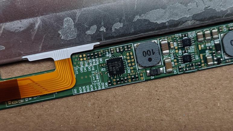
Once the foil was removed, I could see three important-looking chips on the circuit board.

Closest to the cable connector is a chip marked MST7337F-A AQ2T842B 1049B. A web search found Kynix Semiconductor MST7337 which is a chip for NTSC/PAL/SECAM automotive TV applications. I don’t think this is the right chip, but the correct answer eludes me. I might have better luck if I knew the logo, which is distinctive but not one I recognize. I didn’t see that logo on the Kynix Semiconductor page.

The next chip was marked AAT11771 A2U274 1052. A web search found a hit: Advanced Analog Technology AAT11771 is a controller for driving TFT LCD displays.

The third important-looking chip was marked A706B A38T 66040. Its proximity to the LED backlight connector makes it a prime candidate for the LED driver, it’s even next to the inductor + capacitor pairing consistent with a boost converter to raise voltage high enough to drive strings of LEDs. A search for A706B found that A706 is a standardized grade of steel bars for concrete reinforcement, but I saw nothing about a LED driver chip.

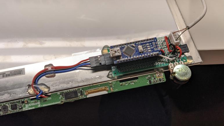
Pulling up the backlight connector for a look, I can see there are five thin conductors, one per contact point plus one thick conductor using three contact points. Remaining contact points between them are apparently unused. Based on what I’ve seen on other panels, I guessed the thick conductor is a common source for five current sinks for five parallel strings of LEDs.

This hypothesis was quickly and easily tested with a LED tester, so if I never manage to find information on that LED driver chip I should at least be able to drive these strings directly via copious test points visible in that area of the circuit board.

Until I find need for another diffused LED light source, this is a good stopping point. I put the LED backlight back into storage and pulled a non-dead panel out of my hardware archives. This one is still attached to a nominally working HP Stream 7 tablet.

Chunghwa CLAA133UA01 Polarizer Glue Stronger Than Polarizer Film

After verifying I could illuminate LED strings of a LG LPP133WH2(TL)(M2) salvaged from a Dell laptop, I set it aside to work on the final panel in my stack of LCD laptop panels. This was salvaged from a Sony VAIO laptop whose model number I no longer know.

The original owner had spilled some cola on it. Good news: the spill did not immediately kill the machine so data could be pulled off averting any loss of data. Bad news: the computer started failing intermittently in strange ways as corrosion took hold, and eventually died a few weeks after the initial spill.

Removing the panel I see a label with designation Chunghwa CLAA133UA01. (Along with some dried coke residue.) Web lookup indicated this is a LED-backlit panel with 1600×900 resolution. Better than the 1366×768 resolution we see on baseline laptops today, but still short of full 1920×1080 resolution. Like the rest of my stack of panels, I decided it was not interesting enough to revive as a display.

My first task was removing the polarizer film in the front of the display, something I have yet to perfect through several past experiments. So far I’ve been able to remove the film in one piece but failed to clean off adhesive residue. For this panel, I didn’t even get that far. This panel used glue that was very strong, apparently stronger than the tensile strength of the polarizer film! Roughly a quarter of the way through peeling, the film tore apart and I decided to abandon polarizer retrieval.

Looking at the tear was mildly interesting. It was a zig-zag pattern instead of a straight line. This material is weakest at plus or minus 45 degrees relative to screen viewing orientation. Does that have any relation to polarization angle, or is it indicative of something else? I don’t have any tools to probe that question so I will set it aside for now and move on to the LED backlight.

LED Backlight of LG LP133WH2 (TL)(M2) Laptop LCD Panel

I’m pulling apart some retired laptop LCD panels. For the latest panel, I decided to work on the polarizer film first and I was encouraged by those results. I’ll probably try the polarizer first for future panels. But before I move on to the next panel, I want to get a closer look at the LED backlight from this panel I pulled from a retired Dell laptop. The label says it is a LG Display LP133WH2 (TL)(M2) module. A quick internet search says its pixel resolution is 1366×768, which is pretty low by today’s standards and not worth the effort to bring back online as a computer display.

Like many previous modules, it had tape all around. Unlike some previous modules, there are several different types of tape involved.

Peeling back the tape, I could see the backlight connector in the center. The previous few panels had them to the side. I’m not sure what design tradeoffs are involved in the different placements.

The chip footprint closest to the backlight connector is unpopulated. This is usually a sign there’s another version of the device with enhanced features, but I’m not sure how that works for a display module like this. Whatever it may be, the absent chip is certainly not the backlight LED controller.

The other chip on this side of the circuit board is labeled LG SW0641A. I’m amused that my not-helpful search results included a LG clothes washer with that model number. I’m not sure what this is, but it is definitely not a clothes washer. It is probably the main display controller that talks to the rest of the laptop.

Flipping the panel over, high density data connectors for the LCD array are visible as well as two chips.

Searching for information on a SiW SW5024, I came across vendors willing to sell them but not much else.

But that doesn’t matter, because a search for ADD 5201 written on the other chip resulted in a pointer to a “High Efficiency, Eight-String White LED Driver for LCD Backlight Applications” by Analog Devices. Jackpot!

While the chip can drive up to eight strings, it appears we only have four on this panel. I see a VOUT_LED test point that fans out to four conductors on this connector. And I also see test points corresponding to four strings. FB1 is to the left, below VOUT_LED. FB2, FB3, and FB4 are to the right. If it follows convention of other panels, VOUT_LED would be the current source and FB1 through FB4 are sinks for each of four parallel strings of LEDs.

Probing those points with a LED tester confirmed the hypothesis, and highlighted another difference on this panel. Previous panels with parallel strings of LEDs would interleave them across the bottom. With an interleaved design a single failed string would still leave most of the display illuminated. But in this panel, each of these four strings are assigned a quarter of the panel area. So if one string failed, one quarter of the display would be darkened and difficult to read. My guess is this method is easier (and cheaper) to wire as a tradeoff for fault tolerance.

With the LED strings verified to illuminate, I set this aside and started working on the final disembodied laptop display panels currently in my possession: a Chunghwa CLAA133UA01 from a Sony VAIO laptop.

Start with Polarizer Film Transfer

I’ve been interested in salvaging the polarizer film from a LCD panel but I’ve had problems removing the glue without destroying the film. I had the idea to leave the glue in place but transfer it to something else that is clear, like a sheet of acrylic. I wouldn’t call my first experiment a success, but it was encouraging enough for me to start with the film for my next salvaged laptop LCD panel.

There were two advantage I hoped to gain by pulling that sheet while the LCD module is still intact. First is physical strength, as the glass still has all of its reinforcements and I hope it will be less likely to break as I pull on the polarizer film. Second is thermal inertia, I’ve learned that a thin sheet of glass cools too quickly. By leaving the module intact I hoped it would stay hot longer.

The next LCD panel was salvaged from a Dell laptop whose model number I no longer remember. (Possibly a Vostro 3350?) It had a lovely bronze surface finish so I also kept the mounting frame for this panel.

Just like before, I left it out in the Southern California summer sun to soften the glue.

A razor blade got me started in a corner.

A ruler was used to give me a flat edge to hold against the glass, which along with keeping the module intact meant I didn’t break this LCD glass during polarizer film removal.

And just my luck, the glue for this particular sheet isn’t particularly tenacious and didn’t want to stick to the acrylic. And where it did stick, it wasn’t as optically clear as previous films.

A little bit of mineral spirits helped the glue settle against the acrylic. Still not optically clear, but I’m pleased with my progress on reducing surface imperfections.

Polarizer Film Transfer Experiment

I’ve got a collection of old LCD panels that I want to turn into LED lights by salvaging their backlight. In the course of doing so, I also get some auxiliary pieces like a rigid metal frame. Another common piece that I’ve been working to salvage is the polarizer film. A sheet of polarizer film is a part of every LCD panel, interacting with the liquid crystals within to block or allow light as needed to create the picture on screen. Because it is directly on the optical path, it’s important for it to be held against the screen in a way that minimizes optical distortion.

In practice this means a very thin layer of very tough clear glue that keeps the film flat against the glass. I’ve been struggling with how to best salvage the polarizer film. While I could peel it off the glass, that leaves a layer of glue that I have yet to figure out how to remove. I worked my way from isopropyl alcohol to mineral spirits up to acetone. I found that acetone would dissolve these glues very well, but using enough to dissolve the glue also damages the film. I have yet to successfully clean off a sheet of polarizer film.

As an experiment, I want to see if I can sidestep the problem of removing the glue. Instead of trying to clean it off, keep the glue and instead transfer the polarizer film along with its glue onto something more durable and clear than the glass layers of a LCD panel. I decided to start with a sheet of acrylic I had bought for laser cutting. The pandemic cut me off from the laser cutter I had planned to use with it, so it is now fair game for use in this project.

As I did before, I left the LCD assembly in the hot Southern California summer sun to soften the glue. It didn’t take much heating, two thin layers of glass and a sheet of plastic film had very little thermal inertia. So little, in fact, that the glue solidified and cooled within a few minutes after being taken into the shade. This is disappointing, because it meant I need to move back outdoors and perform this work under the sun.

I’m still learning to work with such fragile sheets of glass, so it wasn’t a surprise when I cracked it (further) making this polarizer film project difficult. Annoying, but not a surprise.

Thankfully a LCD panel had multiple edges, so rather than give up I turned the panel 180 degrees and started peeling the other side for practice.

I was able to peel the remainder without further cracking glass, and transferred to my acrylic sheet for a quick test.

There are a lot of air bubbles in there so the result is pretty bad, but there are portions where the glue happily sucked back down to the sheet of acrylic leaving an optically clear path. If I can figure out how to increase the percentage of area that shows this clear path, I think this approach can work. This particular example, however, is pretty screwed. Any attempt to make that adhere optically clear will be continually foiled by tiny bits of broken glass.

But even though I think it’s doomed to failure, I see a learning and practicing opportunity before me so I pulled out a razor blade and started trying to remove the broken glass pieces. This is a terrible idea. I’m dealing using a sharp piece of steel to deal with with sharp pieces of glass. Not only does the blade scratch and damage the film surface, it can’t get all the little glass pieces. I have not set myself up for success with this test, but at least I managed to avoid cutting myself open in this exercise.

The results were completely unusable. That said, it actually turned out far better than I had expected. In this picture the glass shards I had removed are sitting on the keyboard beyond the polarizer film and acrylic sheet. They are several centimeters away and there’s enough clarity for us to see them. I think there is promise in this transfer approach and I intend to practice it on the next few panel salvage projects. In fact, the very next panel salvage started with the polarizer.

Amazon Fire SR043KL Display Disassembly

I have taken apart an Amazon Fire tablet (SR043KL) and retrieved the prize I sought: an intact display assembly under the cracked digitizer glass. Though presence or absence of cracks in the LCD wouldn’t have mattered for my project anyway. My objective is actually the backlight behind it.

Just like the LG laptop display I disassembled earlier, this display module is held on all edges by thin precision black tape. Peeling back the tape, I had hoped to find a LED backlight driver as I did on the laptop display, but not this time. There are a few small passive components here, but the backlight driver must be on the mainboard hidden under one of those metal shields.

Lacking an easily accessible LED driver, the next objective is to hunt for the backlight LED circuit itself. I expected them to be the largest traces relative to the other components, and I see two exposed contacts already labelled with + and -. Hmm… could it be that easy? I could do a quick test: since these two points were already exposed, soldering some wires to them were straightforward.

In order to see if the LEDs glow, I peeled back more of the tape. Slowly increasing the voltage, I started seeing a glow at around 15V. Wow, it’s really was that easy.

I have no idea how to drive this LCD array, and I have no intention to learn. My objective for today is the LED backlight. So after I peeled away all black tape around the perimeter, I sliced the high density LCD pixel data ribbon in order to separate the two parts.

There isn’t much more to be said about the LCD array. I was able to peel off the polarizer film, this time without cracking any glass, but using acetone to clean off the adhesive once again caused the film to disintegrate. That’s two strikes against acetone, I’ll have to try something else next time.

I have to put more thought into polarizer film recovery, but that’s only a mild distraction from my fascination with the backlight and its sheets of optical magic.

Laptop Backlight Is Now Webcam Light

I have successfully salvaged the backlight module of a LG LP133WF2(SP)(A1) laptop LCD display, which meant in addition to all the lessons I learned along the way, I now have a rectangular ~15″ diagonal LED panel that can emit diffuse white light. What do I do with this light? I looked around at places in my life where I felt I had a lighting challenge, and the most relevant issue in these pandemic times is my webcam for video calls.

Right now my primary workstation is in a room with decent sunshine during the day but only a dim overhead light at night. Resulting in grainy video as the camera struggles to capture limited light, and the position of the light also cast some unfortunate shadows. There is a far stronger light in the room, but it is set up to illuminate my workbench behind me. If I forget to turn that light off during a video call, I can immediately tell there’s a problem because I turn into a silhouette on camera. What I need is a light behind the webcam, which is something I can easily buy. There’s an entire product category for this usually in the form of a ring that surrounds the camera. What I have on hand is a rectangle and not a ring but I still want to try it. To test this idea I’ll need a way to mount the panel on top of my computer monitor.

Since this is supposed to be a quick test, I didn’t want to go full out with CAD and 3D printing. I pulled some cardboard boxes out of the paper recycle bin and happily started cutting with my Canary cutter. It was a highly iterative trial and error process and after a few hours I had a cardboard contraption that held the panel above my monitor, sitting on its top edge.

This top edge mechanism was the trickiest part of the design as it needed to be strong enough to hold the weight of the entire assembly. This assembly was heavier than I had originally planned because I didn’t foresee the very obvious fact the panel would make the assembly top heavy unless I added a counterweight (in the form of a large lithium polymer battery pack) sitting below the lip in order to drop the center of gravity. This is too much weight for just cardboard to hold against, so I had to pull in some plastic to help. But still no 3D printing: I cut up an used-up Starbucks gift card into an inverted U shape to give me the necessary strength at this key junction on top of the monitor.

This is definitely not the final design. I want to move the panel lower and further away from my face so it is directly behind the camera instead of above it. I chose the current panel height because I needed to be able to reach the brightness adjustment knob mounted in the lower left. After I put this box together, I realized I could have easily rotated the panel 180 degrees so the knob is in the top right corner instead of the lower left, allowing me to sink the bottom edge below the camera. Alternatively, I could have the brightness PWM adjustment module as an external module mounted elsewhere.

So that is the first and most significant change I want to make for the next iteration, but I’ll use this cardboard first draft for a little while longer and see what other issues I might want to address. In the meantime I proceed to the next backlight exercise with an Amazon Fire tablet.

Installing Arduino Circuit, Round 2

I have a small circuit board to generate a PWM signal that tells the TPS61187 LED driver chip how bright to illuminate the LED of a backlight I salvaged from a cracked LG laptop LCD screen model LP133WF2(SP)(A1). It’s not the most compact thing I could have built, but it was simple and quick. Or at least it was supposed to be quick, because my first attempt at installing it destroyed a solder connection to the screen control board and I had to redo my soldering joints and secure them with hot glue in the hopes I wouldn’t destroy any more solder connections.

Now I’m installing the circuit board again, and I realized I forgot a very important detail: The location I wanted to mount this thing is on the metal frame of this backlight, because I didn’t want to block any light that might emit from the plastic back side of the panel. My circuit board had many soldered connections on the bottom. Putting soldered connections on a metal plate causes short circuits! Fortunately I realized this before destroying anything.

Adding to the bulk of this project, I placed a sheet of clear plastic packing tape as the first layer of insulation, followed by two layers of double-sided foam tape to raise it off the first layer. The foam tape wasn’t as secure as I had hoped, so I warmed up the hot glue gun again to squirt out some secure standoffs. Thanks to the first layer of clear packing tape, I’m semi-confident I can replace this with a different PWM generator if I decide to do so in the future. But for the moment I have completed all electrical work for this light panel that I can power off USB. A happy end result of a lot of very useful and valuable electronics lessons learned building this project. From reading datasheets and their schematics to figuring out what to do when things go wrong.

But the happy result does have one downside. When I have a failure, I can dispose of the pieces after thanking them for their valuable lessons. But when I have a success, I can’t just throw it out! So now I have a ~15″ diagonal rectangular LED light and I need to think of something useful to do with it.

Need Backup Plan For TPS61187 Interface

I had thought I was near the finish line for my backlight revival project, but then I tugged on one wire a little bit too hard and destroyed the circuit board test point I had soldered to.

This is bad, and it got worse. As I tried to gently unwind this LED_EN wire, it was not gentle enough and the soldered points for Vin and GND started unraveling as well. For those two wires I had soldered to either end of a (relatively) large surface mount decoupling capacitor bridging those two voltage planes, because the tops of these capacitors presented a metallic surface area for me to solder to. I had thought they were metal end pieces, but they were actually a thin layer of metal that I just learned would peel under stress. The good news was that I was able to melt the solder and remove those wires before they did any permanent damage, the bad news is that I’ll need another approach for these connections as well.

Since I’ve already proved to be clumsy with three out of four wires, I pulled out my hot glue gun to better secure my solder points starting with my PWM wire that still remains. I dropped a dollop of hot glue and, as I pulled my hot glue gun away, I felt the now-dreaded “pop” sensation in my fingertip holding the wire in place. I think I just lifted the PWM copper pad, too! Fortunately, my meter said I still had electrical continuity. So even if I did lift the pad, it is still connected, held in position by my drop of hot glue. But just in case I needed it, I probed around the board and managed to find a backup location for the PWM signal next to the main display control chip.

Backing up further, I found another test point to the left of the LED_EN test point I destroyed. It was labeled VLED and it was connected to the backlight supply voltage line. As fragile as these test points have proven to be, I think they’re still better than the end of a surface mount capacitor. I’ll use this one and hope I don’t rip this one out as well. Finding a replacement location to solder to the ground plane was easy, as the entire circuit board shared a common ground plane and I had many choices for ground. Including the metal housing of the now-unused data connector that formerly connected to the rest of the laptop. So I’m not worried about a ground connection, I have a plan C, D, E, F, etc. For now I found what looks like a test data bus will use the ground pad for that.

Which leaves me with the original problem: the LED EN pad that I’ve destroyed. I had no luck finding another test point, and while I expect it is connected to one of the pins on the main LG Display ANX2804 chip, I couldn’t find a good contact point for that either. Then I remembered the TPS61187 datasheet, where it said it was valid to connect EN to VDDIO which will cause the chip to be enabled whenever it receives power on Vin. From my notes probing the components around the chip, I knew there were some surface mount components adjacent to each other. They are tiny, but I was able to get a short length of wire to solder across those two components. Since I won’t be tugging on this wire, I should be OK here.

After I verified the VDDIO and EN pins are now connected, I realized there was another way: Since these two pins are adjacent to each other on the TPS61187 itself, a blob of solder can theoretically bridge those two pins right on the TPS61187. I’ll keep that in mind as a potential plan C if I should need it.

To minimize the chances I’ll need any of those backup-to-the-backup plans, I became very generous with my hot glue application. I sincerely hope I won’t have to take this apart again, because I don’t see how I can undo all this hot glue without destroying these solder points.

Fortunately I wouldn’t have to undo anything because my second attempt at system integration was a success.

Installing Arduino Circuit Caused Setback

I didn’t understand why I couldn’t pull USB power through the existing jack on my Arduino Nano, but I was willing to create a small circuit board to wire up VUSB directly as a workaround and move on. I originally soldered two 0.1″ headers next to each other for power and ground, but the first test run instantly pulled those wires out of the socket. So I wired up JST-XH connector for that beheaded USB cable instead. I wanted a connection more mechanically secure than the generic 0.1″ headers and towards that goal I used JST-XH 4-conductor connector. Even though I needed just two conductors, I wanted the wider connector for two reasons. (1) I hoped a wider connector will latch more securely, and (2) I was running low on 2- and 3- conductor connectors in my assortment box. (*)

Next to the power input connector is the potentiometer(*), now soldered and fixed to this perforated prototype board instead of dangling off somewhere via wires. I plan to mount this board on the sheet metal backing of the light, near the lower left corner so the knob for this potentiometer can be accessible.

Next we have the two rows used for seating an Arduino Nano. Even though I’m only using four pins, I soldered all the points on these two rows so this header will sit securely. I had originally thought I would run wires around the outside of these headers, but it turns out I could put all the wires, resistors, etc. in between these two rows so I did that. I doubt it makes much of a cosmetic difference.

And finally, the star of the show, my four-conductor connector to the wires I’ve soldered to various points on the LG LP133WF2(SP)(A1) LCD panel control circuit board. The connector is standard hobbyist stuff, relatively large and easy to work with for my projects. But the other end of the wires soldered to points on the control circuit board which were quite a bit smaller, so I had been concerned about the strength of my soldered joints. And when I lifted the connector to plug into my newly created perf board, I heard a “pop” and knew instantly that was bad news. I had destroyed the LED_EN connection. It was intended as a test point so it was small, but I had soldered to the tiny circle of copper and handling this circuit placed too much stress on this connection. The wire I added ripped off the copper pad, leaving non-conductive (and non-useful) bare circuit board material behind. This is not good. I need a backup plan.


(*) Disclosure: As an Amazon Associate I earn from qualifying purchases.

Arduino Nano Failed to Power Backlight via USB

It was fun to look at a revived LED backlight module, salvaged from a LG laptop display panel model LP133WF2(SP)(A1). It was controlled from a breadboard Arduino, and powered by my bench power supply. I’m still unsure what input voltage it was originally designed for, but it seemed to run well at 5V. When I turned brightness up to maximum, the bench power supply reported 1A of current draw. As a 5W LED light, it does feel approximately in the same ballpark as the 7W LED bulbs serving as 60W incandescent bulb replacements. But with the key and very valuable difference of the fact its light is evenly distributed across a much large area for a softer more diffuse light.

While I’m at it, I measured the electrical behavior of these LED strings. This is mostly for reference since the TPS61187 chip handles adjusting these voltage values to keep electricity flowing at the target current. When it sees a very minimal PWM signal, I measure the voltage drop from anode to ground to be roughly 15V and the panel is not visibly illuminated at this low level. When I turn the duty cycle up high enough to see just a little bit of visible illumination, the voltage differential has climbed to 24V. At max power, I measured about 28V. This was all generated by the onboard boost converter from a 5V input signal. In my experience white LEDs drop roughly 2.7-3V at full power, so these values are consistent with parallel LED strings of either nine or ten LEDs per string.,

Since this circuit seemed to run at 5V, I thought it would be fun to convert this to run on USB. The Arduino Nano was designed to run on 5V and already had a handy USB jack, and most portable USB power banks can supply 5V@1A or at least they claim to. When I hooked up the wires, it was able to illuminate up to a certain level. But beyond that level (roughly 1/4 to 1/3 brightness) the lights started flickering in a classic sign of power instability. Oops. What went wrong?

Whenever I see potential sign of power instability, my first reaction is always to perform the Big Honkin’ Capacitor test. Find the biggest capacitor I have handy, connect it across the power input terminals, and see if that solves the problem. In this case, the big capacitor failed to soothe the system.

Digging into schematics for an official Arduino Nano, I see that the VUSB line is not directly connected to the +5V output pin. There are a few components in the way, relating to power control and regulation. The Arduino Nano could be powered via its VIN pin. Following Arduino Uno barrel jack precedence, the input voltage is usually recommended to be 9V. When this happens, there’s a diode presumably to make sure that 9V does not feed back into the USB +V line. There are also several capacitors in parallel with VUSB but they should help rather than interfere with any instability.

Mystified as to why I couldn’t power the backlight via this Arduino Nano’s USB jack, I wanted to isolate the problem. See if the problem lies within the Arduino Nano or with my USB power bank. I took a USB cable and cut off its a damaged micro-B connector. Splaying out the wires, I found VUSB and GND wires, and I connected that to the Arduino Nano circuit. With this arrangement, my backlight module is happy all the way up to full brightness with no flickering problem.

Something about this particular (non-genuine) Arduino Nano module is causing interference, and I don’t understand why, but at least I have a workaround. That’s enough for me to ignore this weirdness today and proceed with my backlight project, even if there was a temporary setback.

A Closer Look at LED Backlight Panel

I’ve successfully interfaced with the existing TPS61187 driver chip on the circuit board of a LG laptop display panel LP133WF2(SP)(A1), and brought the backlight module back to life. Given all the new territory I had to explore to get this far, I was very excited by a successful initial test. After I was able to calm down, I settled down to take a closer look at its physical/optical behavior.

Since I tested it face-down, the easiest thing to look at first are the backsides of the LED strip. Most of it is hidden by the sheet metal frame from this side, but from earlier examination I knew there was even less to see from the front. Once illuminated, we can see the structure inside the light strip. The yellow flexible segment that connects to the green circuit board isn’t a separate piece like I thought earlier, it is actually all a single sheet of flexible circuit. All the LEDs are mounted on it, and they are located at the very bottom edges of the screen. I knew the lights themselves had to be very thin and well hidden right up against the bottom edge, but I couldn’t figure out where the wiring would go. Now we can see all electrical wiring runs above the LEDs, and when we look at it from the front we can see it as a thin strip of light gray along the bottom.

I had been worried that the illumination would be compromised because it is working without some of the friends it had earlier. The backside used to have a laptop lid that would have helped reflect and diffuse light. And the front used to be up against the LCD pixel array, which was backed by a mirror finish that would have also helped reflect light around.

I need not have worried. It was quite evenly illuminated and, as seen in the wire shadow picture above, there are no distinct spotlights marking location of individual LEDs.

I also wondered if the surprisingly complex four-layer diffuser required precise alignment with the LEDs in order to do their light distribution magic. They are no longer pressed by the LCD pixel array into a tight space, but happily they still worked quite well. While they worked visibly best at certain positions, the falloff is graceful. Not like aiming a laser at precision optics. Now I’m even more impressed by this stuff performing magic with light in ways I don’t understand.

But one thing I do understand is that they look thin and quite fragile. Designed to sit behind a LCD panel of multiple glass layers and without that, these layers of magical optical sheets flap around. I looked around and found a piece of 3mm clear acrylic that is nearly the perfect size and taped it to the metal backing chassis. The acrylic is far thicker than the LCD glass sandwich used to be, but it is also more rigid, so that’s a good tradeoff.

The final comparison I wanted to make before moving on is: how bright is the backlight alone compared to the full backlight plus LCD screen? I placed this backlight, turned brightness all the way up high, and set it side-by-side with the intact replacement screen still serving display duty in the Chromebook. I then turned on the Chromebook and increased its screen brightness to maximum setting.

I don’t have light level measurement instruments to obtain an objective number, but this picture makes it quite clear there is a dramatic difference in brightness. I knew some light would have been lost within the layers of a LCD panel, but it’s fun to see firsthand it’s far more than I had expected. This really drove home why alternate display technologies with self-illuminating pixels (OLED, micro-LED, etc.) can offer much brighter pictures than a backlit LCD could. My salvaged backlight is plenty bright running on just 5V, but running it on USB took more effort than expected.

Arduino Nano PWM Signal for TPS61187 LED Driver

Trying to revive the LED backlight from a LG Lp133WF2(SP)(A1) laptop display panel, I am focused on a TPS61187 LED driver chip on its integrated circuit board. After studying its datasheet, I soldered a few wires to key parts of the circuit and applied power, checking the circuit as I went. Nothing has gone obviously wrong yet, so the final step is to give that driver chip a PWM signal to dictate brightness.

This is where I am happy I’ve added Arduino to my toolbox, because I was able to whip up a controllable PWM signal generator in minutes. Putting an Arduino Nano onto a breadboard, I wired up a potentiometer to act as interactive input. 5V power and ground were shared with the panel, and one of the PWM-capable output pins was connected to the TPS61187 PWM input line via a 10 kΩ resistor as per datasheet. I found that my enable line already had a 1 kΩ resistor on board, so now I wired enable directly to the 5V line.

Since I wanted some confidence in my circuit before plugging the panel into the circuit, I also wired a test LED in parallel with the PWM signal line. I had originally thought I could use the LED already on board the Arduino, but that is hard-wired to pin 13 which is not one of the PWM-capable pins, so the external LED was necessary for me to run my PWM-generating test code, which thanks to the Arduino framework was as easy as:

int sensorPin = A0;    // select the input pin for the potentiometer
int ledPin = 3;        // select the pin for the LED
int sensorValue = 0;   // variable to store the value coming from the sensor

void setup() {
  // declare the ledPin as an OUTPUT:
  pinMode(ledPin, OUTPUT);
}

void loop() {
  // read potentiometer position
  sensorValue = analogRead(sensorPin);

  // map analogRead() range to analogWrite() range
  sensorValue = map(sensorValue, 0, 1023, 0, 255);

  analogWrite(ledPin, sensorValue);
}

My external test LED brightened and dimmed in response to potentiometer knob turns, so that looked good. My heart started racing as I connected the panel to my Arduino breadboard, which is then connected to my benchtop power supply. Even though I’m powering this system with 5V, I used a bench power supply instead of a USB port. Because I didn’t know how much the panel drew and didn’t want to risk damaging my computer. Also, by using a benchtop power supply I could monitor the current draw and also set a limit of 120mA (20mA spread across 6 strings) for the first test.

I powered up the system with the potentiometer set to minimum, then slowly started turning the knob clockwise…

It lit up! It lit up! Woohoo!

I was very excited at this success, jumping and running down the hallway. It was a wild few minutes before I could settle down and calmly take a closer look.

Soldering Wires to TPS61187 LED Driver

After passively studying its documentation, and passively studying how it is installed on an existing circuit board, it is now time for me to go active and start working on it. Whether I can get this backlight up and running is almost secondary at this point, it has already been a great electronics learning opportunity and I want to see how far I can get.

This next step tests my skill working with components far smaller than what I’m used to. The picture of these added wires spoke volumes: I used the finest spools of wire I had on hand, but 26 gauge wire looks absolutely gargantuan when soldered to this board. Due to their small size I assumed these surface mount components would not have the strength to handle external stresses. As a temporary measure I used a piece of tape to hold the wires in place, hopefully diverting all the little twists and tugs yet to come as I connect and disconnect these wires to power and signal sources.

Once the wires were in place, I had to make a very important decision: what voltage do I feed into the Vin wire? Earlier probing failed to find the values of resistors used in the boost converter feedback regulation circuit. If I had those resistance values I could hoped to calculate the expected input voltage range using the formula in the datasheet. The only other guideline I had was the requirement that input voltage must be lower than the voltage drop across individual LED strings so the boost converter (critical part of this circuit) can function.

Looking for hints elsewhere, I reviewed my earlier notes looking inside this machine. Its battery is labeled as a lithium-ion pack with a nominal voltage of 10.8V, implying three cells in series. This is within the valid input range for a TPS61187 chip and I thought it is possible they would wire the battery voltage straight through. This would avoid any conversion losses from a boost or a buck converter along the way.

Following my startup plan, I used my bench power supply to put 10.8V on Vin and was encouraged I didn’t see any sparks or smell any smoke. My probe saw 5V on VDDIO which I took to be a good sign and satisfies step 1. Moving on to step 2, I checked enable (EN) pin to find it is low, so nothing else on the board is raising it. I used a one kilo-Ohm (1 kΩ) resistor to pull EN high and it did, so either nothing else on the board is pulling it low or 1 kΩ is enough to overrule their signal. If something is fruitlessly trying to pull it low, the few milliamps involved here should not damage it. Or if I do damage it, hopefully it wouldn’t be anything I care about.

If I understand the datasheet correctly, once enabled the TPS61187 will put minimum voltage across the LED strings. I probed the voltage between LED common anode and ground, and found it was 6.7V, which is lower than the input voltage of 10.8V, exactly what the datasheet said not to do. Oh no! I quickly turned the input voltage down to 6V so it would be below the LED voltage, wondering if it was already too late. There were no obvious signs of damage so… whether I’ve just killed it or not, my next step is to put a PWM signal on the brightness control line.

Finding TPS61187 LED Driver Interfaces

I want to reuse the TPS61187 LED Driver IC already on board the display circuit board of a LG LP133WF2(SP)(A1) laptop LCD panel. Driving the backlight that used to shine from behind the now-cracked LCD screen. After studying the datasheet and probed around the circuit board to understand how the chip is configured, I am now probing to see where I can solder wires to interface with the chip.

There are two major concerns here. The first is that I’m learning to work with modern consumer electronics, with circuit boards populated by very small surface mount components. Most of the resistors and capacitors I probed earlier are barely larger than the tip of my soldering iron’s finest tip. The “normal” tip is comically large next to these things. If I continue with experiments like this I will need to buy my own hot air station and learn to use it well.

The second concern are the other components on this control board. If I supply voltage and ground to the TPS61187, the rest of the circuit will probably come alive in some way I don’t understand. I’m not worried about them draining a bit of battery, that’s the best case scenario. I’m more worried about them interfering with the backlight control signals for enable (EN) and brightness (PWM).

First target is to find a place to inject power. The datasheet told me where the power pins are on this chip, but it’s far too small for me to hand solder myself. I’m not saying it’s impossible to hand solder to them, I’m just saying it’s very difficult and unlikely to succeed with my current skill level. So I went poking around nearby components looking for a decoupling capacitor. Because this driver IC uses a boost converter circuit to raise the voltage to drive the backlight LEDs, I expect to find a sizable decoupling capacitor nearby to isolate the rest of this board from the electrical noise of boost conversion. I found one adjacent to the inductor. For a surface-mounted component, it is large and thankfully big enough for me to feel confident I could solder to its two ends for VIN and GND.

I found a resistor and capacitor nearby connected to the enable pin. But even though they are larger than the corresponding TPS61187 pin I couldn’t solder to them. I was able to connect to one side of the small capacitor, but an intended-to-be-gentle test tug ripped off the wire taking a corner chunk of the capacitor with it. Oops, not so gentle after all.

I had even less luck finding a PWM signal connection near the TPS61187. I could see its pin connection on the circuit board, but it instantly sank out of sight to one of the other layers of the board and I found no place nearby where it surfaced.

After some thought, I decided to look for these signals near the largest chip sitting on the other end of the board, labelled “LG Display ANX2804”. I reasoned that EN and PWM are probably controlled from this chip and perhaps I could find something. There was nothing obvious near the chip itself, but I struck gold on the backside of the board. Sitting effectively under the ANX2804 are several labelled and accessible test points, and I was happy to see “LED_EN” next to one pad and “PWM” next to another. (There’s also VLED visible further left I didn’t notice until later, which should be better than soldering to the VIN end of a surface mount decoupling capacitor.)

Continuity test confirmed these do connect all the way across this thin strip of circuit board to the TPS61187, I think we are in business! Time to do some soldering.

Probing TPS61187 LED Driver Configuration

I’ve read through the datasheet for a TI TPS61187 LED driver chip and I think I have a fair (if not perfect) grasp of how to use it. Specifically I want to use one I found on the integrated driver board of a LG laptop LCD panel I’ve taken apart, there to drive the backlight module I wanted to salvage as a LED light. Armed with the datasheet and a multimeter, I started poking at the driver board to understand how it uses the chip. Since most of the chip’s configuration are done via resistors connected to certain pins, I could use the ohmmeter to decipher configuration. I enlarged and printed out my picture of that area of the circuit board so I could scribble down notes as I went.

Here’s what I found on this board, listed in order of their corresponding datasheet sections:

7.3.1 Supply Voltage

For applications that are always-on, it is valid for the enable (EN) pin to be connected to the chip’s internal regulator output pin VDDIO. Since a laptop would want to put a screen to sleep, I did not expect EN to be tied to VDDIO and my meter confirmed it was not. Which means I’ll have to go hunting for my own connection to EN later.

7.3.2 Boost Regulator and Programmable Switch Frequency (FSCLT)

The internal boost converter can operate at a range of frequencies, giving the designer an option to tradeoff between efficiency, inductor component size, etc. I probed the selection resistor on this board to be 822 kΩ. Plugging this into datasheet formula I arrive at a switching frequency of 608 kHz. Table 1 lists a few recommended values, and 833 kΩ is one of the recommendations for 600 kHz. I suspect this was indeed the intent and this 822 kΩ resistor is pretty good at less than 2% off nominal value.

7.3.3 LED Current Sinks

This is arguably the core parameter of driving LEDs. I traced the circuit and found two resistors in series. ~20 kΩ and ~31 kΩ but they added up to about 58 kΩ so there’s obviously something else I missed. Nevertheless, plugging 58 kΩ into datasheet formula says it’ll sets the target at 20mA. Typical for driving LEDs.

7.4.2 Adjustable PWM Dimming Frequency and Mode Selection (R_FPWM/MODE)

There are two ways to control brightness of the backlight. Either they can be blinked directly by an external PWM signal, or they can be blinked with an internal signal generator. One advantage of using the internal signal is that the phase for each of six strings are offset, so they blink in turn instead of simultaneously, which I expect to give smoother dimming. Another advantage of separating the two signals is that the external PWM can run at a far slower frequency, even one that would otherwise cause visible flicker, but it wouldn’t matter. Because once its duty cycle is read, it is copied for use by the internal generator running at a far faster flicker-free rate.

Probing the configuration resistors proved this board uses the internal high speed PWM signal. The resistor is 3.9 kΩ which works out to about 46.6 kHz. This is not one of the Table 2 recommendations, in fact it is over twice the speed of the highest recommended value. at 9.09 kΩ / 20 kHz. Higher switching frequency usually mean smoother behavior but lower power efficiency, I wonder what design meeting decisions at LG led to this value. Though of course it’s possible I’ve misread the value somehow.

7.4.4 Overvoltage Clamp and Voltage Feedback (OVC/FB)

These resistors configure how the boost converter works, and there’s an ideal formula in the datasheet mapping input voltage to LED output voltage. I was able to measure Rdown as 20 kΩ, but Rupper did not converge. My ohmmeter’s initial reading was in the 370-400 kΩ range, but the value continued to increase as I kept the probes in place. Eventually it would read as off-scale high. I think this means there’s a capacitor in parallel?

Out of all the configurations I had hoped to read, this was the one I really wanted to get because it would inform me as to the best voltage level to feed into this system. With this ambiguous reading, I’m sadly no wiser.

But at least I have some idea of how this chip has been configured to run, so I could continue probing this circuit board looking for places where I can interface with this LED driving circuit.

My TPS61187 LED Driver Startup Plan

I wanted to see if I could power up just the LED backlight portion of a broken LG LCD laptop screen, model LP133WF2(SP)(A1). It was cracked and couldn’t display images, but the backlight still worked before I took it apart. Does it still work? I wanted to find out and I still had the screen’s integrated driver circuit board and will try that first. The biggest question mark here is how the rest of the circuit board will react if I try to power up the TI TPS61187 LED driver chip in-place on the circuit board. My fallback position is to bypass the chip and power the LED strings directly, but that wouldn’t be as energy-efficient and I lose out on cool features. The one most novel to me is the phase-shifted PWM dimming control, where the six LED strings are dimmed round-robin instead of all at once for a smoother display. It’s not something I would likely do if I had to power the LEDs directly with my own cricuit.

To see if I could get the original circuit running, I plan to do it in steps based on this excerpt from the datasheet:

7.3.4 Enable and Start-up

The internal regulator which provides VDDIO wakes up as soon as VIN is applied even when EN is low. This allows the device to start when EN is tied to the VDDIO pin. VDDIO does not come to full regulation until EN is high. The TPS61187 checks the status of all current feedback channels and shuts down any unused feedback channels. It is recommended to short the unused channels to ground for faster start-up.

After the device is enabled, if the PWM pin is left floating, the output voltage of the TPS61187 regulates to the minimum output voltage. Once the device detects a voltage on the PWM pin, the TPS61187 begins to regulate the IFB pin current, as pre-set per the ISETH pin resistor, according to the duty cycle of the signal on the PWM pin.

This translated to the following plan:

  1. Put minimal voltage across VIN and GND. If it doesn’t go up in smoke, probe VDDIO to see if it has some voltage.
  2. If that works, check the Enable pin. If I am to drive the chip, I will need to control the state of the Enable pin. This is where an interaction with existing components might cause headaches: something else on the board might be trying to keep it high or keep it low, and if I put voltage on that pin the opposite state, I might damage that component unless I cut a trace somewhere to disconnect it.
  3. I might also have to find and cut a trace for the PWM pin for the same reason.
  4. Send the Enable signal, and check the voltage level across a LED string for the “minimum output voltage” mentioned by the datasheet.
  5. If all of the above works, then I’ll work on how to generate the PWM dimming signal.

Plans rarely survive intact upon their first contact with reality, but I wanted to have one before I got started. It will guide me as I probe the circuit board to understand how it uses a TPS61187.

TI TPS61187 Circuit’s Boost Converter

I had a broken LG laptop screen, model LP133WF2(SP)(A1), which I’ve disassembled and now I’m digging into its backlight module. I want to see if it I could make it work as a standalone diffuse light panel. I could probably wire up the LEDs directly with a voltage source and current-limiting resistor, but I also have its original integrated driver circuit board which still worked as far as I knew. I’m sure most of it were concerned with moving pixels which are no longer relevant, but there is also a TI TPS61187 chip on the board to drive the backlight section.

The PWM control signal is 3.3V friendly with a logic high threshold of 2.1V, so I could use either a 5V ATmega328 Arduino or a 3.3V ESP32. The part I didn’t understand was the power input. The datasheet says input voltage can range anywhere from 4.5V to 24V, and that it has a built-in boost converter to send up to 38V to the LED strings. I had expected to see a separate output pin for this higher voltage, but in the Typical Application schematic, the LED’s common anode is connected to the input voltage plane via a diode and an inductor. This combined with the following quote in the datasheet confused me:

there must be enough white LEDs in series to ensure the output voltage stays above the input voltage range

With the common anode seemingly tied to voltage input, I didn’t understand how the anode voltage could be higher than the input voltage. The next hypothesis is that instead of different voltage supply planes, perhaps there are separate ground planes at different levels. I saw there was a PGND pin for logic that is separate from AGND pin for the LED strings so the hypothesis had potential. But when I probed the circuit board, my meter said PGND and AGND pins are tied together on my board, eliminating the “separate ground levels” idea.

With a distinct sense that I have misunderstood something, I went to Wikipedia to learn more about boost converters and how they work. As soon as the diagrams came onscreen for that page, I realized that inductor and diode I saw earlier WAS the boost converter. I just didn’t recognize it as I was only aware of a block diagram representation and didn’t know it when the core components of a boost converter were staring at me in the schematic. Now it all makes sense how the LED string common anode voltage will be higher than the input voltage, and I feel confident enough to devise a plan.

Investigating TI TPS61187 WLED Driver

I took apart a LG LCD panel LP133WF2(SP)(A1) hoping to salvage something useful. After I failed to salvage the polarizer film, my hope lies with the backlight module. Its diffuser had a multi-layer construction I didn’t understand but found fascinating and wanted to see it light up firsthand. And if I am to do that, I need to figure out how to send power to the backlight LEDs. When I split the panel into the display and backlight modules, I saw the backlight was connected by a ribbon cable with seven conductors. Six of them look identical, and the seventh was wider than the rest, making it a good candidate for either a common anode or a cathode. Which is it, though? For that I looked for hints on the display panel’s integrated driver board.

There were three significant-looking ICs on board. The largest is closest to the connector to the rest of the laptop and the top two lines written on it were “LG Display ANX2804”. I found no information on this chip online. In the middle of the circuit board is another IC, this one labeled “SM4037 DA1422 AMER038”. I found no information on this particular designation, either. (There exists a SM4037 from Fairview Microwave, but it is a connector and not a microchip.) That leaves the chip closest to the backlight connector as the best candidate for a LED driver, and luckily its markings of TPS 61187 match that of a Texas Instruments WLED driver. I think this is it.

Reading its publicly available datasheet reinforced it is the right result, as its “typical application” diagram shows the chip driving six parallel strings of LEDs. The schematic indicates the six strings are connected to a common anode with their own individual cathodes wired to one of six current sinks on the chip. This information is enough for me to wire up this array to my bench power supply to find the right voltage for this string and create my own LED driver circuit. But since I have the datasheet already on hand and a “I know it used to work” backlight control board, I kept reading to see if I could perhaps reuse the board as well.

It looks pretty promising. There are no handshake or control protocol involved, all the potential configurations for this chip are done via resistance values to certain pins which would be already present in this case. I think for a bare minimum setup I only need to provide a power source and a PWM signal to control brightness. I could also connect the enable pin but I think I could get away with using a pull-up resistor. And under this minimalist plan I would be ignoring the fault signals. Plus one very important lesson about its power supply I had to learn first.

LG LCD Panel Backlight Also Has Layers

I’ve got a cracked laptop LCD module by LG, model LP133WF2(SP)(A1) and I am taking it apart to see what’s inside and maybe salvage fun stuff for future projects. After I failed to learned lessons about salvage the polarizer film, my adventure continues with the backlight module. My ambition is to make it light up again as a diffused light source, hoping it’ll be more pleasant than the point light sources of individual LEDs.

I foresee a decision that I will have to make: do I work with the LEDs directly with its seven-conductor cable? Or do I try to work with the LED driver IC on the board?

But before I get that far, I wanted to examine the physical construction of this laptop LCD backlight. There wasn’t much to it at first glance, just a big flat expanse of white matte material.

I had expected a thin row of LEDs and some sort of light diffuser material, and I saw… just diffuser. The LEDs must be incredibly thin to hide under this black strip which is only about 2mm wide.

I had expected the diffuser material to be a translucent sheet of plastic. When I lifted it away from the frame, I found it’s actually composed of four layers. The top and bottom layers are close to what I had expected, they are translucent but are visibly different from each other. The surprise came in the middle two layers, which had optical properties that reminded me of a Fresnel lens but not in a concentric pattern as usually found in Fresnel lenses.

I’m ignorant on how to characterize this any more specifically, but it feels like an entire discipline of engineering that I have never known before. There are experts out there for this intersection between physics (optics) and manufacturing to mass produce these backlight elements. At some point I hope to learn the technical terms of this material so I can learn more about them. But right now this discovery makes me even more motivated to get the backlight back up and running so I can see this stuff in action. Which means it’s time to read up on that LED driver IC.

[UPDATE: This Hackaday post A Hacker’s Introduction to DIY Light Guide Plates has more details about these backlight layers, as well as making custom plates out of acrylic sheets with a laser cutter.]