Acer Aspire Switch 10 (SW5-012) Hinge

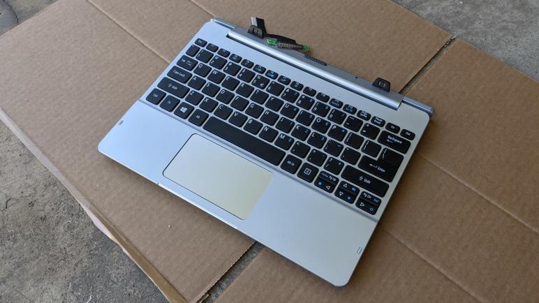
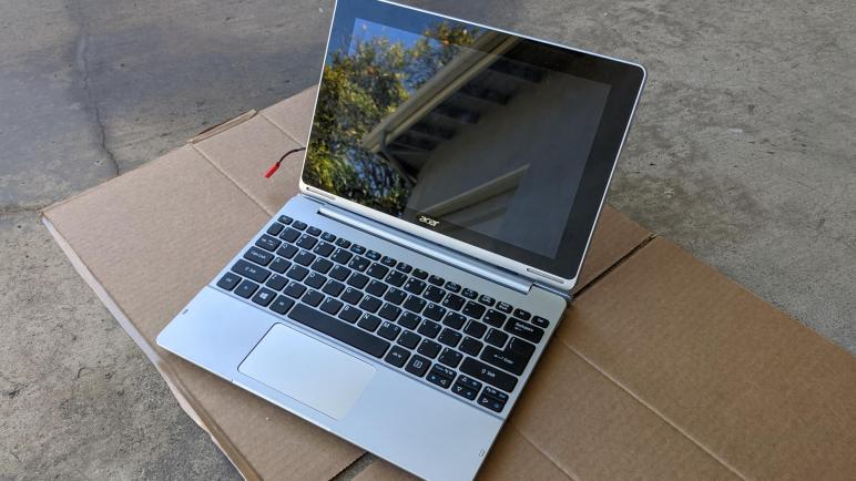
A laptop’s keyboard may be the main interface point with the user, but the hinge mechanism of a laptop computer is an often overlooked critical mechanism that can make or break the entire ownership experience. The challenge is even more profound for tablet/laptop convertibles like this Acer Aspire Switch 10 (SW5-012) since it had to detach as well. Digging into this mechanism as part of my teardown unveiled a very intricate but also extremely robust piece of mechanical engineering.

The first challenge is, of course, figuring out where to start opening it up. I pried on the back plate hoping it would pop loose. It did, sort of, in a irreversible and destructive way.

But with it open, I could tell there’s an angled metal spine to this hinge and there are probably fasteners hiding under the rubbery material that cushions the main display unit when it is attached to this base.

The two rubbery cushions were held with double sided tape. Once peeled off, each exposed two screws that helped hold the top plate in place. They’re not the only fastening mechanism, though, there were many other places where the top plate held on for its life and it did not come loose willingly. I ended up breaking it into several pieces.

Top plate removal exposed many more fasteners, several of which held the backplate.

And the remaining fasteners held the metal spine to the bottom section. This is easily the highest density of screws in this machine holding everything together, reinforcing the critical nature of this component.

I finally freed the nine-conductor pogo connector that was one of my objectives for taking this retired computer apart. There are also a few magnets that held the display module in place as a simple and elegant “Acer Smart Hinge”. They will also be salvaged for potential future fun.

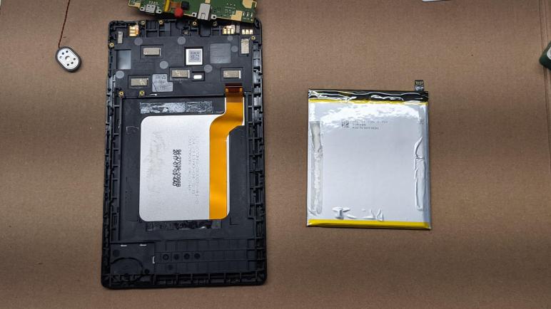
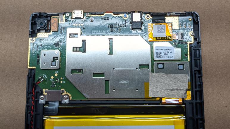
And now with the hinge thoroughly taken apart, I retrieved the main module which had been baking in the sun in preparation for fighting annoying glue.

Acer Aspire Switch 10 (SW5-012) Keyboard

There were two high density circuit boards in the base of an Acer Aspire Switch 10 (SW5-012) tablet/laptop convertible. One handled general connectivity to the main display unit of the computer, and another purely focused on touchpad input. The third, while technically a circuit board as well, is less dense and is the array of switches that implement the keyboard of this machine.

Typing on this keyboard has been a good experience, at least as far as membrane keyboards go. Key travel felt good, and the scissor mechanism sturdily held actions crisp. Even though this is a thin and light (very much so for its day, and still respectably so today) convertible, it never felt flimsy. As I dig inside, I could see what gave it such a solid feel: metal structural plates and lots of mounting points.

The sheer number of mounting points make it rigid, but they are not held with removable fasteners. They are held with plastic rivets probably for cost of manufacturing, but this also meant there’s no way to nondestructively replace the keyboard module. I start by peeling the keyboard surround from the metal chassis plate. Pop, pop, pop, went those rivets as I pulled.

Once the keyboard surround was removed, I could see a magnet that I can harvest (below where the right arrow key used to be) and the remainder will become plastic landfill. The keyboard itself is held to the metal plate by even more plastic rivets, and once I pop them off to remove the keyboard the metal plate should be clean enough for general scrap metal.

Here is a closeup of the control key in the lower left corner, and the numerous gray plastic rivets holding the keyboard module in place.

I popped off the control keycap to take a closer look at the scissor mechanism on this keyboard. I imagine there are only a few major suppliers/styles for this mechanism, unless there’s a product differentiation I’m ignorant about motivating keyboard makers to custom design their own. In any case, my interest was seeing if I can cannibalize the scissor mechanism to repair a missing key on the HP Mini (110-1134CL) netbook from NUCC.

Sadly while the two scissors mechanisms are very similar to each other, they are not identical. Perhaps someone skilled with modifying watchmaker–level mechanisms can hack the pieces to fit, but that is beyond my skill level today. I’ll leave this keyboard alone for now and switch focus to this computer’s robust hinge mechanism.

Acer Aspire Switch 10 (SW5-012) Base Circuitry

When I looked at the reinforcement rib network on the bottom plate I just pulled off, I saw it was not symmetric. The reason became clear when I looked at the internal circuitry of this keyboard base, those asymmetric gaps in reinforcement ribs were to make room for a circuit board and the data cables connecting it to the keyboard array.

Two large connectors dominate the center of this board, one with four conductors and another with five. These nine conductors directly connect to the nine pogo pins connecting to the main unit of this computer. If there were only four conductors I would have been tempted to see if it was direct USB, but there are nine conductors and I don’t have a good idea what might be going on.

I thought the USB hypothesis had merit when I found one of the ICs on board is a USB hub controller. It would have been a valid way to implement this keyboard base: turn the keyboard, the touchpad, and the USB port into individual USB devices connected to a common hub. But USB isn’t a protocol I’ve worked with, it works at far higher speed than any diagnostics tools I have on hand, and I’m not particularly motivated to get this running because if I did, what would I get? A keyboard and a mouse pointer device. I already have enough of those.

So I continued to merrily tear things apart looking for interesting sights as I went. The other circuit board in the base is entirely dedicated to the touchpad. The controller IC on this board is from Synaptics, a very popular supplier for touch hardware. The metal frame came apart in two separate pieces.

It works as a hinge to act against a physical button handling taps on this touchpad. I’m amused that there’s only a single button, they must correlate this button with finger positions in order to infer left or right click.

Flipping it over, I see the cosmetically perfect top surface of the touchpad.

As is typical of touchpads, that top surface is merely a façade covering a network of electrical wires that is used by the Synaptics IC to sense finger position. This is analog voodoo I don’t understand in the least, and neither do most other people, which is why companies like Acer pay Synaptics to figure out. The façade is a sticker that I could peel off to expose the circuit pattern below.

Yep, it’s an array of repeated patterns. Yep, the individual elements will help determine position of our fingers. Beyond those generalities, I have no clue. I’ve taken apart many laptop touchpad like this, and no two has used the same pattern on their circuit boards. Voodoo, I say! Thankfully, with its array of on/off switches, a keyboard is more straightforward than the analog magic of a touchpad.

Acer Aspire Switch 10 (SW5-012) Bottom Plate

The Acer Aspire Switch 10 (SW5-012) was a Windows 8 convertible tablet/laptop that easily separated into two parts. For my teardown purposes, this meant I could work on the keyboard base while the main display module is sitting in the sun to soften the glue holding it together.

When this computer is in laptop mode, the main module communicates with its keyboard base through these robust-looking pogo connectors. I’m not sure I can find a good way to reuse them, but I’m definitely trying to salvage them intact so I’d have the option in the future. It was pretty trivial to pull the top part, and extracting its counterpart from this base is my current objective.

I flipped the base over and saw several straightforward Philips screws. Laptop fasteners are usually hidden, or require an annoying esoteric tool, so this was a delightful surprise. I pulled out a screwdriver, removed (almost) all of them and pulled off the base plate.

A loud crack announced the fact that there were actually two more screws hidden under a gray strip of plastic, and pulling the base apart destroyed plastic around these hidden screws. I’m glad I have no intention of putting this thing back together into working order.

Flipping the bottom plate over, we can see the internal structure. It has a surprising complex of reinforcement ribs. Interestingly, the network is not symmetric. Not top-bottom, and not left-right, yet it speaks to a clear purpose that was not obvious from just looking at this piece.

In any case, these reinforcement ribs reminded me that this laptop, as small and thin as it was, never felt flimsy or gave the impression it would flex and break apart in my hands. Credit goes to reinforcement ribs like these and other thoughtful touches scattered throughout the design of this tablet.

There are two pieces of shiny metal that appear to serve no immediate purpose, my guess is that they are counterweights like I tend to see in other tablet/laptop convertibles. The one on the right has a thin strip of plastic as electrical insulation so it doesn’t short out the circuitry, and those circuit boards are likely the reason why reinforcement ribs are not symmetric.

Acer Aspire Switch 10 (SW5-012) Teardown

With the successful relight of a salvaged Amazon Fire tablet backlight, I’m ready to begin the final chapter of my journey with this Acer Aspire Switch 10 (SW5-012). I’m not the original owner of this machine, so it was never my day-to-day computer. It was retired when it would no longer power-up, and the charger has been lost in the time it was sitting around gathering dust. That nonworking state was how I got it as something to play with.

I diagnosed the power-up problem to a loose cable, and I worked around the lost charger with a hacked-up power connector. That was enough for me to power this system back up. I found it didn’t want to run Linux, but it could run modern Windows 10 surprisingly well. And I didn’t even have to buy another Windows license, as the Windows 8 license embedded in hardware seemed to work just fine. And I undertook some projects like removing its webcam module for security. Because no hacker on the internet can activate a webcam that’s sitting detached in a zip lock bag in another room.

But a computer that runs modern Windows 10 “surprisingly well” for its age is not the same as a computer that runs it well in a useful sense. It’s still an old computer showing its age across the board. Limited RAM, cramped storage, and most personally unsatisfying for me, a low resolution screen. The CPU is not the ill-fated Clover Trail series, but it is still quite slow and is a 32-bit only CPU cut off from modern features of 64-bit operating systems. 32-bit support has already been dropped by MacOS, Ubuntu, even Chrome OS is 64-bit only nowadays.

Finally the system failed again, with the familiar symptom of failing to power up when the power button is pressed. However, this time it was not the loose cable and I failed to find another explanation. It was then retired and I performed a partial disassembly, pulling out its mainboard for a play with a hot air rework station.

I think it is time for me to finish the teardown the rest of the way. The battery pack has already been freed and I think that two-cell lithium ion pack has a future in another project down the line. That leaves the screen, whose low resolution makes it uninteresting as a display but now with two backlight projects under my belt I’m going to see if I can salvage this backlight. Then I’ll see what else might be interesting to salvage from this machine.

Most of what’s left on this convertible laptop main unit were glued together, and I hate fighting glue which is why it halted my earlier teardown. But I have to do it if I want that backlight, so I started thinking about heating up the module to soften the glue. I used to do this with a heat gun, and with the Amazon Fire tablet I used the heated print bed of a retired 3D printer. But we’re now entering the uncomfortably hot phase of Southern California summer. So there’s no need to consume electricity: I can just set this thing out on a brick and let it warm up in the sun and turn my attention to the base section.

Amazon Fire SR043KL Backlight Layers

I took apart an Amazon Fire tablet (SR043KL) retired by cracked touch digitizer glass, seeking to salvage its display backlight and I was successful. I am fascinated by the optical behavior of modern LED backlights, even those used in products with a low price target like this tablet. After fussing with light diffusers for my Glow Flow project, I have a great deal of appreciation and respect for how evenly these backlights distributed their LED light.

I had a lot of time invested in the earlier LG laptop backlight project and was timid about fully exploring all its backlight layers, fearing that I would break something. Now that I have a smaller backlight with lower stakes, I’m going to take the layers apart and see how they act and interact with each other.

[UPDATE: This Hackaday post A Hacker’s Introduction to DIY Light Guide Plates has more details about these backlight layers, as well as making custom plates out of acrylic sheets with a laser cutter.]

At first glance the layers for this backlight are arranged slightly differently from the LG laptop backlight. I’m too new into this field to guess what tradeoffs are involved. What I do know is that the bottom-most layer on the Fire backlight appears to be non-removable. When acting alone, I could see a dotted pattern almost like dithering.

Above this layer is a sheet of smooth matte translucent white that I would have expected to be the top layer, but here it is.

When in place, it blended the dotted pattern together into something smoother. I think this looks great as-is, but we have two more layers to make it even better.

The third layer looks wild, with the optical characteristics I associate with Fresnel lenses and lenticular lenses, but this pattern looks different and I wished I knew the right name for it so I could read more about it.

When installed, it imparted a bit of pattern along with a rainbow-like sheen.

The fourth and final layer also has that optical property, but dialed back a bit. It also has a matte top finish similar to the second layer.

When in place, we have our backlight, providing an impressively even illumination across the entire area with all light provided by a row of LEDs on just one edge.

Speaking of those LEDs, I count eighteen of them. Given that they start illuminating at around fifteen Volts, my guess is that we’re looking at three parallel strings of six LEDs each. I don’t have anything to accurately clamp current at 3*20=60mA (my bench power supply current limit is only guaranteed to be +/- 10mA) but I estimate that would be somewhere near eighteen volts which makes this barely over one watt at maximum brightness. Pretty neat!

I’m setting this aside for later use. Emily Velasco has said she has a project idea that might make use of a small backlight, so it might go to her instead. If it does, I’m sure we’ll get something really weird and cool out of it because that’s what Emily builds. But in case this backlight isn’t what she needs, I can salvage others so we have alternatives.


UPDATE: Emily Velasco used this backlight in a mini X-ray film viewer.

Amazon Fire SR043KL Display Disassembly

I have taken apart an Amazon Fire tablet (SR043KL) and retrieved the prize I sought: an intact display assembly under the cracked digitizer glass. Though presence or absence of cracks in the LCD wouldn’t have mattered for my project anyway. My objective is actually the backlight behind it.

Just like the LG laptop display I disassembled earlier, this display module is held on all edges by thin precision black tape. Peeling back the tape, I had hoped to find a LED backlight driver as I did on the laptop display, but not this time. There are a few small passive components here, but the backlight driver must be on the mainboard hidden under one of those metal shields.

Lacking an easily accessible LED driver, the next objective is to hunt for the backlight LED circuit itself. I expected them to be the largest traces relative to the other components, and I see two exposed contacts already labelled with + and -. Hmm… could it be that easy? I could do a quick test: since these two points were already exposed, soldering some wires to them were straightforward.

In order to see if the LEDs glow, I peeled back more of the tape. Slowly increasing the voltage, I started seeing a glow at around 15V. Wow, it’s really was that easy.

I have no idea how to drive this LCD array, and I have no intention to learn. My objective for today is the LED backlight. So after I peeled away all black tape around the perimeter, I sliced the high density LCD pixel data ribbon in order to separate the two parts.

There isn’t much more to be said about the LCD array. I was able to peel off the polarizer film, this time without cracking any glass, but using acetone to clean off the adhesive once again caused the film to disintegrate. That’s two strikes against acetone, I’ll have to try something else next time.

I have to put more thought into polarizer film recovery, but that’s only a mild distraction from my fascination with the backlight and its sheets of optical magic.

Amazon Fire SR043KL Screen Removal

Tearing down an Amazon Fire tablet retired due to a broken screen, I removed everything I can from the back hoping to find something that would help me release the front. This was unlikely but I held out hope…. hope that has now been dashed. There are no secret back door entrances, I have to fight the double-sided adhesive strips protecting the front door. For me, this is the least enjoyable part of electronics teardowns. There’s no clever puzzle-solving in tearing glued pieces apart, it’s just brute force messy nastiness.

I have not yet developed the knack to do this gently. If the touch digitizer glass wasn’t cracked before, I’m sure it would have cracked after I tried to pry it free. Thankfully it was already cracked, so this was merely even more cracked. And I’m thankful for the clear packing tape I applied earlier, they were able to hold most of the pieces together. If you are planning to tackle this task and wanted to see how much glue you’ll need to fight, this pictures should help.

What was my reward for all this work? The intact display screen module underneath the (now extremely cracked) touch digitizer glass. I had feared it was held by its own adhesives, but the Amazon engineers apparently decided the adhesive on touch digitizer is enough to keep both of these components in place. The screen was held by only a few thin strips of tape, and here I am thankful I removed the battery earlier as it allowed me to push from the back and pop it free.

There was a side bonus here: the tablet chassis held two small magnets. Probably for a tablet screen cover accessory, but now I want to free them. The good news is that I don’t care about preserving the tablet chassis, the bad news is that magnets are brittle and can break under stress. I misjudged how thick they were and broke one. But now I knew they were thin and only held by a strip of double-sided tape, I was able to use a thin blade and cut the other free while keeping it intact.

Once the magnets were recovered, there was nothing else I wanted from this tablet chassis frame and it will head towards landfill while I examine my prize: the LCD module.

Amazon Fire SR043KL Battery and Digitizer Cable

After I moved the mainboard more-or-less out of the way, my next objective was to remove the glued-in battery. This is not just annoying, it is potentially dangerous as lithium polymer pouch batteries like these aren’t very fond of gross physical abuse. And they have a history of protesting their displeasure with a fireworks show in your face! There were two ways forward: I could leave it alone and hope it doesn’t block anything important, or I can remove it now to uncover whatever is underneath and remove a point of volatility from the project. I decided to remove it.

The battery is pretty much surrounded on all sides, but I saw Amazon engineers left a small opening as an entry point. Here it is marked after the fact.

I didn’t see an applicable tool in my iFixit repair toolkit, so I cut apart a piece of thermoformed plastic packaging for a thin and flexible spatula to dig in. I found the bottom strip of tape, and after that I was freed, I could work my way around to free the battery from the remaining three strips. That is a total of four strips of double-sided tape, one for each edge of the battery.

Thankfully the battery did not explode in my face, but I’m not entirely sure it came out unscathed, either. There were some very definitely flexing as I pulled it freed from these four tape strips, because at the time I didn’t know exactly where they all were. Perhaps with a bit of hindsight I could free the battery while putting less stress on it, but I could at least document my findings so maybe the next person who sees this can treat their battery better.


During all of this yanking and pulling of battery removal, I flexed the touch digitizer cable one too many times and it broke. Oops. Well, at least now the mainboard has been completely freed from the case.

Earlier I thought this Kapton-covered segment might have been soldered to the board and didn’t want to pull too hard. Now that I’m no longer worried about damaging this already-damaged part, I stabbed a flat tool in there to release the bond. It turns out there was no soldering, just a piece of tenacious double-sided tape.

There were a few other trivial items accessible from the back of the tablet, including the external speaker, microphones, and switches for external buttons. I was moderately curious about these items, but I had actually hoped to find something that would help me release components on the front side of the tablet. Alas, I found nothing, which meant there’s only one thing to do: start fighting glue.

Amazon Fire SR043KL Mainboard

I’m tearing apart an Amazon Fire tablet (SR043KL) with cracked front glass, and knowing full well this low-budget device would not have been designed to be easily serviceable. After I popped off the back shell, I quickly ran into things held by adhesives of one type or another. My first focus is to see if I can free the mainboard.

The easiest item to release is the battery connector. Two screws held a reinforcement metal plate and, once those two screws were removed, the battery connector popped free easily. On the right side of the battery, I had to peel off some tape to reveal a fairly standard connector for these ubiquitous Kapton yellow flexible circuit boards. The rear facing camera connector easily popped free, but peeling it away from double-sided tape holding it in place took more effort. On the upper-right corner was an enigma. I would eventually learn this was the cable for the touch digitizer glass panel, but after I freed the small connector nothing came loose. The large yellow square was held tight and I didn’t want to pry too hard in case it was soldered underneath to something. I left this for later.

After I removed every visible screw, the mainboard remained stubbornly in place. Poking and prodding all around, I eventually noticed these two plastic claws.

Once freed from these claws, I could flip the mainboard over, still connected by the black touch digitizer cable I had yet to remove.

From here we can see metal reinforcement for the USB port and audio jack, each held down by two screws on either side of the corresponding socket. I think the red rubbery part is a cap over the microphone, next to the front-facing camera module. Springy metal fingers make contact with parts on the chassis. From left to right they are: power button (only two out of three contacts are used), the volume up/down buttons (only three out of four contacts used) and the WiFi/Bluetooth antenna. (All three contacts used.)

I had hoped there would be something interesting to see on this side of the board, but no luck. The opposite side is mostly hidden under soldered-on metal shielding, I think I need a heat plate to remove them nicely. For the moment, components on the mainboard would have to remain a mystery. So I set it aside and started working on a stubborn battery, accidentally severing the touch digitizer cable while doing so.

Amazon Fire SR043KL Teardown Begins

Encouraged by my success salvaging an useful backlight from a cracked laptop screen, I pulled out another cracked screen from my pile of retired electronics destined for teardown. Today’s subject: an Amazon Fire tablet, model SR043KL which appears to translate to the now-obsolete 7-th generation(*) of the product line.

The primary goal of these devices are to put an Amazon shopping portal into our hands, and thus the hardware cost has been subsidized in the expectation of future sales. This was made quite explicit with the bargain “With Special Offers” edition that display more ads than the standard edition. As a side effect, there is little economic incentive to repair these devices. For example, a replacement touch digitizer glass panel(*) for this tablet costs roughly $25, which is half of the normal price for a new Fire tablet(*). Which, by the way, nobody should pay $50 for because Amazon frequently puts them on sale for less.

I got this tablet from a friend who saw no reason to try to fix something when just the parts cost is at least half the cost of a replacement. And he’s not alone. The demand for repair information is so minimal that not even our trusted resource iFixit offers much help. No teardown, no repair guide, and only a few questions on the forums. For a “better than nothing” resource I poked around to find a teardown guide for a different Fire tablet to get a rough idea of what to expect.

With memories of shattered glass fresh in my mind, my first priority was to put some clear packing tape over the screen. Reducing the likelihood of flying shards of glass if it should break apart under stresses of my prying. Given the lack of serviceability typical of devices built to low price targets, I expect a lot of prying on glued-in parts.

Using trusty tools from iFixit I started digging into the seam between the bright yellow plastic and the front face black plastic.

I would not have been surprised if the colorful backshell was glued in, but thankfully it was not. Merely held by plastic clips all around the perimeter that I could pop free.

The internal volume is dominated by the battery, which is pretty typical of tablets. The battery connector is reliably held in place by two screws that I could release to unplug the battery, but the battery itself is glued in place. Over on the right just above the battery is the screen display cable, but it is held down by tenacious tape. The rear-facing camera looked like it might easily pop out, but it is also held down by tape. The black ribbon cable in the upper right is for the touch digitizer, and it is held down by tenacious double-sided tape. And I see a speaker in the lower left, which is held by… you’ll never guess…

In summary, once we pop off the back cover, there’s little else that can be done without doing something irreversible. Almost everything else would require tearing some adhesives loose. I decided to start with the system mainboard.


(*) Disclosure: As an Amazon Associate I earn from qualifying purchases.

Laptop Backlight Is Now Webcam Light

I have successfully salvaged the backlight module of a LG LP133WF2(SP)(A1) laptop LCD display, which meant in addition to all the lessons I learned along the way, I now have a rectangular ~15″ diagonal LED panel that can emit diffuse white light. What do I do with this light? I looked around at places in my life where I felt I had a lighting challenge, and the most relevant issue in these pandemic times is my webcam for video calls.

Right now my primary workstation is in a room with decent sunshine during the day but only a dim overhead light at night. Resulting in grainy video as the camera struggles to capture limited light, and the position of the light also cast some unfortunate shadows. There is a far stronger light in the room, but it is set up to illuminate my workbench behind me. If I forget to turn that light off during a video call, I can immediately tell there’s a problem because I turn into a silhouette on camera. What I need is a light behind the webcam, which is something I can easily buy. There’s an entire product category for this usually in the form of a ring that surrounds the camera. What I have on hand is a rectangle and not a ring but I still want to try it. To test this idea I’ll need a way to mount the panel on top of my computer monitor.

Since this is supposed to be a quick test, I didn’t want to go full out with CAD and 3D printing. I pulled some cardboard boxes out of the paper recycle bin and happily started cutting with my Canary cutter. It was a highly iterative trial and error process and after a few hours I had a cardboard contraption that held the panel above my monitor, sitting on its top edge.

This top edge mechanism was the trickiest part of the design as it needed to be strong enough to hold the weight of the entire assembly. This assembly was heavier than I had originally planned because I didn’t foresee the very obvious fact the panel would make the assembly top heavy unless I added a counterweight (in the form of a large lithium polymer battery pack) sitting below the lip in order to drop the center of gravity. This is too much weight for just cardboard to hold against, so I had to pull in some plastic to help. But still no 3D printing: I cut up an used-up Starbucks gift card into an inverted U shape to give me the necessary strength at this key junction on top of the monitor.

This is definitely not the final design. I want to move the panel lower and further away from my face so it is directly behind the camera instead of above it. I chose the current panel height because I needed to be able to reach the brightness adjustment knob mounted in the lower left. After I put this box together, I realized I could have easily rotated the panel 180 degrees so the knob is in the top right corner instead of the lower left, allowing me to sink the bottom edge below the camera. Alternatively, I could have the brightness PWM adjustment module as an external module mounted elsewhere.

So that is the first and most significant change I want to make for the next iteration, but I’ll use this cardboard first draft for a little while longer and see what other issues I might want to address. In the meantime I proceed to the next backlight exercise with an Amazon Fire tablet.

Installing Arduino Circuit, Round 2

I have a small circuit board to generate a PWM signal that tells the TPS61187 LED driver chip how bright to illuminate the LED of a backlight I salvaged from a cracked LG laptop LCD screen model LP133WF2(SP)(A1). It’s not the most compact thing I could have built, but it was simple and quick. Or at least it was supposed to be quick, because my first attempt at installing it destroyed a solder connection to the screen control board and I had to redo my soldering joints and secure them with hot glue in the hopes I wouldn’t destroy any more solder connections.

Now I’m installing the circuit board again, and I realized I forgot a very important detail: The location I wanted to mount this thing is on the metal frame of this backlight, because I didn’t want to block any light that might emit from the plastic back side of the panel. My circuit board had many soldered connections on the bottom. Putting soldered connections on a metal plate causes short circuits! Fortunately I realized this before destroying anything.

Adding to the bulk of this project, I placed a sheet of clear plastic packing tape as the first layer of insulation, followed by two layers of double-sided foam tape to raise it off the first layer. The foam tape wasn’t as secure as I had hoped, so I warmed up the hot glue gun again to squirt out some secure standoffs. Thanks to the first layer of clear packing tape, I’m semi-confident I can replace this with a different PWM generator if I decide to do so in the future. But for the moment I have completed all electrical work for this light panel that I can power off USB. A happy end result of a lot of very useful and valuable electronics lessons learned building this project. From reading datasheets and their schematics to figuring out what to do when things go wrong.

But the happy result does have one downside. When I have a failure, I can dispose of the pieces after thanking them for their valuable lessons. But when I have a success, I can’t just throw it out! So now I have a ~15″ diagonal rectangular LED light and I need to think of something useful to do with it.

Need Backup Plan For TPS61187 Interface

I had thought I was near the finish line for my backlight revival project, but then I tugged on one wire a little bit too hard and destroyed the circuit board test point I had soldered to.

This is bad, and it got worse. As I tried to gently unwind this LED_EN wire, it was not gentle enough and the soldered points for Vin and GND started unraveling as well. For those two wires I had soldered to either end of a (relatively) large surface mount decoupling capacitor bridging those two voltage planes, because the tops of these capacitors presented a metallic surface area for me to solder to. I had thought they were metal end pieces, but they were actually a thin layer of metal that I just learned would peel under stress. The good news was that I was able to melt the solder and remove those wires before they did any permanent damage, the bad news is that I’ll need another approach for these connections as well.

Since I’ve already proved to be clumsy with three out of four wires, I pulled out my hot glue gun to better secure my solder points starting with my PWM wire that still remains. I dropped a dollop of hot glue and, as I pulled my hot glue gun away, I felt the now-dreaded “pop” sensation in my fingertip holding the wire in place. I think I just lifted the PWM copper pad, too! Fortunately, my meter said I still had electrical continuity. So even if I did lift the pad, it is still connected, held in position by my drop of hot glue. But just in case I needed it, I probed around the board and managed to find a backup location for the PWM signal next to the main display control chip.

Backing up further, I found another test point to the left of the LED_EN test point I destroyed. It was labeled VLED and it was connected to the backlight supply voltage line. As fragile as these test points have proven to be, I think they’re still better than the end of a surface mount capacitor. I’ll use this one and hope I don’t rip this one out as well. Finding a replacement location to solder to the ground plane was easy, as the entire circuit board shared a common ground plane and I had many choices for ground. Including the metal housing of the now-unused data connector that formerly connected to the rest of the laptop. So I’m not worried about a ground connection, I have a plan C, D, E, F, etc. For now I found what looks like a test data bus will use the ground pad for that.

Which leaves me with the original problem: the LED EN pad that I’ve destroyed. I had no luck finding another test point, and while I expect it is connected to one of the pins on the main LG Display ANX2804 chip, I couldn’t find a good contact point for that either. Then I remembered the TPS61187 datasheet, where it said it was valid to connect EN to VDDIO which will cause the chip to be enabled whenever it receives power on Vin. From my notes probing the components around the chip, I knew there were some surface mount components adjacent to each other. They are tiny, but I was able to get a short length of wire to solder across those two components. Since I won’t be tugging on this wire, I should be OK here.

After I verified the VDDIO and EN pins are now connected, I realized there was another way: Since these two pins are adjacent to each other on the TPS61187 itself, a blob of solder can theoretically bridge those two pins right on the TPS61187. I’ll keep that in mind as a potential plan C if I should need it.

To minimize the chances I’ll need any of those backup-to-the-backup plans, I became very generous with my hot glue application. I sincerely hope I won’t have to take this apart again, because I don’t see how I can undo all this hot glue without destroying these solder points.

Fortunately I wouldn’t have to undo anything because my second attempt at system integration was a success.

Installing Arduino Circuit Caused Setback

I didn’t understand why I couldn’t pull USB power through the existing jack on my Arduino Nano, but I was willing to create a small circuit board to wire up VUSB directly as a workaround and move on. I originally soldered two 0.1″ headers next to each other for power and ground, but the first test run instantly pulled those wires out of the socket. So I wired up JST-XH connector for that beheaded USB cable instead. I wanted a connection more mechanically secure than the generic 0.1″ headers and towards that goal I used JST-XH 4-conductor connector. Even though I needed just two conductors, I wanted the wider connector for two reasons. (1) I hoped a wider connector will latch more securely, and (2) I was running low on 2- and 3- conductor connectors in my assortment box. (*)

Next to the power input connector is the potentiometer(*), now soldered and fixed to this perforated prototype board instead of dangling off somewhere via wires. I plan to mount this board on the sheet metal backing of the light, near the lower left corner so the knob for this potentiometer can be accessible.

Next we have the two rows used for seating an Arduino Nano. Even though I’m only using four pins, I soldered all the points on these two rows so this header will sit securely. I had originally thought I would run wires around the outside of these headers, but it turns out I could put all the wires, resistors, etc. in between these two rows so I did that. I doubt it makes much of a cosmetic difference.

And finally, the star of the show, my four-conductor connector to the wires I’ve soldered to various points on the LG LP133WF2(SP)(A1) LCD panel control circuit board. The connector is standard hobbyist stuff, relatively large and easy to work with for my projects. But the other end of the wires soldered to points on the control circuit board which were quite a bit smaller, so I had been concerned about the strength of my soldered joints. And when I lifted the connector to plug into my newly created perf board, I heard a “pop” and knew instantly that was bad news. I had destroyed the LED_EN connection. It was intended as a test point so it was small, but I had soldered to the tiny circle of copper and handling this circuit placed too much stress on this connection. The wire I added ripped off the copper pad, leaving non-conductive (and non-useful) bare circuit board material behind. This is not good. I need a backup plan.


(*) Disclosure: As an Amazon Associate I earn from qualifying purchases.

Arduino Nano Failed to Power Backlight via USB

It was fun to look at a revived LED backlight module, salvaged from a LG laptop display panel model LP133WF2(SP)(A1). It was controlled from a breadboard Arduino, and powered by my bench power supply. I’m still unsure what input voltage it was originally designed for, but it seemed to run well at 5V. When I turned brightness up to maximum, the bench power supply reported 1A of current draw. As a 5W LED light, it does feel approximately in the same ballpark as the 7W LED bulbs serving as 60W incandescent bulb replacements. But with the key and very valuable difference of the fact its light is evenly distributed across a much large area for a softer more diffuse light.

While I’m at it, I measured the electrical behavior of these LED strings. This is mostly for reference since the TPS61187 chip handles adjusting these voltage values to keep electricity flowing at the target current. When it sees a very minimal PWM signal, I measure the voltage drop from anode to ground to be roughly 15V and the panel is not visibly illuminated at this low level. When I turn the duty cycle up high enough to see just a little bit of visible illumination, the voltage differential has climbed to 24V. At max power, I measured about 28V. This was all generated by the onboard boost converter from a 5V input signal. In my experience white LEDs drop roughly 2.7-3V at full power, so these values are consistent with parallel LED strings of either nine or ten LEDs per string.,

Since this circuit seemed to run at 5V, I thought it would be fun to convert this to run on USB. The Arduino Nano was designed to run on 5V and already had a handy USB jack, and most portable USB power banks can supply 5V@1A or at least they claim to. When I hooked up the wires, it was able to illuminate up to a certain level. But beyond that level (roughly 1/4 to 1/3 brightness) the lights started flickering in a classic sign of power instability. Oops. What went wrong?

Whenever I see potential sign of power instability, my first reaction is always to perform the Big Honkin’ Capacitor test. Find the biggest capacitor I have handy, connect it across the power input terminals, and see if that solves the problem. In this case, the big capacitor failed to soothe the system.

Digging into schematics for an official Arduino Nano, I see that the VUSB line is not directly connected to the +5V output pin. There are a few components in the way, relating to power control and regulation. The Arduino Nano could be powered via its VIN pin. Following Arduino Uno barrel jack precedence, the input voltage is usually recommended to be 9V. When this happens, there’s a diode presumably to make sure that 9V does not feed back into the USB +V line. There are also several capacitors in parallel with VUSB but they should help rather than interfere with any instability.

Mystified as to why I couldn’t power the backlight via this Arduino Nano’s USB jack, I wanted to isolate the problem. See if the problem lies within the Arduino Nano or with my USB power bank. I took a USB cable and cut off its a damaged micro-B connector. Splaying out the wires, I found VUSB and GND wires, and I connected that to the Arduino Nano circuit. With this arrangement, my backlight module is happy all the way up to full brightness with no flickering problem.

Something about this particular (non-genuine) Arduino Nano module is causing interference, and I don’t understand why, but at least I have a workaround. That’s enough for me to ignore this weirdness today and proceed with my backlight project, even if there was a temporary setback.

A Closer Look at LED Backlight Panel

I’ve successfully interfaced with the existing TPS61187 driver chip on the circuit board of a LG laptop display panel LP133WF2(SP)(A1), and brought the backlight module back to life. Given all the new territory I had to explore to get this far, I was very excited by a successful initial test. After I was able to calm down, I settled down to take a closer look at its physical/optical behavior.

Since I tested it face-down, the easiest thing to look at first are the backsides of the LED strip. Most of it is hidden by the sheet metal frame from this side, but from earlier examination I knew there was even less to see from the front. Once illuminated, we can see the structure inside the light strip. The yellow flexible segment that connects to the green circuit board isn’t a separate piece like I thought earlier, it is actually all a single sheet of flexible circuit. All the LEDs are mounted on it, and they are located at the very bottom edges of the screen. I knew the lights themselves had to be very thin and well hidden right up against the bottom edge, but I couldn’t figure out where the wiring would go. Now we can see all electrical wiring runs above the LEDs, and when we look at it from the front we can see it as a thin strip of light gray along the bottom.

I had been worried that the illumination would be compromised because it is working without some of the friends it had earlier. The backside used to have a laptop lid that would have helped reflect and diffuse light. And the front used to be up against the LCD pixel array, which was backed by a mirror finish that would have also helped reflect light around.

I need not have worried. It was quite evenly illuminated and, as seen in the wire shadow picture above, there are no distinct spotlights marking location of individual LEDs.

I also wondered if the surprisingly complex four-layer diffuser required precise alignment with the LEDs in order to do their light distribution magic. They are no longer pressed by the LCD pixel array into a tight space, but happily they still worked quite well. While they worked visibly best at certain positions, the falloff is graceful. Not like aiming a laser at precision optics. Now I’m even more impressed by this stuff performing magic with light in ways I don’t understand.

But one thing I do understand is that they look thin and quite fragile. Designed to sit behind a LCD panel of multiple glass layers and without that, these layers of magical optical sheets flap around. I looked around and found a piece of 3mm clear acrylic that is nearly the perfect size and taped it to the metal backing chassis. The acrylic is far thicker than the LCD glass sandwich used to be, but it is also more rigid, so that’s a good tradeoff.

The final comparison I wanted to make before moving on is: how bright is the backlight alone compared to the full backlight plus LCD screen? I placed this backlight, turned brightness all the way up high, and set it side-by-side with the intact replacement screen still serving display duty in the Chromebook. I then turned on the Chromebook and increased its screen brightness to maximum setting.

I don’t have light level measurement instruments to obtain an objective number, but this picture makes it quite clear there is a dramatic difference in brightness. I knew some light would have been lost within the layers of a LCD panel, but it’s fun to see firsthand it’s far more than I had expected. This really drove home why alternate display technologies with self-illuminating pixels (OLED, micro-LED, etc.) can offer much brighter pictures than a backlit LCD could. My salvaged backlight is plenty bright running on just 5V, but running it on USB took more effort than expected.

Arduino Nano PWM Signal for TPS61187 LED Driver

Trying to revive the LED backlight from a LG Lp133WF2(SP)(A1) laptop display panel, I am focused on a TPS61187 LED driver chip on its integrated circuit board. After studying its datasheet, I soldered a few wires to key parts of the circuit and applied power, checking the circuit as I went. Nothing has gone obviously wrong yet, so the final step is to give that driver chip a PWM signal to dictate brightness.

This is where I am happy I’ve added Arduino to my toolbox, because I was able to whip up a controllable PWM signal generator in minutes. Putting an Arduino Nano onto a breadboard, I wired up a potentiometer to act as interactive input. 5V power and ground were shared with the panel, and one of the PWM-capable output pins was connected to the TPS61187 PWM input line via a 10 kΩ resistor as per datasheet. I found that my enable line already had a 1 kΩ resistor on board, so now I wired enable directly to the 5V line.

Since I wanted some confidence in my circuit before plugging the panel into the circuit, I also wired a test LED in parallel with the PWM signal line. I had originally thought I could use the LED already on board the Arduino, but that is hard-wired to pin 13 which is not one of the PWM-capable pins, so the external LED was necessary for me to run my PWM-generating test code, which thanks to the Arduino framework was as easy as:

int sensorPin = A0;    // select the input pin for the potentiometer
int ledPin = 3;        // select the pin for the LED
int sensorValue = 0;   // variable to store the value coming from the sensor

void setup() {
  // declare the ledPin as an OUTPUT:
  pinMode(ledPin, OUTPUT);
}

void loop() {
  // read potentiometer position
  sensorValue = analogRead(sensorPin);

  // map analogRead() range to analogWrite() range
  sensorValue = map(sensorValue, 0, 1023, 0, 255);

  analogWrite(ledPin, sensorValue);
}

My external test LED brightened and dimmed in response to potentiometer knob turns, so that looked good. My heart started racing as I connected the panel to my Arduino breadboard, which is then connected to my benchtop power supply. Even though I’m powering this system with 5V, I used a bench power supply instead of a USB port. Because I didn’t know how much the panel drew and didn’t want to risk damaging my computer. Also, by using a benchtop power supply I could monitor the current draw and also set a limit of 120mA (20mA spread across 6 strings) for the first test.

I powered up the system with the potentiometer set to minimum, then slowly started turning the knob clockwise…

It lit up! It lit up! Woohoo!

I was very excited at this success, jumping and running down the hallway. It was a wild few minutes before I could settle down and calmly take a closer look.

Soldering Wires to TPS61187 LED Driver

After passively studying its documentation, and passively studying how it is installed on an existing circuit board, it is now time for me to go active and start working on it. Whether I can get this backlight up and running is almost secondary at this point, it has already been a great electronics learning opportunity and I want to see how far I can get.

This next step tests my skill working with components far smaller than what I’m used to. The picture of these added wires spoke volumes: I used the finest spools of wire I had on hand, but 26 gauge wire looks absolutely gargantuan when soldered to this board. Due to their small size I assumed these surface mount components would not have the strength to handle external stresses. As a temporary measure I used a piece of tape to hold the wires in place, hopefully diverting all the little twists and tugs yet to come as I connect and disconnect these wires to power and signal sources.

Once the wires were in place, I had to make a very important decision: what voltage do I feed into the Vin wire? Earlier probing failed to find the values of resistors used in the boost converter feedback regulation circuit. If I had those resistance values I could hoped to calculate the expected input voltage range using the formula in the datasheet. The only other guideline I had was the requirement that input voltage must be lower than the voltage drop across individual LED strings so the boost converter (critical part of this circuit) can function.

Looking for hints elsewhere, I reviewed my earlier notes looking inside this machine. Its battery is labeled as a lithium-ion pack with a nominal voltage of 10.8V, implying three cells in series. This is within the valid input range for a TPS61187 chip and I thought it is possible they would wire the battery voltage straight through. This would avoid any conversion losses from a boost or a buck converter along the way.

Following my startup plan, I used my bench power supply to put 10.8V on Vin and was encouraged I didn’t see any sparks or smell any smoke. My probe saw 5V on VDDIO which I took to be a good sign and satisfies step 1. Moving on to step 2, I checked enable (EN) pin to find it is low, so nothing else on the board is raising it. I used a one kilo-Ohm (1 kΩ) resistor to pull EN high and it did, so either nothing else on the board is pulling it low or 1 kΩ is enough to overrule their signal. If something is fruitlessly trying to pull it low, the few milliamps involved here should not damage it. Or if I do damage it, hopefully it wouldn’t be anything I care about.

If I understand the datasheet correctly, once enabled the TPS61187 will put minimum voltage across the LED strings. I probed the voltage between LED common anode and ground, and found it was 6.7V, which is lower than the input voltage of 10.8V, exactly what the datasheet said not to do. Oh no! I quickly turned the input voltage down to 6V so it would be below the LED voltage, wondering if it was already too late. There were no obvious signs of damage so… whether I’ve just killed it or not, my next step is to put a PWM signal on the brightness control line.

Finding TPS61187 LED Driver Interfaces

I want to reuse the TPS61187 LED Driver IC already on board the display circuit board of a LG LP133WF2(SP)(A1) laptop LCD panel. Driving the backlight that used to shine from behind the now-cracked LCD screen. After studying the datasheet and probed around the circuit board to understand how the chip is configured, I am now probing to see where I can solder wires to interface with the chip.

There are two major concerns here. The first is that I’m learning to work with modern consumer electronics, with circuit boards populated by very small surface mount components. Most of the resistors and capacitors I probed earlier are barely larger than the tip of my soldering iron’s finest tip. The “normal” tip is comically large next to these things. If I continue with experiments like this I will need to buy my own hot air station and learn to use it well.

The second concern are the other components on this control board. If I supply voltage and ground to the TPS61187, the rest of the circuit will probably come alive in some way I don’t understand. I’m not worried about them draining a bit of battery, that’s the best case scenario. I’m more worried about them interfering with the backlight control signals for enable (EN) and brightness (PWM).

First target is to find a place to inject power. The datasheet told me where the power pins are on this chip, but it’s far too small for me to hand solder myself. I’m not saying it’s impossible to hand solder to them, I’m just saying it’s very difficult and unlikely to succeed with my current skill level. So I went poking around nearby components looking for a decoupling capacitor. Because this driver IC uses a boost converter circuit to raise the voltage to drive the backlight LEDs, I expect to find a sizable decoupling capacitor nearby to isolate the rest of this board from the electrical noise of boost conversion. I found one adjacent to the inductor. For a surface-mounted component, it is large and thankfully big enough for me to feel confident I could solder to its two ends for VIN and GND.

I found a resistor and capacitor nearby connected to the enable pin. But even though they are larger than the corresponding TPS61187 pin I couldn’t solder to them. I was able to connect to one side of the small capacitor, but an intended-to-be-gentle test tug ripped off the wire taking a corner chunk of the capacitor with it. Oops, not so gentle after all.

I had even less luck finding a PWM signal connection near the TPS61187. I could see its pin connection on the circuit board, but it instantly sank out of sight to one of the other layers of the board and I found no place nearby where it surfaced.

After some thought, I decided to look for these signals near the largest chip sitting on the other end of the board, labelled “LG Display ANX2804”. I reasoned that EN and PWM are probably controlled from this chip and perhaps I could find something. There was nothing obvious near the chip itself, but I struck gold on the backside of the board. Sitting effectively under the ANX2804 are several labelled and accessible test points, and I was happy to see “LED_EN” next to one pad and “PWM” next to another. (There’s also VLED visible further left I didn’t notice until later, which should be better than soldering to the VIN end of a surface mount decoupling capacitor.)

Continuity test confirmed these do connect all the way across this thin strip of circuit board to the TPS61187, I think we are in business! Time to do some soldering.