HP Windows Mixed Reality Salvaged LED Pinout

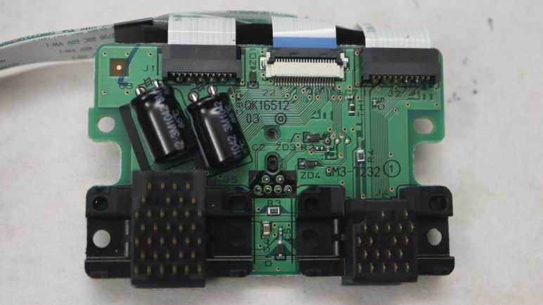
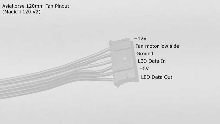
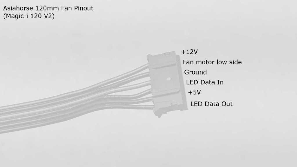
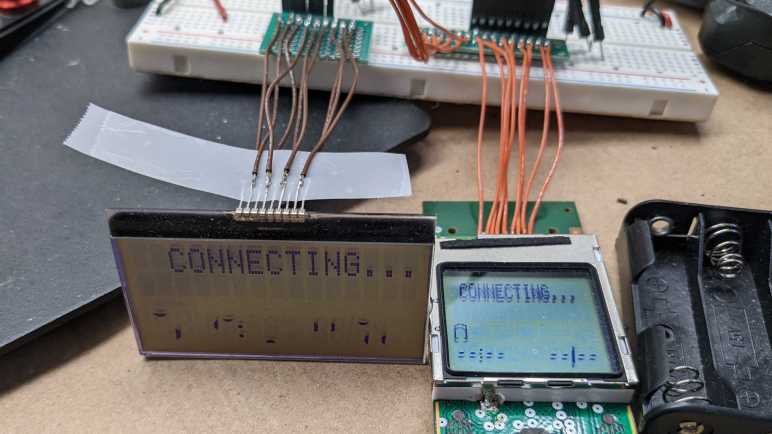
While doing a bit of work bench clean up, I found the LED arrays I had intended to salvage from my HP Windows Mixed Reality headset teardown. The surface mount LEDs were soldered on flexible circuit boards so they’re a bit too fragile for me to just toss them in a plastic bag. I found a piece of cardboard to serve as a backing and that should help. Before I put them away folded between sheets of cardboard, I thought I’d pull out my LED tester. Here’s what I found out about their pinout, in the hopes such information will be helpful for future project planning.

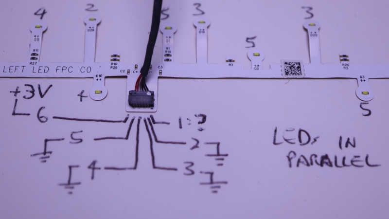
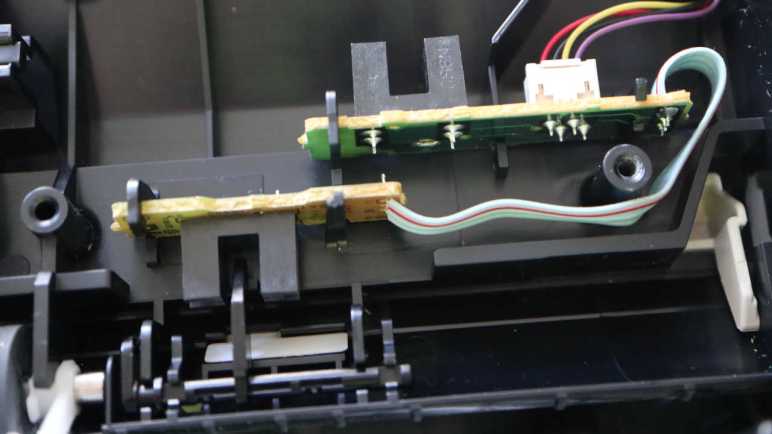
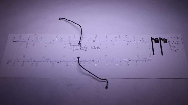
The two long strips came from handheld controller location beacon rings. Their shapes are symmetrically mirrored between left and right hand controllers, but they both use the same electrical connector. I saw a small arrow and decided that was pin 1, but it didn’t seem to connect to anything? Pin 6 is the common positive power supply, and pins 2 through 5 are grounds, one for each of four strings. Each string of LEDs are wired in parallel, so 3V is enough to start illuminating them with 20mA shared across all LEDs. There are resistors visible on board so current limiting seems to already exist if I’m ready to crank up the voltage. The LEDs are labeled D1 through D32. I had guessed these 32 LEDs would be evenly divided among 4 strings for 8 LEDs each, but it’s actually two strings of 7 and two strings of 9.

Connector Pin#LED StartLED EndLED Count
2D26D327
3D19D257
4D10D189
5D1D99

Using my mini hot plate I also salvaged the cable PCB connectors. I don’t know if I will use them, but I have the option to do so if I want. At the moment I’m not sure how I might utilize these two very irregularly shaped string of LEDs.

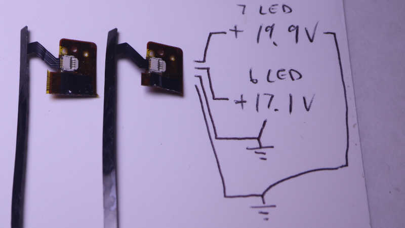
The two short strips came from visor LCD backlights. I wanted to keep the entire backlight display but it was so thin and delicate I failed to disassemble them intact. These LED strips are my consolation prize. Two identical units, one for each eye. Four pins on the connector for two LED strings, but again they are not equally sized. The inner pair powers a string of 6 white LEDs in series, around 17.1V DC for 20mA. The outer pair powers a string of 7 white LEDs in series, around 19.9V for 20mA. I don’t see current limiting resistors here so something else will have to keep things under control.

I thought about using my hot plate to pull these connectors from the flex circuit board as well, but decided to use scissors to cut off most of the flex circuit board and keep the connectors attached. I think this pair of ex-backlight LEDs will work well as PCB side lights, once I can think of a good design for a light-up PCB holder.

Mazda Mirror (Auto Dimming with HomeLink) Pinout

Once I completed a radiator (and radiator hose) replacement for my 2004 Mazda RX-8, I moved on to another item that has been sitting on the to-do list for many years. At one point I was excited to add a dashcam to my car, and thought I could do a clean job of integrating one because a wiring harness already exists high and center on my windshield for my fancy rearview mirror. At night it automatically dims in response to bright lights behind me, and it has a HomeLink remote control with three function buttons. (One of which is worn out because I use it for my garage opener.) I saw the same mirror installed across the Mazda lineup so it is not a RX-8 exclusive feature.

Many years ago I visited a RX-8 at a local salvage yard for an unrelated project and picked up an extra fancy mirror along with a segment of its wiring harness. I figured it would help me experiment with how to tap power from its counterpart in my car. It sat until today, when online resources included Mazda wiring diagrams for reference. I didn’t have to determine the pinout experimentally, I could just look it up.

Only four wires were used in this 10-position connector. All four had black insulation, but three of them had a thin color stripe for identification. The Mazda diagram labeled the wire positions A (upper right in picture above), B (lower right), through J. The four wires were:

Position B has a black wire with no color stripe. This wire provides +12V power only when ignition is in the “On” position. This ensures auto-dimming feature doesn’t waste energy when the car is parked.

Position D has a black wire with green stripe. This wire provides +12V power only when reverse gear is engaged. I’m not sure why this is here. Perhaps auto-dimming is disabled when I’m backing up? I never noticed one way or another.

Position F has a black wire with yellow stripe. This is the ground wire.

Position J has a black wire with red stripe. This wire always has +12V power for the HomeLink transmitter.

Whenever I get around to the dashcam installation, I would first try using the black (ignition on) wire for power. Unless the camera storage may get corrupted by abrupt shutdown. In that case, I will use black/red (always on) for power and use black (ignition on) wire as inverted signal to finish writing to storage and perform a proper shutdown. But honestly I don’t think it’s going to happen.

MX340 Print Carriage Encoder Pinout

It took some digging, but I finally reached the circuit board inside the print carriage of my old Canon Pixma MX340 multi-function inkjet. Most of it is dedicated to print cartridge connectivity (or more specifically, their integrated print heads) but I don’t care about that.

I wanted to know which (of many) wires connect to the optical quadrature encoder buried in its center.

It is not identical to the optical quadrature encoder used on the paper feed roller, but they look closely related. Potentially upright (reads encoder disc perpendicular to the circuit board) vs. flat (reads encoder strip parallel to the circuit board) versions of the same device.

More relevant is the fact they seem to share the same circuit board footprint with their arrangement of six pins. Trying the easy thing first, I pulled out my multimeter and used the paper feed encoder as a guide to probe the pins on the print carriage encoder. I quickly confirmed they have the exact same pinout.

One pin is connected to incoming power supply, and onward through some resistance to another pin. I measured the resistance at a little over 80 Ohms which is not a typical resistor value. I suspect it’s actually a higher common value (maybe 100 Ohm) but some components in parallel brought down the effective value. The A/B phase signal wires are out at the ends, and the remaining two pins are grounded.

I traced the two signal wires and the power supply wire to the rightmost three pins of the ribbon connector. I didn’t put a number on ground because multiple pins (like pin 15) are connected to ground.

The pin numbers were taken from the system main board, which labeled pin 1 with a number and an arrow (the end closer to camera) and for this cable the other end gets a “22” label (far end, circled in red.)

I had hoped finding these pins would tell me how to tap into its communication on the mainboard side, but they turned out to be the wires most buried and difficult to access. Ah well, I’ll solder my probe wires to the print carriage circuit board instead.


This teardown ran far longer than I originally thought it would. Click here to rewind back to where this adventure started.

Canon Pixma MX340 Control Panel Connector to Main Board Pinout

There was no shortage of surprises as I’m learning from the control panel circuit board of a Canon Pixma MX340 multi-function inkjet. I followed a wire that I thought supplied power to multiple components, found it powered just a single LED, then realizing the LED on/off is actually controlled by a transistor further down the line. Weird! Fortunately the remaining pins on this connector (for ribbon cable to main board) were easier to understand, enough for me to generate a medium-confidence pinout chart.

Connector to main board pin 11 was soldered to a trace that went under the connector and out the top side. Tracing its path through a zero-ohm jumper resistor (JP117), a few check points (CP102, CP112), an unpopulated capacitor position (C110) and a 220 ohm resistor (R101) I arrived at the “Stop” button (SW101) at the control panel’s far right edge. Canon engineers decided a user trying to stop something in a panic should have a direct line to the main board bypassing the NEC K13988 intermediary.

Connector to main board pin 3 was connected to a capacitor (C116) to ground typical of a decoupling capacitor, and a 470 ohm resistor (R104) typical for LED current limiting. Upon initial examination I thought it might lead to one of the LEDs, but I’ve accounted for all LEDs by now so I know it isn’t that. I traced its route through CP114 and CP126 to arrive at K13988 pin 29.

Connector to main board pin 2 and pin 1 traveled side-by-side, but received slightly different treatments. Pin 2 signal had to travel through a 100 ohm resistor (R103) while pin 1 signal did not. Pin 2 also had a capacitor (C115) to ground while the pin 1 equivalent position (C114) is unpopulated. When they reached the K13988 chip, main board connector pin 1 signal went to K13988 pin 16, and main board pin 2 went to K13988 pin 18.

Pin numbering is right-to-left in the picture, as per arrow and number 1 printed adjacent to the right end of the connector. There is also a dot every 5 pins to aid in counting. After tracking down all of these traces, I repeated the exercise with pins connected to the K13988 chip.

Pin NumberConnection
1 (arrow)K13988 pin 16
(Main board to K13988 asynchronous serial 250000 8E1)
2K13988 pin 18
(K13988 to main board asynchronous serial 250000 8E1)
3K13988 pin 29
(K13988 Chip Enable)
4Ground
5 (dot)Alarm LED+ @ 3.3V DC
6Power LED+ @ 3.3V DC
7Power button
(Grounded when pressed)
8Ground
93.3V DC power
(Always on, even in standby)
10 (dot)Ground
11Stop button
(Grounded when pressed)
12WiFi LED+ @ 5.5V DC
(Illumination controlled via transistor Q101.)

This teardown ran far longer than I originally thought it would. Click here for the starting point.

Canon Pixma MX340 Control Panel LCD Connector

I have a Canon Pixma MX340 multi-function inkjet in a partially disassembled state, still running, and I’m learning how it works. Looking at the control panel, I was encouraged by how much I could learn just by looking at the connector to the main board, so I will keep going and look at its LCD screen connector.

The first challenge is the LCD interface connector is even smaller and denser. My experience had been hobbyist-level electronics for a breadboard with pins 0.1″ (~2.54mm) apart. The main board connector had just 1mm between pins, over double the density. This LCD connector doubles density again, with only 0.5mm between pins. Those thin copper traces were hard to see so I took my picture and exaggerated its contrast. Bright parts are now overblown and dark detail crushed, but the traces are much easier to see now and that’s what’s important today.

Since Canon engineers thoughtfully labeled pin 1 with an arrow and number, I know to count pins right-to-left. The first thing to do is look for traces larger than the rest, usually indicating power/ground wires. I see three instances of two pins wired together: 6+7, 8+9, and 10+11. Visually following the copper traces, I found LCD pins 6+7 connected to mainboard pin 9 that delivers 3.3V even in standby mode. LCD 8+9 is connected to mainboard pin 10, the curiously thin ground pin. (LCD draw very little current, so that is consistent with the hypothesis pin 10 serves low power draw components.) C100 is the decoupling capacitor between those power and ground planes.

LCD pins 10+11 didn’t go very far: they led to capacitor C101, the other side of which is ground. In fact, looking at that patch of copper, five more capacitors (C105 through C109 inclusive) connect corresponding LCD pins (19 through 23 inclusive) to ground. Working towards the right, C104 sits between LCD pins 17 and 16. C103 between LCD pins 15 and 14. C102 between LCD pins 14 and 13. I’ve seen LCD modules use external capacitors before, but this is a much larger capacitor network.

I don’t see any traces going under the connector out the other side, so pins 12 and 18 are either unconnected or connected to one of the copper patches that run under the connector. One patch is ground, to which the connector’s chassis pins soldered to. There’s a smaller patch, which supplies power to pin 24.

This tiny super dense connector was intimidating at first glance, but as it turned out an explanation can be found within 3cm for majority of those pins. Only 5 pins out of 24 require further exploration.

[UPDATE: I now have information on pins 1 through 5, which connects to NEC K13988 chip on the circuit board. Table has been updated accordingly.]

Pin numberConnection
1NEC K13988 pin 28
2NEC K13988 pin 26
3NEC K13988 pin 27
4NEC K13988 pin 9
5NEC K13988 pin 10
63.3V DC
73.3V DC
8Ground
9Ground
10C101 to ground
11C101 to ground
123.3V, ground, or not connected
13C102 to 14
14C102 to 13 and C103 to 15
15C103 to 14
16C104 to 17
17C104 to 16
183.3V, ground, or not connected
19C105 to ground
20C106 to ground
21C107 to ground
22C108 to ground
23C109 to ground
243.3V DC

This teardown ran far longer than I originally thought it would. Click here for the starting point.

Canon Pixma MX340 Scanner Image Sensor Pinout

Taking apart a Canon Pixma MX340 multi-function inkjet, I wanted to see what I could learn from its scanner’s CIS (contact image sensor) bar. Expectations weren’t high at the start but after spending some time looking at its behavior under an oscilloscope I think I understand enough to explain every pin on its cable connector.

I’m arbitrarily numbering these pins from left-to-right in this picture. I don’t have Canon’s electronic schematic or engineering data, so this might be reversed from Canon’s actual pin ordering. I feel confident about the accuracy of red labels, I’m more tentative about the pins labeled in blue.

The first five pins support illumination. There are separate pins for red/blue/green LEDs and they all shine onto a common light guide that disperses across the sensor bar.

  1. 5.5V DC power source as common LED anode.
  2. Red LED cathode.
  3. Green LED cathode.
  4. Blue LED cathode.
  5. Chassis ground.

The remaining seven pins support image sensor data.

  1. Data clock (tentative) at 2.37538MHz with amplitude of 3.3V. Clock signals are normally square waves. This one is very nearly a smooth sine wave but I guess it still counts?
  2. Line sync+ (tentative) at 425.543Hz. Raised up to ~3.3V for one data clock cycle to signal new scan line, read on falling edge of clock signal. Low voltage level fluctuates relative to chassis ground, but is in sync with line sync- and should be compared against that.
  3. Line sync-. Reference base for pin 7 line sync+.
  4. 3.3V DC power source for image sensor logic.
  5. Power ground for image sensor logic.
  6. Analog pixel data+ (tentative). Raised up to ~3.3V above chassis ground (or roughly 2V above reference base pin analog pixel data-) to indicate brightly lit pixel. Drops to less than 0.1V above reference base for both dark pixels and overblown pixels. Drops under reference base in the non-data periods at the beginning and end of each scan line.
  7. Analog pixel data- (tentative). Reference base for pin 11 analog pixel data+. Voltage level is roughly 1.0V above chassis ground but fluctuates in sync with analog pixel+ approximately +/- 0.1V.

All of this information were inferred from using either a multimeter or an oscilloscope to observe voltage levels on each pin, while the printer is either going through its startup sequence or sitting idle. This doesn’t tell us which component is responsible for which signal. For example, while pin 11 analog pixel data is certain to come from the sensor bar, this data doesn’t tell us if the clock signal on pin 6 comes from the sensor bar or from the printer main board. That’s just the first of many barriers against repurposing this sensor bar.


This teardown ran far longer than I originally thought it would. Click here for the starting point.

Canon Pixma MX340 ADF Sensors

I’m diving into the electronic guts of a partially disassembled Canon Pixma MX340 multi-function inkjet, starting from the top: the automatic document feeder (ADF).

Inside the paper feed mechanism is a pair of sensors that appear to be photo-interrupter switches.

I see a simple circuit board and through-hole components, so it looked like an easy starting point. There were no fasteners holding these two circuit boards in place, just cleverly shaped plastic molded into the body. A four-wire harness connects this sensor assembly to the main board. I see wires colored red, black, yellow, and purple. I guessed they would be power, ground, signal 1 and signal 2. (I was wrong.)

Here’s front and back of the sensor that senses when a document has been placed in the ADF. Looking at the back, I see a tiny surface-mount resistor labeled R51 and marked with “471” for 47 * 101 = 470 Ohms. This is a common value used for a LED current-limiting resistor, so that implies the associated pin is emitter LED power and the adjacent pin ground. Which makes sense, as it was routed to one of the pins of the receiver as well. Process of elimination says the final pin should be the sensor signal.

Turning the printer on, my hypothesis was verified with the volt meter. When light between the emitter and receiver is blocked, the sensor signal is at 3.3V. Probably pulled up by something on the mainboard. When there is no blockage between the emitter and receiver, the sensor signal pin is pulled to ground.

Given the 3.3 volts I detected on the signal wire, I had expected power to be 3.3V as well and was mildly surprised to measure 5.5V on that wire. Why go through the complexity of having multiple voltage planes? Maybe the engineers thought it would better to have higher voltage running through the long skinny wire from mainboard to sensor. But if so, why not use 24V DC directly from the power supply and use a bigger current-limiting resistor? 5.5V must present a useful tradeoff between 3.3V and 24V but I don’t know those Canon engineers’ considerations.

The other sensor detects whether a sheet of paper has been successfully fed into the ADF mechanism. It seems to use the same photo-interrupter sensor and the circuit works similarly.

Working back to the long 4-wire harness, I was surprised to discover my initial guess on wire assignments were backwards from the actual measured behavior.

RedBlackYellowPurple
ExpectedPowerGroundSignalSignal
ActualSignal 1Signal 2Ground+5.5V DC Power

I guess Canon doesn’t care much for wire color convention, where red is usually power and black for ground. Alternatively, maybe this was a production hiccup that inadvertently reversed the color order loaded on the wire harness machine. Maybe the relevant Canon engineering team decided: “Well, it is wired right electrically, so we’ll just ship with the wrong wire colors.” A valid choice! The end user never sees these wires and would never care about their color anyway. Maybe the story is documented in an errata for Canon technicians that I would never see.

That’s fine, I got what I came here for. Next up: the ADF motor.


This teardown ran far longer than I originally thought it would. Click here for the starting point.

FormLabs Form 1+ OLED Pinout

I have a broken FormLabs Form 1+ laser resin 3D printer and I’m learning what I can from taking it apart. On its front panel is a small OLED dot-matrix display that I have been exploring. I have now successfully controlled that OLED module using an ESP8266 development board.

Confirming the speculation in this FormLabs forum thread, the OLED module is very similar to the Newhaven Display International NHD-2.23-12832UCB3. Both of their display areas are 2.23″ diagonal with 128×32 pixels of resolution. They both use a SSD1305 controller, but while Newhaven’s module provided a single row of 20 pins, FormLabs custom built their own circuit board connecting to the rest of the printer with a 10-wire IDC ribbon cable. Only 7 wires are actually used.

This OLED module is also very similar to Adafruit product #2675 Monochrome 2.3″ 128×32 OLED Graphic Display Module Kit but without Adafruit luxuries like 5V logic level shifter and power buffering capacitor.

This module only requires a power supply of 3.3V DC, because it has an onboard voltage boost converter to supply other voltages needed by OLED. All logic high signals are also 3.3V DC. Data communication is via SPI protocol with an additional command/data select input wire. When that wire low, the chip will interpret SPI traffic as commands and when high, SPI traffic will be sent to graphics frame buffer.

  1. Ground
  2. Vcc to supply 3.3V DC
  3. Command/Data select
  4. SPI Clock
  5. Reset (Active Low)
  6. SPI Data In (*)
  7. SPI Chip Select (Active Low)
  8. Unused
  9. Unused, but connected to mainboard I2C bus data line
  10. Unused, but connected to mainboard I2C bus clock line

(*) There is no SPI Data Out pin.


Now this pinout is documented, I will explore side curiosities like potential OLED burn-in.

Pinout for Asiahorse 120mm Fan (Magic-i 120 V2)

The Asiahorse Magic-i 120 V2 bundle included three 120mm cooling fans with integrated addressable RGB LEDs. These fans have a six-wire connector designed to be plugged into a hub that was included in the bundle, along with a remote control to change the light shown performed by those LEDs. Most users just need to plug those fans into the included hub, but some users like myself want to bypass the hub and control each fan directly. For this audience, I present the fan connector pinout derived from an exploratory session on my electronics workbench.

Since this was reverse engineered without original design documents, I don’t know which side is considered “pin #1” by the engineers who designed this system. These connectors appear to be JST-PH, whose datasheet does point to one side as “Circuit #1”. But there’s no guarantee the engineers followed JST convention. To avoid potential confusion, I’ll call them only by name.

NameSystemComments
+12VFanHigh side of fan motor. Hub connects this wire directly to +12V power input.
Motor LowFanLow side of fan motor. Use a power transistor between this wire and ground to control fan speed.
GroundFan + LEDPower return for LED circuit and can be used for fan motor low side as well. Hub connects this wire directly to power input ground.
Data InLEDInput control signal for addressable RGB LED. Compatible with WS2812/”NeoPixel” protocol.
+5VLEDPower for LED circuit. Hub connects this wire directly to +5V power input.
Data OutLEDControl signal for addressable RGB LED beyond the end of LED string inside the fan. Useful for chaining multiple units together by connecting this wire to Data In of the next device in line.

Now that I understand its pinout, I will build my own control circuit to replace the default Asiahorse hub.

LCD Driver Pinout for Honda CD

After a few wrong turns, I think I have a good grasp of the interface for talking with the audio (CD player) portion of a Honda Accord dashboard. This circuit board also includes HVAC (heating/ventilation/air conditioning) controls, though I investigated only their knobs and ignored the electronics. This page is a summary of my investigation into interfacing with audio controls.

Electrical

There are at least three independent circuits present.

  1. Panel backlight using small incandescent (filament) bulbs with a blue cover. Draws 0.6A at14.4V DC.
  2. LCD backlight draws 0.2A at 14.4V DC.
  3. Digital communication with Sanyo LC75883 LCD driver chip, which is a 5V part. We can send data to control LCD segment display and use it to read data for most of the button presses.
PinLabelDescription
1LAMP+BPower for panel light bulbs, up to +14.4V relative to LAMP-RET.
2LAMP+BPower for panel light bulbs, up to +14.4V relative to LAMP-RET.
3LAMP-RETReturn for panel light bulbs.
4LAMP-RETReturn for panel light bulbs.
5LCDLAMP+BPower for LCD backlight, up to +14.4V relative to LCDLAMP-RET.
6LCDLAMP-RETReturn for LCD backlight.
7P-GNDGround.
8P-GNDGround.
9P-GNDGround.
10IS BUS FRAMEUnknown.
11IS BUS DATAUnknown.
12CD-LEDUnknown.
13IGN-DETUnknown. (Ignition Detect?)
14SWD-VDD+5V power supply for LC75883.
15D-GND(Digital?) ground.
16LCD-DIData in from LC75883 chip. (Wired to LC75883 DO pin.)
17LCD-DOData out to LC75883 chip. (Wired to LC75883 DI pin.)
18LCD-CLKLC75883 Clock.
19LCD-RSTLC75883 Resets when pulled to 0V. Pull to 5V for normal operation, do not leave floating.
20LCD-CELC75883 Chip Enable.
21ENC VOL-DNOne of two quadrature encoder phases for central audio control knob.
22ENC VOL-UPOne of two quadrature encoder phases for central audio control knob.
23EJECTNormally open, shorts to ground when “Eject” button is pressed.
24PW SWNormally open, shorts to ground when “Power” button is pressed.

Digital

All control for LCD segment and key scanning for most of the buttons are handled by a Sanyo LC75883 chip. It communicates with a Sany proprietary protocol called CCB (Computer Control Bus) that has some resemblance to I2C or SPI but is neither. It listens on address 0x42 for bits indicating which LCD segments should be active, and reports on address 0x43 indicating which buttons were pressed. I have an Arduino sketch (target device: AVR ATmega328P based Arduino Nano) that demonstrates how to interact with the LC75883. Pressing the “Mode” button will cycle between the basic “turn all segments on” program, a bit pattern “drawing” program, and an animated demo.


This Arduino sketch for this investigation is publicly available on GitHub.

Preliminary Pinout for Honda CD

I have a Honda in-dash CD (and HVAC) control board and I want to see if I can make its LCD work. After I melted through conformal coating over the Sanyo LC75883 LCD driver chip, I was able to get an electrical connection with my meter so I can test for continuity between the pins (that are too fine for me to solder) to something I can more easily work with. I quickly found that much of the CD player functionality is connected to a small black rectangular connector I noticed earlier. Not just the LCD driver chip’s data communication lines, but also the big central rotary knob and button.

There is a large degree of uncertainty here, because I didn’t find what all of the pins did. I also found two pins that both appear to be ground, and I don’t know if there’s an important distinction between those two pins. This incomplete understanding explains the problems I will encounter later.

Using the numbers on the circuit board silkscreen, the pins are 1 to 24 from right to left. (Silkscreen shows 1 in the upper right, 2 in the lower right, 23 in the upper left, and 24 in the lower left.)

PinPreliminary NameDescription
7Vss (?)Either 7 or 9 is ground, maybe both?
9Vss (?)Either 7 or 9 is ground, maybe both?
14Vdd+5V power supply
16DOCCB Data Out
17DICCB Data In
18CLCCB Data Clock
20CECCB Chip Enable
21AEncoder A, connects to ground when knob is at certain positions.
22BEncoder B, connects to ground when knob is at certain positions.
24ButtonConnects to ground when “AUDIO PWR” button is pressed

Once these connections were made, I could make further progress. That is, running into an entirely different set of headaches.

Pinout of LCD Salvaged From AT&T CL84209

When I retired my landline phone connection, I also retired my home phone. It was an AT&T CL84209 phone with built-in digital answering machine. I had a base station and though it supported multiple cordless handsets I had just a single handset. Without a landline, I took the entire system apart keeping a few parts for potential later use. Among the stuff I kept were two custom LCD units. One LCD was freed from the base station circuit board. I wanted to keep its backlight as well, but I accidentally destroyed it while trying to free it from the system. The other LCD was in the handset, and I kept it attached to its circuit board because I didn’t want to accidentally destroy another backlight.

They sat in my pile of salvaged parts for several years, until a few weeks ago when I took them out and started playing with them. I thought I could find some official documentation on these display units, but nothing came out of searches using every identifier I could find on these devices. Fortunately, thanks to the still-working handset circuit board and a logic analyzer, I figured out enough to control them from an ESP8266 Arduino program. This page is a summary of my findings.

Electrical

Both LCDs have nine hardware interface connections. Base station LCD uses pins, handset LCD shown above uses an FPC. I’ve numbered them 1 through 9 counting left to right as we are looking at the display. Despite the different physical form factor, electrically speaking they respond identically.

PinNameAdditional Notes
1EnableWe can make it always enabled by tying it high: use a 1kΩ pull-up resistor connected to pin 5 (+3.3V)
2SCLI2C clock logic level measured +3.3V, don’t know if it is +5V tolerant.
3SDAI2C data logic level measured +3.3V, don’t know if it is +5V tolerant.
4GroundRelative to pin 5
5VccSupply +3.3V to this pin.
0.82uF capacitor between this pin and pin 6 (Vboost)
6VboostOutput pin of built-in boost converter. Measured at +5.4V.
0.82uF capacitor between this pin and pin 5 (Vcc)
7VLCDHLCD segment voltage (high) 8kHz square wave from Vcc to Vboost
0.82uF capacitor between this pin and pin 8 (VLCDL)
8VLCDLLCD segment voltage (low) 8kHz square wave from 0V to Vcc
0.82uF capacitor between this pin and pin 7 (VLCDH)
9Voltage measured to match Vboost
Appears not connected to anything else on handset circuit board.

Digital

Both LCDs are I2C devices with an address of 0x3E. There are two types of messages:

  • Configuration set of 8 messages. Values were copied from logic analyzer capture and played back. Their exact meanings are unknown.
  • Data set of 3 messages. First message includes 15 bytes of alphanumeric data for the first line, second message for the second line, and the third message has 16 bits of digital data toggling state of custom LCD segments. (Which are different between LCDs.)

See the following pages for details:


Source code of software written to help with this investigation is publicly available on GitHub.

Pinout of Tape Deck Faceplate (Toyota 86120-08010)

It is time to wrap up investigation into the workings of a tape deck faceplate, salvaged from the stock audio head unit of a 1998 Toyota Camry LE. I believe I’ve deciphered all the information necessary to reuse this faceplate independently from the rest of the tape deck. Summarized in this pinout report with links to more details.

The faceplate circuit board is largely built around a Sanyo LC75853N chip, which communicates via a Sanyo proprietary protocol called CCB (Computer Control Bus). An external microcontroller (I used an Arduino Nano in experiments to date) can dictate what is displayed on the LCD (see segment map here) and scan pressed/not-pressed state of buttons (see button map here).

Some faceplate components are independent of LC75853N:

From right-to-left, functionality I observed on these pins are:

LabelFunction
ACC5VPower supply for digital logic.
+5V relative to GND
LCD-DOCCB digital data out.
LC75853N address 0x43
Single 4-byte transmission to microcontroller.
LCD-DICCB digital data in.
Microcontroller to LC75853N address 0x42.
Three 7-byte transmissions to LC75853N.
LCD-CLKCCB clock signal.
Active-low generated by microcontroller.
LCD-CECCB enable.
Active-high generated by microcontroller.
CD-EJEEject button.
Normally open, shorts to GND when “Eject” button is pressed.
ILLIllumination power supply (positive).
+5V to +14.4V (~60mA) relative to ILL- for variable button backlight brightness.
LCD-BLLCD backlight power supply (positive).
+6V (~60mA) relative to BL-
VOL.CONVolume control potentiometer.
Voltage between ACC5V (full clockwise) and GND (full counterclockwise)
PULS-AAudio mode quadrature encoder knob – A
ACC5V or GND, will be opposite of B when at a detent.
A and B briefly identical during transition between detents.
PULS-BAudio mode quadrature encoder knob – B
ACC5V or GND, will be opposite of A when at a detent.
A and B briefly identical during transition between detents.
GNDDigital logic power (negative).
Relative to ACC5V
ILL-Illumination power supply (negative)
Relative to ILL
BL-LCD backlight power supply (negative)
Relative to LCD-BL
RESETUnknown. Observed 0V relative to GND.
LC75853N has no reset pin.
Seems OK to leave it unconnected/floating.
Unknown. Observed 0V relative to GND.
Seems OK to leave it unconnected/floating.

Source code for this investigation (and accompanying demo) is publicly available on GitHub.

Sleuthing NEC VSL0010-A VFD Control Pinout

Vacuum Fluorescent Display (VFD) technology used to be the dominant form of electronics display. But once LEDs became cheap and bright enough, they’ve displaced VFDs across much of the electronics industry. Now a VFD is associated with vintage technology, and its distinctive glow has become a novelty in and of itself. Our star attraction today served as display for a timer and tuner unit that plugs into the tape handling unit of a Canon VC-10 camera to turn it into a VCR. A VFD is very age-appropriate for a device that tunes into now-obsolete NTSC video broadcast for recording to now-obsolete VHS magnetic tape.

Obviously, in this age of on-demand internet streaming video, there’s little point in bringing the whole system back to life. But the VFD appears to be in good shape, so in pursuit of that VFD glow, salvage operation began at a SGVHAK meetup.

NEC VSL0010-A VFD Before

We have the luxury of probing it while running, aided by the fact we can see much of its implementation inside the vacuum chamber through clear glass. The far right and left pins are visibly connected to filament wires, probing those pins saw approximately 2.5V AC. We can also see eight grids, each with a visible connection to its corresponding pin. That leaves ten pins to control elements within a grid. Probing the grid and element pins indicate they are being driven by roughly 30V DC. (It was hard to be sure because we didn’t have a constant-on element to probe…. like all VCRs, it was blinking 12:00)

This was enough of a preliminary scouting report for us to proceed with desoldering.

NEC VSL0010-A VFD Unsoldering

Predating RoHS solder that can be finicky, it was quickly freed.

NEC VSL0010-A VFD Freed

Now we can see its back side and, more importantly, its part number which immediately went into a web search on how to control it.

NEC VSL0010-A VFD Rear

The top hit on this query is this StackExchange thread, started by someone who has also salvaged one of these displays and wanted to get it up and running with an Arduino. Sadly the answers were unhelpful and not at all supportive, discouraging the effort with “don’t bother with it”.

We shrugged, undeterred, and continued working to figure it out by ourselves.

NEC VSL0010-A VFD Front

If presented with an unknown VFD in isolation, the biggest unknown would have been what voltage levels to use. But since we have that information from probing earlier, we could proceed with confidence we won’t burn up our VFD. We powered up the filament, then powered up one of the pins visibly connected to a grid and touched each of the remaining ten non-grid pins to see what lights up. For this part of the experiment, we got our 32V DC from the power supply unit of a HP inkjet printer.

We then repeated the ten element probe for each grid, writing down what we’ve found along the way.

NEC VSL0010-A VFD Annotated

We hope to make use of this newfound knowledge in a future project, and we hope this blog post will be found by someone in the future and help them return a VFD to its former glowing glory.