Honda CD Control Detours

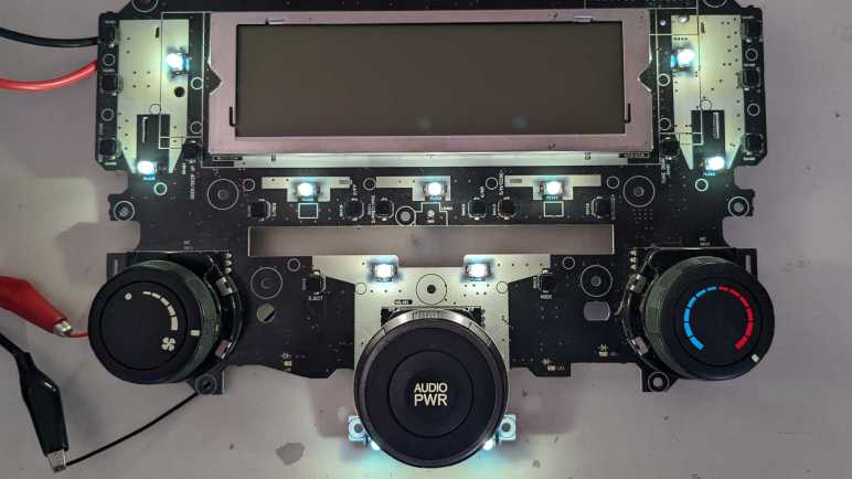
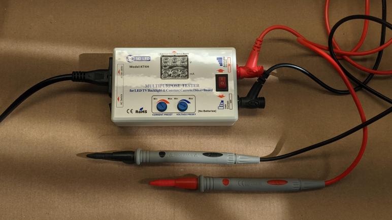
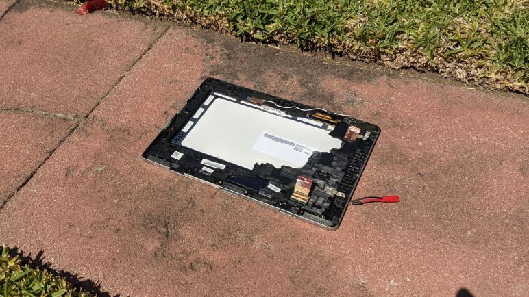
After I finally found my mistake reading a Honda CD control panel’s input (I had left the reset pin floating) I think I have a pretty good handle on communicating with it. The CD audio side, at least, as I had no interest in figuring out the HVAC side. But before I wrap up with a summary and demo, this page describes two additional experiments for future reference.

External Quadrature Encoder

Before I realized my problem was a floating reset pin, I wired in an external quadrature encoder to determine if the problem might be with the Honda circuit board or if it was my code. There was an added bonus that this particular quadrature encoder was designed so that every detent would be high/high. I knew the problem of LCD blanking out was related to grounding various controls (buttons or this knob) to ground, so with its four transitions per detent, this knob would quickly blitz through the problematic states as a workaround.

Successful use of the external knob also meant I now know the LCD wasn’t blanking out due to something in my code, or even something in the Arduino as related to a quadrature encoder. The LCD would blank out if the onboard knob was in the wrong position, even if none of its wired connected to my Arduino. This observation was consistent with the actual cause of a floating reset pin. I removed this external knob once the reset pin was no longer left floating, making room for the next experiment.

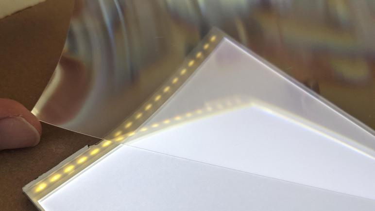
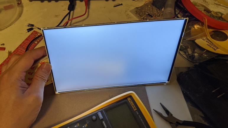
Boost Converter for LCD Backlight

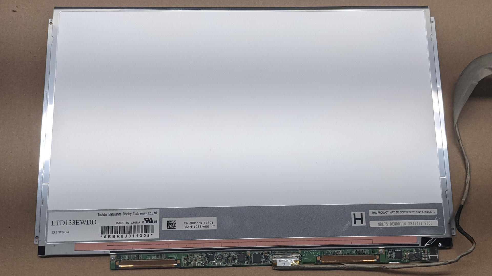
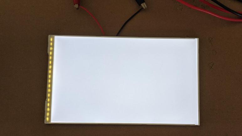
When I had illuminated the LCD backlight using my bench power supply, it indicated the backlight drew 0.2A at 14.4V ~= 3W. I thought that would be within reasonable range for a USB power bank, so I dug up a DC voltage boost converter (*) from a batch I had bought for an earlier project. I connected the voltage input to Arduino VIN pin and adjusted the converter to 14.4V open-circuit output voltage. But when I connected that output to the LCD backlight, voltage sagged and the USB power bank went into a continuous reset loop consistent with overload response.

I wasn’t sure if the overload was a startup issue, a transient issue, or a continuous power issue. As an experiment I soldered 220μF capacitors to both input and output. This did not change the behavior: the USB power bank still enters a continuous reset loop. I added a USB power meter (*) between my power bank and the Arduino and it said the circuit tried to draw 3 amps. Yikes! That explains the reset when I had expected only 0.6 amps (3 watts / 5 volts) to be drawn.

I’ll revisit the LCD backlight power supply issue later, if I decide to reuse this LCD for something fun. At least this failed experiment let me know boost converter power draw is more complex than (Power) = (Voltage)*(Current). It is also another checkmark next to “I should learn how boost converters work” on my to-do list, I hope with such knowledge I could properly diagnose this failure to verify I understand the situation correctly.


(*) Disclosure: As an Amazon Associate I earn from qualifying purchases.

Honda CD Panel Lights and LCD Backlight

When I started this Honda CD control panel investigation, I thought I might still have the CD player mainboard that sat behind the control panel. But when I pawed through my pile of anonymous circuit boards, I didn’t see anything I recognized as related to the CD control panel. After spending time looking at the control panel in detail, I became more familiar with the connector between the control panel and the mainboard. Revisiting the pile with this knowledge, I now recognized the matching connector. But even more importantly, the old mainboard had labels on its connector pins.

Note that both connectors stagger their pins, but confusingly in opposite directions. Pin 1 is lower-right on the mainboard labels, but upper-right on the control board numbering. I hadn’t spent much effort trying to find the pins for control panel illumination, but now that I see these LAMP pins clearly labeled, I wanted to light them up.

The first experiment was to apply +14.4V DC to LAMP+B and ground to LAMP-RET.

When power was applied, all the little incandescent bulbs with blue covers lit up. The color is not as blue as the covers would imply. It actually has a tint of green because those bulb’s natural glow is not white but a warm yellow. If they are supposed to masquerade as blue LEDs, they’re not doing a very convincing job. This collection of 11 bulbs drew 0.6A at 14.4V.

The next test is to put +14.4V DC power to LCDLAMP+B and ground to LCDLAMP-RET.

This illuminated the LCD backlight, drawing 0.2A at 14.4V. It is not very bright, but at least the light is fairly uniform. (Unlike its Toyota tape deck counterpart.) The primary purpose of these backlights is to ensure the display is visible at night. During daylight, these LCDs are legible under ambient sunlight. Lighting these up was fun! This experiment was good reference as I repurpose the connector for my own use.

Chunghwa CLAA133UA01 Circuit Board and LED Backlight

I tried and failed to salvage the polarizer film of a Chunghwa CLAA133UA01 display panel, but that wasn’t the primary objective anyway. I turned to the real goal of salvaging its LED backlight and the first step is to remove the perimeter protective film. Most of my prior salvaged panels were held together with thin black plastic tape, this panel is slightly different in its use of shiny metallic foil tape. I was surprised to see it, as I thought foil would short-circuit the components underneath. Perhaps it is some sort of metallized plastic instead of metal foil. This stuff rips more easily than others but at least its adhesive still came off cleanly.

Once the foil was removed, I could see three important-looking chips on the circuit board.

Closest to the cable connector is a chip marked MST7337F-A AQ2T842B 1049B. A web search found Kynix Semiconductor MST7337 which is a chip for NTSC/PAL/SECAM automotive TV applications. I don’t think this is the right chip, but the correct answer eludes me. I might have better luck if I knew the logo, which is distinctive but not one I recognize. I didn’t see that logo on the Kynix Semiconductor page.

The next chip was marked AAT11771 A2U274 1052. A web search found a hit: Advanced Analog Technology AAT11771 is a controller for driving TFT LCD displays.

The third important-looking chip was marked A706B A38T 66040. Its proximity to the LED backlight connector makes it a prime candidate for the LED driver, it’s even next to the inductor + capacitor pairing consistent with a boost converter to raise voltage high enough to drive strings of LEDs. A search for A706B found that A706 is a standardized grade of steel bars for concrete reinforcement, but I saw nothing about a LED driver chip.

Pulling up the backlight connector for a look, I can see there are five thin conductors, one per contact point plus one thick conductor using three contact points. Remaining contact points between them are apparently unused. Based on what I’ve seen on other panels, I guessed the thick conductor is a common source for five current sinks for five parallel strings of LEDs.

This hypothesis was quickly and easily tested with a LED tester, so if I never manage to find information on that LED driver chip I should at least be able to drive these strings directly via copious test points visible in that area of the circuit board.

Until I find need for another diffused LED light source, this is a good stopping point. I put the LED backlight back into storage and pulled a non-dead panel out of my hardware archives. This one is still attached to a nominally working HP Stream 7 tablet.

Chunghwa CLAA133UA01 Polarizer Glue Stronger Than Polarizer Film

After verifying I could illuminate LED strings of a LG LPP133WH2(TL)(M2) salvaged from a Dell laptop, I set it aside to work on the final panel in my stack of LCD laptop panels. This was salvaged from a Sony VAIO laptop whose model number I no longer know.

The original owner had spilled some cola on it. Good news: the spill did not immediately kill the machine so data could be pulled off averting any loss of data. Bad news: the computer started failing intermittently in strange ways as corrosion took hold, and eventually died a few weeks after the initial spill.

Removing the panel I see a label with designation Chunghwa CLAA133UA01. (Along with some dried coke residue.) Web lookup indicated this is a LED-backlit panel with 1600×900 resolution. Better than the 1366×768 resolution we see on baseline laptops today, but still short of full 1920×1080 resolution. Like the rest of my stack of panels, I decided it was not interesting enough to revive as a display.

My first task was removing the polarizer film in the front of the display, something I have yet to perfect through several past experiments. So far I’ve been able to remove the film in one piece but failed to clean off adhesive residue. For this panel, I didn’t even get that far. This panel used glue that was very strong, apparently stronger than the tensile strength of the polarizer film! Roughly a quarter of the way through peeling, the film tore apart and I decided to abandon polarizer retrieval.

Looking at the tear was mildly interesting. It was a zig-zag pattern instead of a straight line. This material is weakest at plus or minus 45 degrees relative to screen viewing orientation. Does that have any relation to polarization angle, or is it indicative of something else? I don’t have any tools to probe that question so I will set it aside for now and move on to the LED backlight.

LED Backlight of LG LP133WH2 (TL)(M2) Laptop LCD Panel

I’m pulling apart some retired laptop LCD panels. For the latest panel, I decided to work on the polarizer film first and I was encouraged by those results. I’ll probably try the polarizer first for future panels. But before I move on to the next panel, I want to get a closer look at the LED backlight from this panel I pulled from a retired Dell laptop. The label says it is a LG Display LP133WH2 (TL)(M2) module. A quick internet search says its pixel resolution is 1366×768, which is pretty low by today’s standards and not worth the effort to bring back online as a computer display.

Like many previous modules, it had tape all around. Unlike some previous modules, there are several different types of tape involved.

Peeling back the tape, I could see the backlight connector in the center. The previous few panels had them to the side. I’m not sure what design tradeoffs are involved in the different placements.

The chip footprint closest to the backlight connector is unpopulated. This is usually a sign there’s another version of the device with enhanced features, but I’m not sure how that works for a display module like this. Whatever it may be, the absent chip is certainly not the backlight LED controller.

The other chip on this side of the circuit board is labeled LG SW0641A. I’m amused that my not-helpful search results included a LG clothes washer with that model number. I’m not sure what this is, but it is definitely not a clothes washer. It is probably the main display controller that talks to the rest of the laptop.

Flipping the panel over, high density data connectors for the LCD array are visible as well as two chips.

Searching for information on a SiW SW5024, I came across vendors willing to sell them but not much else.

But that doesn’t matter, because a search for ADD 5201 written on the other chip resulted in a pointer to a “High Efficiency, Eight-String White LED Driver for LCD Backlight Applications” by Analog Devices. Jackpot!

While the chip can drive up to eight strings, it appears we only have four on this panel. I see a VOUT_LED test point that fans out to four conductors on this connector. And I also see test points corresponding to four strings. FB1 is to the left, below VOUT_LED. FB2, FB3, and FB4 are to the right. If it follows convention of other panels, VOUT_LED would be the current source and FB1 through FB4 are sinks for each of four parallel strings of LEDs.

Probing those points with a LED tester confirmed the hypothesis, and highlighted another difference on this panel. Previous panels with parallel strings of LEDs would interleave them across the bottom. With an interleaved design a single failed string would still leave most of the display illuminated. But in this panel, each of these four strings are assigned a quarter of the panel area. So if one string failed, one quarter of the display would be darkened and difficult to read. My guess is this method is easier (and cheaper) to wire as a tradeoff for fault tolerance.

With the LED strings verified to illuminate, I set this aside and started working on the final disembodied laptop display panels currently in my possession: a Chunghwa CLAA133UA01 from a Sony VAIO laptop.

Toshiba LTD133EWDD Backlight

Examining the integrated control board on a Toshiba LTD133EWDD panel I had pulled out of a Dell XPS M1330 laptop, I found no information on communicating with its integrated LED driver chip so I’m going ahead with the backup plan of seeing if I could drive the LEDs directly. [NOTE: This was written before Randy commented with a link to the datasheet.] First order of business was to remove the LCD pixel array in front of the backlight. A marvel of miniaturization in its day, now I am no longer interested in its 1280×800 pixel resolution.

A thin strip of black tape around all four edges held the glass sheets in the frame. I admire how it precisely mated up against the edge of the polarizer film. It was either applied by a machine or hands of great skill.

Once the tape was removed, the glass LCD array was held only by the high density data connectors. Before I peeled them off, I noticed one item of interest: I see alignment marks that I don’t recall seeing on previous LCD arrays I had peeled off in this way.

While peeling off the high density pixel data connectors, I was reminded that glass is fragile and easily crack when abused.

Once the LCD pixel array was removed, I returned to examining the LED backlight connection. I see an eight-conductor connector, but only seven wires in the flexible cable. One of which is thicker than the rest. Based on the experience so far, my first guess are six LED strings in parallel sharing a common current supply but with six individual current sinks.

Flipping the circuit board over, I found several sets of six pads on the board. The circular pads look like they were designed for pogo pins on a test rig. The rectangular pads look like they are provisions for decoupling capacitors that were never installed. We could see the top row of six are all connected, consistent with a common supply. The bottom six each correspond to the six current sinks on the connector.

One interesting novelty was that while the leftmost four connectors are strictly in order, the fifth and six conductors were swapped. So if we count the small vias connecting to the connector on the other side in left-to-right order as 1,2,3,4,5,6. The rectangular pads are in the order of 1,2,3,4,6,5. Perhaps this was merely done to make PCB routing easier, but I’m curious if there’s a more profound reason.

Another interesting item of note is the surface mounted switch immediately to the right and below these pads. This switch would not have been user-accessible in the laptop. Even a servicing technician would have to peel off a plastic protective layer before this switch could be flipped. What does it do, and why is it important enough to take the hit of manufacturing parts cost and complexity? I can smell a story here but not enough interest to chase it down.

In my past LED backlight salvage operations, my next step would be to solder some wires to these points and determine the electrical properties of this string. But now I am armed with a dedicated LED backlight tester, and I could put it to work and probe these points directly. There are indeed six parallel strings of 10 LEDs per string. They each drop approximately 32V at 20mA. This is information I could have determined without the dedicated tester, but having the right tool made the job quick and easy.

Once I had these backlight details identified, I could store it away for future project. But it also had some auxiliary items I should take care of first, like a nice metal frame.

Dell XPS M1330 LED Backlight

My detour into laundry machine repair pushed back my LED backlight adventures for a bit, but I’m back on the topic now armed with my new dedicated backlight tester. The next backlight I shall attempt to salvage came from a Dell XPS M1330. This particular Dell product line offered an optional NVIDIA GPU packed into its lightweight chassis. Some engineering tradeoffs had to be made and history has deemed those tradeoffs to be poor as these laptops had a short life expectancy. In the absence of an official story from Dell, the internet consensus is that heat management was insufficient and these laptops cooked themselves after a few years. I was given one such failed unit which I tore down some years ago. I kept its screen and the laptop’s metal lid in case I wanted a rigid metal framework to go with the screen.

The display module itself was a Toshiba LTD133EWDD which had a native resolution of 1280×800 pixels. Not terribly interesting in today’s 1080p world. Certainly not enough motivation for me to buy an adapter to turn it into an external monitor, and hence a good candidate for backlight extraction.

Unlike the previous LCD modules I’ve taken apart, this one doesn’t cover its integrated control board in opaque black tape. Clear plastic is used instead, and I could immediately pick out the characteristic connection to the rest of the display. At the bottom are two of those high density data connections for the LCD pixel array, and towards the right is an 8-conductor connector for the LED backlight. The IC in closest proximity is my candidate for LED backlight controller.

Despite being clear plastic, it was still a little difficult to read the fine print on that chip. But after the plastic was removed I could clearly read “TOKO 61224 A33X” which failed to return any relevant results in a web search. [UPDATE: Randy has better search Kung Fu than I do, and found a datasheet.] Absent documentation I’m not optimistic I could drive the chip as I could a Texas Instruments TPS 61187. So I’ll probably end up trying to power the LEDs in the backlight directly.

Backlight LED Tester

I have successfully salvaged LED backlight diffuser assemblies from three different LCD screens. It gave me the confidence to attempt pulling the backlight out of other LCD screens in my pile of less-used and broken electronics, in the expectation that diffuse white light sources will be more useful than low resolution displays. But before I start merrily tear more panels apart, I wanted to address one particular pain point: deciphering mystery LED strings.

Only one of the three examples so far gave me an easy time, where the LED backlight power planes were clearly marked with + and -. The other two had multi-conductor cables that required a little decoding to find a common anode and cathodes for individual strings, and sometimes a few conductors remained mysterious. I had been doing this work by spending a lot of time probing with a multimeter, then soldering wires to test points, and cautiously putting power on those lines with a bench power supply. This has worked so far, but I knew there was room to make this process faster for future panels.

Enter the dedicated LED backlight tester.

I wanted something that could put current-limited power over a set of probes. This would let me probe LED strings directly in a single-step versus my current multi-step workflow of multimeter, then soldered wires, then bench power supply. I considered buying a set of probes that I can connect directly to my bench power supply, but a quick search for dedicated LED testers found them quite affordable and I made the jump to try one.

Looking over several options on Amazon, I decided to try a SID LED KT4H(*) because it advertised a few extra features I thought might be useful enough to worth the extra cost. It has household AC input so I don’t have to worry about a separate power supply or batteries. Separate numerical displays for voltage and amperage allows me to read both metrics simultaneously. Simple dials for current and voltage limits make the user interface simpler than designs that use infuriating combinations of unintuitive button presses. There’s a switch to toggle between two current limits: the one set by the dial, and 1mA for testing purposes. This is much better than turning the current limit knob back and forth. And finally, it can also test the other side of the system: whether the device’s constant current supply is putting out any power at all.

The package also included a convenient carrying case, in the form of a generic First Aid Kit zippered fabric bag. Not the fanciest branding, it gave me a chuckle, but it should be quite sufficient.

The probes had sharp tips more than precise enough to hit the kind of test points I had been probing with my meter.

For a quick familiarization run, I used this tester on a single 5mm through-hole LED and saw it light up dimly in the 1mA test mode and brightly with current limit set at 20mA. Then I moved on to illuminate the recently-liberated backlight from an AU Optronics B101EAN01.5. A nice feature is that the current limit ramps up gradually: there is a slow (2-4 seconds) ramp-up as the device seeks the correct voltage level to deliver 20mA. In comparison to my bench power supply which will snap to a voltage almost instantly. I’m optimistic the slower ramp-up will prove valuable.

Before I could put this tester to work, though, life threw me a curveball and I had a broken clothes dryer to fix. The LED backlights will have to wait a bit.


(*) Disclosure: As an Amazon Associate I earn from qualifying purchases.

The Great Backlight Liberation Begins

There’s a small market in LCD panel controller boards. When we salvage a panel from a retired laptop, we can enter its model number into eBay. If the panel is used in a high-volume laptop (for example, one of Dell’s consumer Inspiron laptops. Or most Apple MacBooks) then someone is likely selling a driver board that accepts HDMI input and translates it into the signal to control a panel’s integrated electronics.

I had salvaged the panel from one of my old Dell Inspiron laptops and, buying one of these adapter boards for $50, converted it to an external monitor. Eventually it became the onboard screen for Luggable PC Mark I. (Mark II used a commercially available monitor, and stories on both are available here.) A few months after that adventure, I received another retired Inspiron laptop and used its screen for the Portable External Monitor project.

I have several more LCD panels salvaged from retired laptops, but I don’t need very many external monitors. Furthermore, resolutions on these panels were lower than 1920×1080 limiting their utility. It’s hard to justify spending $50 for a circuit board to hack-up converted laptop screens when a Full HD 1920×1080 desktop monitor can be had for about $100.

I had thought it might be interesting to build my own LCD interface boards, but there are several obstacles. One is the requirement to build connectors to carry high-speed raw pixel information, which is tricky to do correctly given the high bandwidth translating to low tolerance for sloppy work. The LVDS (low voltage differential signaling) system doesn’t connect directly to typical microcontroller output pins, but translator chips are available and some task-specific microcontrollers have integrated LVDS output.

But the biggest hurdle against building my own boards is documentation. The protocol carrying that high-speed raw pixel information is a mystery. Counter to popular electronics convention, datasheets for panels aren’t distributed freely online. Many of them are proprietary and difficult to get, others lie behind paywalls. It makes sense to pay if I’m designing a device using millions of panels, but it doesn’t make sense if I’m fiddling with a single panel.

So those salvaged LCD panels have sat in my workshop, gathering dust waiting for a new purpose in life. Now that I’ve successfully extracted and illuminated the backlight module from three different LCD panels, I believe I have found that new purpose. Utility of extra monitors quickly pass a point of diminishing returns, but gentle diffuse white light sources are far more useful in wider variety of settings. No need to buy $50 driver board makes this a lower cost project, combined with higher utility of diffuse white light sources means the great backlight liberation begins.

AU Optronics B101EAN01.5 Backlight Power

I’ve pulled the LED backlight illumination panel out of an AU Optronics B101EAN01.5 LCD panel, which was in turn salvaged from an Acer Aspire Switch 10 (SW5-012) tablet/laptop convertible. I want to see if I can get it to light up. Using my multimeter I found test points corresponding to all six control lines on the backlight, and soldered wires to all of them. The next task is to determine what these wires are.

The other end of those wires were crimped and assembled into a six-pin connector with 0.1″ spacing. I first arranged them in whatever happened to be convenient, but then I changed my mind and rearranged them to be in the same order as that on the backlight cable. From top to bottom: Power, ground, FB1, FB2, FB3, and FB4.

This gave me something suitable for breadboard exploration. I have two hypothesis about what the FB connectors are. Since power and ground were already identified, I thought maybe these are control lines (gates) for MOSFETs in line with each string, which implies I could turn on a LED string by pulling its signal high. But if I look at precedence set by the LG LP133WF2(SP)(A1) panel I took apart earlier, these could be four current sinks for four LED strings.

To test both concepts simultaneously, my breadboard exploration wired one string to a pull-up resistor in case FB is a MOSFET gate, and another string to a pull-down resistor in case it is LED current sink.

I started seeing a dim glow when I turned the power supply up to 17V. To determine which hypothesis was correct, I removed the pull-down resistor and it went dark. So FB1 through FB4 are current sinks for four strings. As a double-check, I calculated voltage drop across the pull-down resistor and calculated the current flow to be 1.4mA. This is far too high for a MOSFET gate but completely consistent with current-limiting resistor for a dimly lit LED.

Hooking up a current-limiting resistor to each of FB1 through FB4, the backlight has dim but usable illumination starting at about a 15.6V drop across an individual LED string. Whenever I find a project for this light, I will need to either solder more permanent current-limiting resistors, or find an intelligent LED controller with a more efficient current-limiting control scheme.

There is one remaining mystery: If the VOUT wire is voltage source, and FB1 through FB4 are current sinks, why is there a line connected to the ground plane on the control circuit board? It feels like there’s another aspect of this backlight I have yet to discover. Or possibly destroyed by clumsy overvoltage on my part. Either way, it doesn’t seem to be critical for illuminating this backlight, so I’ll leave that mystery for another day.

AU Optronics B101EAN01.5 Backlight Wiring

I have a broken Acer Aspire Switch 10 (SW5-012) that I have taken apart. Among the pieces I salvaged was the screen, an AU Optronics B101EAN01.5 whose 1280×800 resolution is not terribly interesting in this era when even cell phones have higher resolution displays. So I decided the most interesting thing to do is to liberate its LED backlight for potential future projects.

The backlight connector has six visible conductors. Two conductors are wider than the rest, which imply power and ground to me. There is a test point labeled VOUT adjacent to this connector, and my meter confirms it corresponds to the topmost wide conductor. The meter also confirmed the second wide conductor has continuity to the ground plane of this circuit board, so power and ground confirmed.

What does that mean for the four remaining thin conductors? Looking around the backlight control IC, I looked for a likely group of four test points and found FB1, FB2, FB3 and FB4. Meter confirms they correspond to the remaining four conductors on the backlight cable. “FB” probably doesn’t mean Facebook in this context, but I’m not sure what it would represent. I’m just glad they were numbered.

As for the backlight control IC itself, the large AUO letters say it is something AU Optronics produced for internal consumption. The earlier LG panel project found a TI TPS61187 chip with publicly available documentation, but here I found no documentation for an AUO L10716 controller. Since the chip is so tiny it’s pretty probable I’ve misread the numbers, but no search hits on the variations I could think of either: LI0718, L10216, etc. If I had found a test point labeled PWM I would be tempted to see if I can get it running with an Arduino PWM signal, but I saw test points labeled SCL and SDA telling me this is an I2C peripheral and my skill level today isn’t good enough to reverse engineer it without official documentation of its I2C protocol.

So instead of trying to interface with the existing backlight control chip as I did on the LG backlight, here I will interface with the backlight LEDs directly. I found test points corresponding to all six wires on the backlight connector and soldered wires to all of them. Then I used hot glue to help hold them down and relieve strain, as I don’t want to lift a pad again!

With the wires securely attached, I need to figure out what they actually do.

Acer Aspire Switch 10 (SW5-012) Backlight Removal

While I took apart the base unit of this dead Acer Aspire Switch 10 (SW5-012) tablet/laptop convertible, the main display had been left under the punishing direct heat of southern California summer sun. I don’t like fighting glue, but heat at least helps reduce their tenacious grip. I pulled out my prying tools from iFixit and plunged into the seam between gray and black plastic surrounds holding its AU Optronics B101EAN01.5 screen in place.

The double-sided adhesive foam tape was thickest around the left and right sides, gripping tightly enough that I broke the frame on both sides trying to peel them off. There were slightly less of it across the top, and surprisingly little across the bottom.

I had hoped the LCD module would pop free once the touchscreen digitizer glass had been freed from its frame, similar to how an Amazon Fire tablet was put together. But no such luck, there appears to be more adhesive involved.

Once I pushed a pick into the gap between the digitizer glass and the LCD polarizer, I realized the bad news: they have been glued together across the entire visible front surface of the screen. It’s going to take a lot of effort to separate them and I don’t see how it could possibly be worth the effort.

My objective here is the LED backlight, so just as I did for the Chromebook cracked screen and the Amazon Fire screen, I peeled back the black tape holding the LED backlight to the LCD. Starting with the bottom section to expose the integrated driver board.

I am starting to recognize the signs of a LED backlight power connection: a few connectors separate from the high-density connectors used for controlling LCD pixel data. An inductor and a diode for voltage boost conversion, and an IC controlling it all.

The black tape holding this display module together is much more difficult to remove than those encountered on previous screen backlight salvage projects. The glossy substrate is weaker than the adhesive, causing it to easily stretch and break. Now that I’ve identified the portion I cared about for my project, I pulled out a blade and cut the rest of the tape allowing me to open up this display module.

Once the backlight folded away from the LCD pixel array, I can see I’ve already cracked at least one LCD glass layer in my effort to pry it from the front digitizer glass. I’m not even going to try to salvage the polarizer filter from this one, so my blade continued its work cutting all pixel data lines to free the backlight for further examination.

Amazon Fire SR043KL Backlight Layers

I took apart an Amazon Fire tablet (SR043KL) retired by cracked touch digitizer glass, seeking to salvage its display backlight and I was successful. I am fascinated by the optical behavior of modern LED backlights, even those used in products with a low price target like this tablet. After fussing with light diffusers for my Glow Flow project, I have a great deal of appreciation and respect for how evenly these backlights distributed their LED light.

I had a lot of time invested in the earlier LG laptop backlight project and was timid about fully exploring all its backlight layers, fearing that I would break something. Now that I have a smaller backlight with lower stakes, I’m going to take the layers apart and see how they act and interact with each other.

[UPDATE: This Hackaday post A Hacker’s Introduction to DIY Light Guide Plates has more details about these backlight layers, as well as making custom plates out of acrylic sheets with a laser cutter.]

At first glance the layers for this backlight are arranged slightly differently from the LG laptop backlight. I’m too new into this field to guess what tradeoffs are involved. What I do know is that the bottom-most layer on the Fire backlight appears to be non-removable. When acting alone, I could see a dotted pattern almost like dithering.

Above this layer is a sheet of smooth matte translucent white that I would have expected to be the top layer, but here it is.

When in place, it blended the dotted pattern together into something smoother. I think this looks great as-is, but we have two more layers to make it even better.

The third layer looks wild, with the optical characteristics I associate with Fresnel lenses and lenticular lenses, but this pattern looks different and I wished I knew the right name for it so I could read more about it.

When installed, it imparted a bit of pattern along with a rainbow-like sheen.

The fourth and final layer also has that optical property, but dialed back a bit. It also has a matte top finish similar to the second layer.

When in place, we have our backlight, providing an impressively even illumination across the entire area with all light provided by a row of LEDs on just one edge.

Speaking of those LEDs, I count eighteen of them. Given that they start illuminating at around fifteen Volts, my guess is that we’re looking at three parallel strings of six LEDs each. I don’t have anything to accurately clamp current at 3*20=60mA (my bench power supply current limit is only guaranteed to be +/- 10mA) but I estimate that would be somewhere near eighteen volts which makes this barely over one watt at maximum brightness. Pretty neat!

I’m setting this aside for later use. Emily Velasco has said she has a project idea that might make use of a small backlight, so it might go to her instead. If it does, I’m sure we’ll get something really weird and cool out of it because that’s what Emily builds. But in case this backlight isn’t what she needs, I can salvage others so we have alternatives.


UPDATE: Emily Velasco used this backlight in a mini X-ray film viewer.

Amazon Fire SR043KL Display Disassembly

I have taken apart an Amazon Fire tablet (SR043KL) and retrieved the prize I sought: an intact display assembly under the cracked digitizer glass. Though presence or absence of cracks in the LCD wouldn’t have mattered for my project anyway. My objective is actually the backlight behind it.

Just like the LG laptop display I disassembled earlier, this display module is held on all edges by thin precision black tape. Peeling back the tape, I had hoped to find a LED backlight driver as I did on the laptop display, but not this time. There are a few small passive components here, but the backlight driver must be on the mainboard hidden under one of those metal shields.

Lacking an easily accessible LED driver, the next objective is to hunt for the backlight LED circuit itself. I expected them to be the largest traces relative to the other components, and I see two exposed contacts already labelled with + and -. Hmm… could it be that easy? I could do a quick test: since these two points were already exposed, soldering some wires to them were straightforward.

In order to see if the LEDs glow, I peeled back more of the tape. Slowly increasing the voltage, I started seeing a glow at around 15V. Wow, it’s really was that easy.

I have no idea how to drive this LCD array, and I have no intention to learn. My objective for today is the LED backlight. So after I peeled away all black tape around the perimeter, I sliced the high density LCD pixel data ribbon in order to separate the two parts.

There isn’t much more to be said about the LCD array. I was able to peel off the polarizer film, this time without cracking any glass, but using acetone to clean off the adhesive once again caused the film to disintegrate. That’s two strikes against acetone, I’ll have to try something else next time.

I have to put more thought into polarizer film recovery, but that’s only a mild distraction from my fascination with the backlight and its sheets of optical magic.

Laptop Backlight Is Now Webcam Light

I have successfully salvaged the backlight module of a LG LP133WF2(SP)(A1) laptop LCD display, which meant in addition to all the lessons I learned along the way, I now have a rectangular ~15″ diagonal LED panel that can emit diffuse white light. What do I do with this light? I looked around at places in my life where I felt I had a lighting challenge, and the most relevant issue in these pandemic times is my webcam for video calls.

Right now my primary workstation is in a room with decent sunshine during the day but only a dim overhead light at night. Resulting in grainy video as the camera struggles to capture limited light, and the position of the light also cast some unfortunate shadows. There is a far stronger light in the room, but it is set up to illuminate my workbench behind me. If I forget to turn that light off during a video call, I can immediately tell there’s a problem because I turn into a silhouette on camera. What I need is a light behind the webcam, which is something I can easily buy. There’s an entire product category for this usually in the form of a ring that surrounds the camera. What I have on hand is a rectangle and not a ring but I still want to try it. To test this idea I’ll need a way to mount the panel on top of my computer monitor.

Since this is supposed to be a quick test, I didn’t want to go full out with CAD and 3D printing. I pulled some cardboard boxes out of the paper recycle bin and happily started cutting with my Canary cutter. It was a highly iterative trial and error process and after a few hours I had a cardboard contraption that held the panel above my monitor, sitting on its top edge.

This top edge mechanism was the trickiest part of the design as it needed to be strong enough to hold the weight of the entire assembly. This assembly was heavier than I had originally planned because I didn’t foresee the very obvious fact the panel would make the assembly top heavy unless I added a counterweight (in the form of a large lithium polymer battery pack) sitting below the lip in order to drop the center of gravity. This is too much weight for just cardboard to hold against, so I had to pull in some plastic to help. But still no 3D printing: I cut up an used-up Starbucks gift card into an inverted U shape to give me the necessary strength at this key junction on top of the monitor.

This is definitely not the final design. I want to move the panel lower and further away from my face so it is directly behind the camera instead of above it. I chose the current panel height because I needed to be able to reach the brightness adjustment knob mounted in the lower left. After I put this box together, I realized I could have easily rotated the panel 180 degrees so the knob is in the top right corner instead of the lower left, allowing me to sink the bottom edge below the camera. Alternatively, I could have the brightness PWM adjustment module as an external module mounted elsewhere.

So that is the first and most significant change I want to make for the next iteration, but I’ll use this cardboard first draft for a little while longer and see what other issues I might want to address. In the meantime I proceed to the next backlight exercise with an Amazon Fire tablet.

Installing Arduino Circuit, Round 2

I have a small circuit board to generate a PWM signal that tells the TPS61187 LED driver chip how bright to illuminate the LED of a backlight I salvaged from a cracked LG laptop LCD screen model LP133WF2(SP)(A1). It’s not the most compact thing I could have built, but it was simple and quick. Or at least it was supposed to be quick, because my first attempt at installing it destroyed a solder connection to the screen control board and I had to redo my soldering joints and secure them with hot glue in the hopes I wouldn’t destroy any more solder connections.

Now I’m installing the circuit board again, and I realized I forgot a very important detail: The location I wanted to mount this thing is on the metal frame of this backlight, because I didn’t want to block any light that might emit from the plastic back side of the panel. My circuit board had many soldered connections on the bottom. Putting soldered connections on a metal plate causes short circuits! Fortunately I realized this before destroying anything.

Adding to the bulk of this project, I placed a sheet of clear plastic packing tape as the first layer of insulation, followed by two layers of double-sided foam tape to raise it off the first layer. The foam tape wasn’t as secure as I had hoped, so I warmed up the hot glue gun again to squirt out some secure standoffs. Thanks to the first layer of clear packing tape, I’m semi-confident I can replace this with a different PWM generator if I decide to do so in the future. But for the moment I have completed all electrical work for this light panel that I can power off USB. A happy end result of a lot of very useful and valuable electronics lessons learned building this project. From reading datasheets and their schematics to figuring out what to do when things go wrong.

But the happy result does have one downside. When I have a failure, I can dispose of the pieces after thanking them for their valuable lessons. But when I have a success, I can’t just throw it out! So now I have a ~15″ diagonal rectangular LED light and I need to think of something useful to do with it.

Need Backup Plan For TPS61187 Interface

I had thought I was near the finish line for my backlight revival project, but then I tugged on one wire a little bit too hard and destroyed the circuit board test point I had soldered to.

This is bad, and it got worse. As I tried to gently unwind this LED_EN wire, it was not gentle enough and the soldered points for Vin and GND started unraveling as well. For those two wires I had soldered to either end of a (relatively) large surface mount decoupling capacitor bridging those two voltage planes, because the tops of these capacitors presented a metallic surface area for me to solder to. I had thought they were metal end pieces, but they were actually a thin layer of metal that I just learned would peel under stress. The good news was that I was able to melt the solder and remove those wires before they did any permanent damage, the bad news is that I’ll need another approach for these connections as well.

Since I’ve already proved to be clumsy with three out of four wires, I pulled out my hot glue gun to better secure my solder points starting with my PWM wire that still remains. I dropped a dollop of hot glue and, as I pulled my hot glue gun away, I felt the now-dreaded “pop” sensation in my fingertip holding the wire in place. I think I just lifted the PWM copper pad, too! Fortunately, my meter said I still had electrical continuity. So even if I did lift the pad, it is still connected, held in position by my drop of hot glue. But just in case I needed it, I probed around the board and managed to find a backup location for the PWM signal next to the main display control chip.

Backing up further, I found another test point to the left of the LED_EN test point I destroyed. It was labeled VLED and it was connected to the backlight supply voltage line. As fragile as these test points have proven to be, I think they’re still better than the end of a surface mount capacitor. I’ll use this one and hope I don’t rip this one out as well. Finding a replacement location to solder to the ground plane was easy, as the entire circuit board shared a common ground plane and I had many choices for ground. Including the metal housing of the now-unused data connector that formerly connected to the rest of the laptop. So I’m not worried about a ground connection, I have a plan C, D, E, F, etc. For now I found what looks like a test data bus will use the ground pad for that.

Which leaves me with the original problem: the LED EN pad that I’ve destroyed. I had no luck finding another test point, and while I expect it is connected to one of the pins on the main LG Display ANX2804 chip, I couldn’t find a good contact point for that either. Then I remembered the TPS61187 datasheet, where it said it was valid to connect EN to VDDIO which will cause the chip to be enabled whenever it receives power on Vin. From my notes probing the components around the chip, I knew there were some surface mount components adjacent to each other. They are tiny, but I was able to get a short length of wire to solder across those two components. Since I won’t be tugging on this wire, I should be OK here.

After I verified the VDDIO and EN pins are now connected, I realized there was another way: Since these two pins are adjacent to each other on the TPS61187 itself, a blob of solder can theoretically bridge those two pins right on the TPS61187. I’ll keep that in mind as a potential plan C if I should need it.

To minimize the chances I’ll need any of those backup-to-the-backup plans, I became very generous with my hot glue application. I sincerely hope I won’t have to take this apart again, because I don’t see how I can undo all this hot glue without destroying these solder points.

Fortunately I wouldn’t have to undo anything because my second attempt at system integration was a success.

Installing Arduino Circuit Caused Setback

I didn’t understand why I couldn’t pull USB power through the existing jack on my Arduino Nano, but I was willing to create a small circuit board to wire up VUSB directly as a workaround and move on. I originally soldered two 0.1″ headers next to each other for power and ground, but the first test run instantly pulled those wires out of the socket. So I wired up JST-XH connector for that beheaded USB cable instead. I wanted a connection more mechanically secure than the generic 0.1″ headers and towards that goal I used JST-XH 4-conductor connector. Even though I needed just two conductors, I wanted the wider connector for two reasons. (1) I hoped a wider connector will latch more securely, and (2) I was running low on 2- and 3- conductor connectors in my assortment box. (*)

Next to the power input connector is the potentiometer(*), now soldered and fixed to this perforated prototype board instead of dangling off somewhere via wires. I plan to mount this board on the sheet metal backing of the light, near the lower left corner so the knob for this potentiometer can be accessible.

Next we have the two rows used for seating an Arduino Nano. Even though I’m only using four pins, I soldered all the points on these two rows so this header will sit securely. I had originally thought I would run wires around the outside of these headers, but it turns out I could put all the wires, resistors, etc. in between these two rows so I did that. I doubt it makes much of a cosmetic difference.

And finally, the star of the show, my four-conductor connector to the wires I’ve soldered to various points on the LG LP133WF2(SP)(A1) LCD panel control circuit board. The connector is standard hobbyist stuff, relatively large and easy to work with for my projects. But the other end of the wires soldered to points on the control circuit board which were quite a bit smaller, so I had been concerned about the strength of my soldered joints. And when I lifted the connector to plug into my newly created perf board, I heard a “pop” and knew instantly that was bad news. I had destroyed the LED_EN connection. It was intended as a test point so it was small, but I had soldered to the tiny circle of copper and handling this circuit placed too much stress on this connection. The wire I added ripped off the copper pad, leaving non-conductive (and non-useful) bare circuit board material behind. This is not good. I need a backup plan.


(*) Disclosure: As an Amazon Associate I earn from qualifying purchases.

Arduino Nano Failed to Power Backlight via USB

It was fun to look at a revived LED backlight module, salvaged from a LG laptop display panel model LP133WF2(SP)(A1). It was controlled from a breadboard Arduino, and powered by my bench power supply. I’m still unsure what input voltage it was originally designed for, but it seemed to run well at 5V. When I turned brightness up to maximum, the bench power supply reported 1A of current draw. As a 5W LED light, it does feel approximately in the same ballpark as the 7W LED bulbs serving as 60W incandescent bulb replacements. But with the key and very valuable difference of the fact its light is evenly distributed across a much large area for a softer more diffuse light.

While I’m at it, I measured the electrical behavior of these LED strings. This is mostly for reference since the TPS61187 chip handles adjusting these voltage values to keep electricity flowing at the target current. When it sees a very minimal PWM signal, I measure the voltage drop from anode to ground to be roughly 15V and the panel is not visibly illuminated at this low level. When I turn the duty cycle up high enough to see just a little bit of visible illumination, the voltage differential has climbed to 24V. At max power, I measured about 28V. This was all generated by the onboard boost converter from a 5V input signal. In my experience white LEDs drop roughly 2.7-3V at full power, so these values are consistent with parallel LED strings of either nine or ten LEDs per string.,

Since this circuit seemed to run at 5V, I thought it would be fun to convert this to run on USB. The Arduino Nano was designed to run on 5V and already had a handy USB jack, and most portable USB power banks can supply 5V@1A or at least they claim to. When I hooked up the wires, it was able to illuminate up to a certain level. But beyond that level (roughly 1/4 to 1/3 brightness) the lights started flickering in a classic sign of power instability. Oops. What went wrong?

Whenever I see potential sign of power instability, my first reaction is always to perform the Big Honkin’ Capacitor test. Find the biggest capacitor I have handy, connect it across the power input terminals, and see if that solves the problem. In this case, the big capacitor failed to soothe the system.

Digging into schematics for an official Arduino Nano, I see that the VUSB line is not directly connected to the +5V output pin. There are a few components in the way, relating to power control and regulation. The Arduino Nano could be powered via its VIN pin. Following Arduino Uno barrel jack precedence, the input voltage is usually recommended to be 9V. When this happens, there’s a diode presumably to make sure that 9V does not feed back into the USB +V line. There are also several capacitors in parallel with VUSB but they should help rather than interfere with any instability.

Mystified as to why I couldn’t power the backlight via this Arduino Nano’s USB jack, I wanted to isolate the problem. See if the problem lies within the Arduino Nano or with my USB power bank. I took a USB cable and cut off its a damaged micro-B connector. Splaying out the wires, I found VUSB and GND wires, and I connected that to the Arduino Nano circuit. With this arrangement, my backlight module is happy all the way up to full brightness with no flickering problem.

Something about this particular (non-genuine) Arduino Nano module is causing interference, and I don’t understand why, but at least I have a workaround. That’s enough for me to ignore this weirdness today and proceed with my backlight project, even if there was a temporary setback.

A Closer Look at LED Backlight Panel

I’ve successfully interfaced with the existing TPS61187 driver chip on the circuit board of a LG laptop display panel LP133WF2(SP)(A1), and brought the backlight module back to life. Given all the new territory I had to explore to get this far, I was very excited by a successful initial test. After I was able to calm down, I settled down to take a closer look at its physical/optical behavior.

Since I tested it face-down, the easiest thing to look at first are the backsides of the LED strip. Most of it is hidden by the sheet metal frame from this side, but from earlier examination I knew there was even less to see from the front. Once illuminated, we can see the structure inside the light strip. The yellow flexible segment that connects to the green circuit board isn’t a separate piece like I thought earlier, it is actually all a single sheet of flexible circuit. All the LEDs are mounted on it, and they are located at the very bottom edges of the screen. I knew the lights themselves had to be very thin and well hidden right up against the bottom edge, but I couldn’t figure out where the wiring would go. Now we can see all electrical wiring runs above the LEDs, and when we look at it from the front we can see it as a thin strip of light gray along the bottom.

I had been worried that the illumination would be compromised because it is working without some of the friends it had earlier. The backside used to have a laptop lid that would have helped reflect and diffuse light. And the front used to be up against the LCD pixel array, which was backed by a mirror finish that would have also helped reflect light around.

I need not have worried. It was quite evenly illuminated and, as seen in the wire shadow picture above, there are no distinct spotlights marking location of individual LEDs.

I also wondered if the surprisingly complex four-layer diffuser required precise alignment with the LEDs in order to do their light distribution magic. They are no longer pressed by the LCD pixel array into a tight space, but happily they still worked quite well. While they worked visibly best at certain positions, the falloff is graceful. Not like aiming a laser at precision optics. Now I’m even more impressed by this stuff performing magic with light in ways I don’t understand.

But one thing I do understand is that they look thin and quite fragile. Designed to sit behind a LCD panel of multiple glass layers and without that, these layers of magical optical sheets flap around. I looked around and found a piece of 3mm clear acrylic that is nearly the perfect size and taped it to the metal backing chassis. The acrylic is far thicker than the LCD glass sandwich used to be, but it is also more rigid, so that’s a good tradeoff.

The final comparison I wanted to make before moving on is: how bright is the backlight alone compared to the full backlight plus LCD screen? I placed this backlight, turned brightness all the way up high, and set it side-by-side with the intact replacement screen still serving display duty in the Chromebook. I then turned on the Chromebook and increased its screen brightness to maximum setting.

I don’t have light level measurement instruments to obtain an objective number, but this picture makes it quite clear there is a dramatic difference in brightness. I knew some light would have been lost within the layers of a LCD panel, but it’s fun to see firsthand it’s far more than I had expected. This really drove home why alternate display technologies with self-illuminating pixels (OLED, micro-LED, etc.) can offer much brighter pictures than a backlit LCD could. My salvaged backlight is plenty bright running on just 5V, but running it on USB took more effort than expected.